特集:ゲートスタック技術の表面・界面科学
InGaAs MOSゲートスタック形成と界面特性
2012 年 33 巻 11 号 p. 628-633
詳細
2012 年 33 巻 11 号 p. 628-633
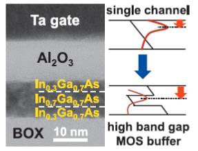
InGaAs MOS gate stack formation and the MOS interface control technologies, which are mandatory for realizing high performance InGaAs MOSFETs, are addressed with an emphasis on our recent achievements. Al2O3/InGaAs MOS gate stacks formed by Atomic Layer Deposition (ALD) are known as one of the most superior InGaAs MOS interfaces. The experimental results of Al2O3/InGaAs, HfO2/InGaAs and HfO2/Al2O3/InGaAs interfaces are presented. It is found that 1-nm-capaciatance equivalent thickness can be realized by HfO2/Al2O3/InGaAs gate stacks. Also, semiconductor inteface buffer layers inserted between InGaAs channels and gate oxides are shown to be effective in further improving the channel mobility.