抄録
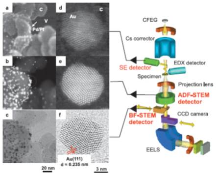
We innovated the secondary electron (SE) imaging technology with an aberration-corrected scanning transmission electron microscope (STEM). As a result, atomic resolution SE imaging has been achieved for the first time. We have successfully observed isolated single uranium atoms on carbon thin films using the SE signal. In addition, atomic-resolutionSE images were obtained not only from specimens containing heavy elements like uranium but also from those composed of light elements such as silicon and carbon. Because the SE signals are from the upper surface of specimen, imaging atomic lattice for thick specimens of 1 µm was demonstrated. This unique technology provides unprecedented application capabilities including 1) simultaneous atomic-resolution SE/STEM imaging to reveal topographical surface and bulk structure ; 2) simplified specimen preparation requirement for atomic-resolution electron microscopy ; and 3) imaging atomic structure for thicker than 1 µm specimens without having to use a million volt electron microscope.