特集: 光電子分光の新展開
電子デバイスのオペランド光電子分光実験
2016 年 37 巻 1 号 p. 25-30
詳細
2016 年 37 巻 1 号 p. 25-30
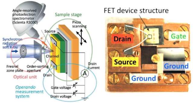
Scanning photoelectron microscopy (SPEM) is one of the most powerful tools for microfabricated electronic device analysis. In order to understand operation characteristics of real devices, “operando analysis”, i.e., measurement during device operation, is needed. In this report, we present our operando SPEM system, called “3D nano-ESCA” using synchrotron radiation soft X-ray. The 3D nano-ESCA enable us to perform nano-scale pin-point analysis and nondestructive depth profiling, thus we can investigate the effect of surfaces, interfaces and defects on transport characteristics. We have carried out the operando SPEM analysis of graphene field effect transistors (FETs) and organic FETs. Charge transfer region at a metal electrode/graphene channel was successfully detected for the first time. Moreover, pin-point photoemission spectroscopy on the channel under biasing at the gate and drain electrodes clarify energy alignment inside the devices.