Abstract
Metal oxide nano-microstructures are applied in photocatalytic surfaces, sensors
or biomedical engineering, proving the versatile utilization of nanotechnology.
However, more complex or interconnected nano-microstructures are still seldomly
met in practical applications, although they are of higher interest, due to
enhanced structural, electronic and piezoelectric properties, as well as several
complex biomedical effects, like antiviral characteristics. Here we attempt to
present an overview of the novel, facile and cost-efficient flame transport
synthesis (FTS) which allows controlled growth of different nano-microstructures
and their interconnected networks in a scalable process. Various morphologies of
nano-microstructures synthesized by FTS and its variants are demonstrated. These
nano-microstructures have shown potential applications in different fields and
the most relevant are reviewed here. Fabrication, growth mechanisms and
properties of such large and highly porous three-dimensional (3D) interconnected
networks of metal oxides (ZnO, SnO2, Fe2O3)
nano-microstructures including carbon based aerographite material using FTS
approaches are discussed along with their potential applications.
1. Introduction
Metal oxide nano-microstructures such as nanorods, nanowires, nanobelts,
nanotetrapods and others are being significantly investigated due to their new and
extraordinary properties appropriate for versatile nanotechnological
applications1–3). Fabrication of several
nanostructures from various metal oxides like ZnO, SnO2, TiO2,
and Fe2O3 has already been performed using several growth
techniques and their properties have been reported1–4). Among them, ZnO is one of the most investigated materials in the
last decades, because of its wide and direct bandgap of ∼3.37 eV, large
exciton binding energy ∼60 meV and simplicity in growth1–3, 5). Due to its hexagonal-wurtzite crystal structure, Zn and O
terminated polar surfaces, different growth rates of the diverse crystal planes,
quasi-1-Dimensional (Q1D) nanostructures and complex morphologies from ZnO can be
synthesized. The direct bandgap which lies in the near ultraviolet -(UV) spectral
region and alternating Zn and O stacking layers enable ZnO nanostructures to exhibit
exceptional optical, luminescent6, 7) and electrical
properties5, 8–11). Bendability is also a very important property
required for different applications but bulk ceramics or metal oxides are brittle in
nature1–3). However, their Q1D structures
can bend elastically to larger curvatures once their thickness is in the nanoscopic
range1–3, 12). Nanorods and nanowires from ZnO have already
shown interesting piezoelectric properties for energy or mechanical
applications1–3, 13). Illumination of ZnO nanostructures with UV
light creates electron-hole pairs and thus changes their conductivity and enables
its uses for photodetectors14–19).
Additionally ZnO nano-microstructures are extensively investigated for light
emitting diodes and gas sensing applications14, 20–22). By
doping with different elements it is possible to enhance the sensing performances of
ZnO nanostructures23, 24). ZnO nanostructures have also
been considered as biocompatible material and therefore have been significantly
employed in biomedical applications25–29).
Furthermore, the interconnected nanostructures can build up microstructures or even
highly porous 3D interconnected macroscopic networks which avoid risks of toxicity
as a result from nanoscale particles. However, several issues like actual effect and
cytotoxicity are still open25, 30). In general,
various physical and chemical properties of different metal oxide nanostructures
depend not only on their sizes and morphologies, but also on the synthesis
techniques and experimental conditions (or technological ‘history’).
Despite of such interesting applications, the scientific community is still looking
for appropriate synthesis techniques, which can facilitate the versatile fabrication
of different networked metal oxide nano-microstructures for practical applications
in a cost-effective and scalable process.
Several synthesis methods have been utilized for growing different metal oxide
nano-microstructures. Vapor-liquid-solid (VLS) mechanism31) has been a very common process for controlled
growth of ZnO nanostructures like nanorods32, 33), nanowires34), nanotrees35), and interpenetrating ZnO nanosails bridge36) at junctions, etc. Other
methods like hydrothermal synthesis37–39),
chemical vapor deposition (CVD)40), microwave chemistry41), combustion synthesis42), plasma process43, 44), electrochemical deposition14, 45, 46), gas phase synthesis47) and flame based synthesis48–51) have been employed to grow metal oxide
nanostructures, especially ZnO nanostructures. Thus, an easy scalable,
cost-effective and facile synthesis method which can produce large amounts of
different metal oxide nano-microstructures is still a highly demanded aspect for
various applications.
Although most of the mentioned synthesis methods enable controlled growth of metal
oxide nanostructures, but they lack with the feature of in-situ
integration of such nanostructures directly on the chip in form of device. One
requires nanoscale electrical contacts and this further hinders their application.
To overcome such technological limitations a thin film fracture approach52) was invented recently. It
allows direct fabrication of desired metal or metal oxide nanostructures between the
electrical contacts on the sensor or device chip53–55). However, most desirable technological procedures are based on
facile growth and direct integration of nanostructures on chip in a single step.
Fabrication of large and porous 3D networks from interconnected metal oxide
nanostructures might be an ideal choice for utilizing its nanoscale properties at
macroscopic scale for different industrial technologies. It is important to mention
that it has not been explored in details yet. Only few groups56, 57) have reported fabrication of 3D networks from
metal oxide nanostructures using different techniques.
Recently Adelung and co-workers58, 59) have
introduced a very simple and novel flame transport synthesis (FTS) approach which
allows facile fabrication of versatile metal oxide nano-microstructures and their
macroscopic networks. These FTS synthesized metal oxide nano-microstructures have
already shown promising applications in different directions60–66). ZnO nanoseaurchin and tetrapod type
structures grown by FTS approach exhibit strong potential of blocking the viral
(herpes simplex virus type-1 and type-2) entry into the cells60, 61). The submicron size tetrapods can be utilized
for advanced linking technologies64) and designing multifunctional composites, e.g., new concept of
self-reporting material65). In this context, FTS approach offers a simple way to fabricate
large size 3D networks from interconnected metal oxide nano-microstructures with
desired porosity and mechanical strength. These 3D networks are stable at high
temperatures (up to 〜1400°C), electrically conducting and therefore
can be used in advanced technological applications57). Recently, such 3D interconnected ZnO
tetrapods networks were used as templates for the guided growth of the carbon based
new aerographite material, which is currently one of the least dense materials in
the world67). In this
paper, we present the growth of different metal oxide nano-microstructures and their
interconnected 3D networks by FTS approach and its variants. Different morphologies,
growth mechanisms and properties of nanomaterials are presented and discussed in
detail.
2. Experimental
2.1 Materials Requirements
Flame transport synthesis (FTS) method and its variants59) mainly require microscale diameter
spherical metal particles as precursor materials, sacrificial polymer (e.g.,
polyvinyl butyral (PVB), etc.) and ethanol for mixing homogeneously in slurry
form. In our works59), different metal particles powders (Zn, Fe, Sn, Bi, Al, Si
etc.) with diameters in the range from 3 μm to 45 μm have been
used (purchased from GoodFellow UK, purities 99.9% to 99.99%).
PVB powder (supplied by Kuraray Europe GmbH, Germany) was used as sacrificial
polymer for the presented experiments. A simple muffle type furnace which can
rapidly heat up to high temperatures was used for our experiments. Also, in
these experiments, no gas control or vacuum equipment is necessary because it
works in normal air environment. Some ceramic plates, crucibles, and cylinders
and conventional burner type equipments are required for different variants of
FTS approach59).
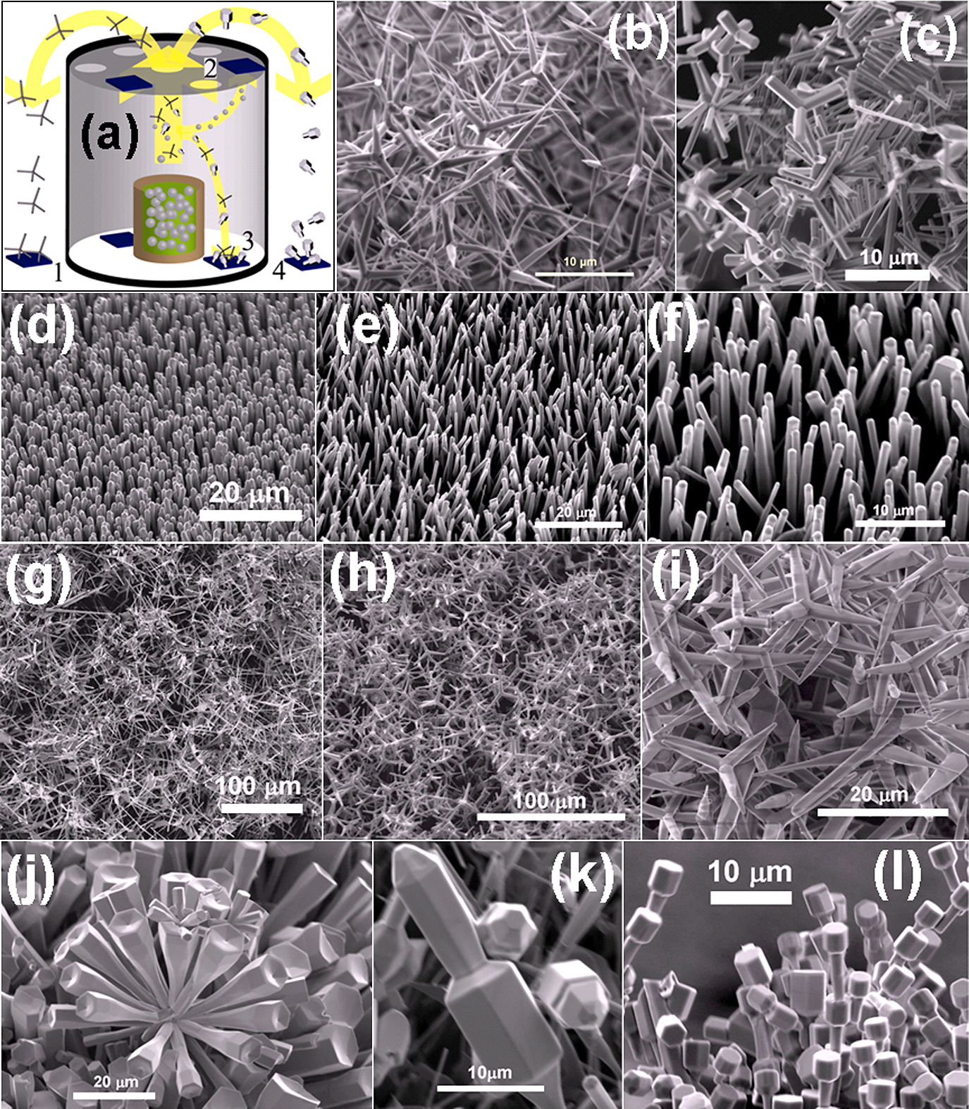
2.2 Flame transport approach and its variants
The first variant of FTS approach (Fig.
1a) enables the fabrication of nanoseaurchin type structures59). For this process the
slurry mixture of precursor metal -microparticles, PVB powder and ethanol is
prepared in appropriate ratio and coated on desired substrates (Si, Aluminum
etc.). After drying the coated layer on the substrate, it is heated at different
temperatures (depending upon the type of precursor metal microparticles) and
formation of nanoseaurchin type structures occurs. For example, to synthesize
ZnO nanoseaurchins, a temperature above 550°C is sufficient. According
to our experimental evidence for iron oxide nanoseaurchins, the optimum
temperature is about 900°C. By increasing the precursor metal particle
ratio versus PVB in the slurry and by increasing the thickness of the coated
layer, it was possible to fabricate a 3D network from nanoseaurchins (Fig. 2a) in a similar manner. The
second variant of FTS approach allows direct transformation of precursor metal
microparticles into metal oxide nano-microstructures in powder form (Fig. 3a–3d). The mixture Zn:PVB with ratio 1:2
was filled in the ceramic crucible and heated up to 900°C, which results
in formation of different ZnO nano-microstructures in form of powder. These
nano-microstructures can be harvested from the furnace and accordingly utilized
for desired applications59). The yield per experiment mainly depends on the several
factors like ratio of Zn to PVB, amount of Zn and PVB mixture and temperature of
the furnace etc. In each standard experiment for ZnO tetrapods production
(Zn:PVB = 1:2, 900°C, 30 minutes) the yield was around
30–40% and in each experiment and we harvest about 15–20
grams of ZnO tetrapods depending upon initial conditions. The third variant of
FTS approach utilizes an in-house ceramic cylinder arrangement (Fig. 5a) and it enables controlled
synthesis of different quasi-1D nano-microstructures and their networked
bridges. The fourth variant utilizes a simple burner approach (Fig. 6a) in which the precursor metal
microparticles are directly inserted into the oxygen and propane gas mixture
inside the burner tube. On their way in the flame, these precursor metal
microparticles are converted into various metal oxide nano-microstructures
within milliseconds and can be collected in form of powder or
in-situ integrated on the substrate/chip as per
requirements59).
The main aim of this paper is to provide an overview of different structures,
which can be synthesized using proposed FTS approaches for practical
applications. More technical details about ratios, growth conditions,
temperature time and substrate positions can be found in previous
works58, 59).
2.3 Characterizations:
The obtained nano-microstructures by FTS approach were characterized using
scanning electron microscope (20 keV Philips-FEI XL30 equipped with
LaB6 filament). Electromechanical measurements of Q1D, 2D and 3D
networks were performed by using a home made setup which includes a
micro-manipulator, a Keithley 2400 Sourcemeter, and a computer-controlled
laboratory balance with the help of a LabView program59).
3. Results and discussions
3.1 Growth of metal oxide nanoseaurchin structures using first variant of FTS
approach
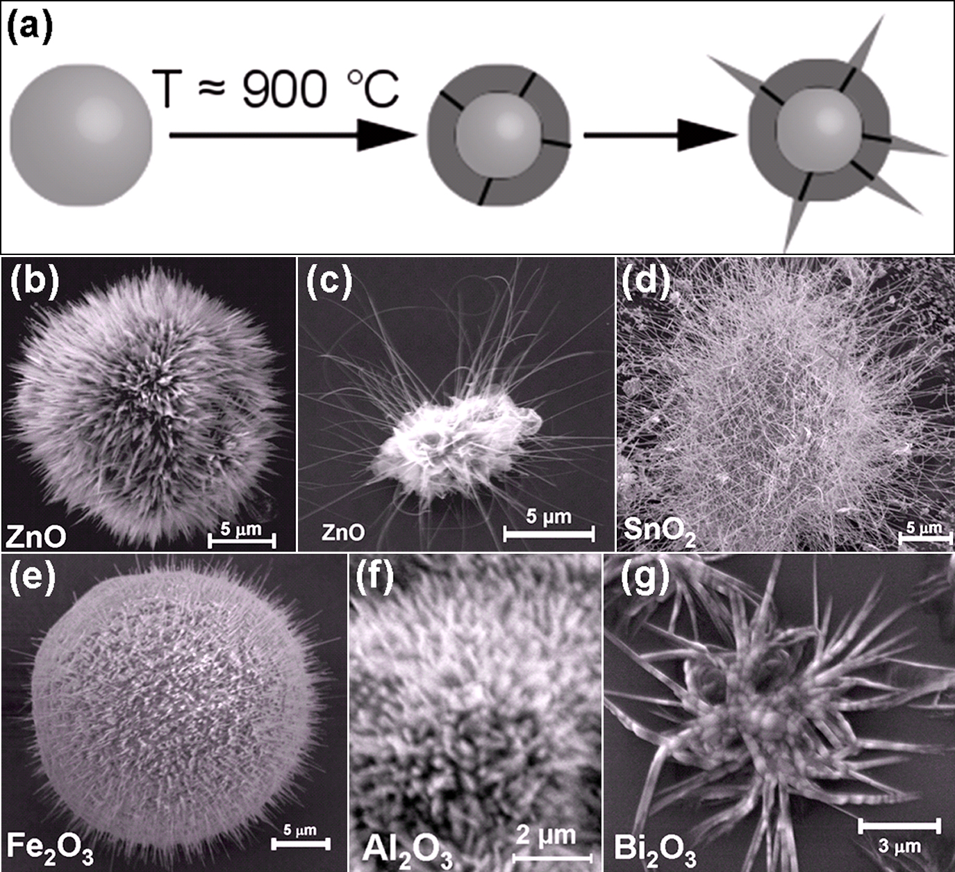
Fig. 1 demonstrates the growth
mechanism of nanoseaurchin type structure and few examples of already
synthesized nanoseaurchins from different metal oxides (ZnO, SnO2,
Fe2O3, Al2O3,
Bi2O5). To grow ZnO nanoseaurchins, a dilute slurry
mixtures from Zn, PVB and ethanol [Zn:
{PVB:Ethanol}=1:3{1:2}] was
prepared and coated on Si substrates. After drying the slurry coated substrate
was heated at 600°C in the muffle furnace for 2 hours. Depending upon
the requirements the ratios of Zn, PVB and ethanol were varied and the coated
substrates were heated above 600°C for different durations to synthesize
various types of seaurchins59). In similar manner, nanoseaurchins of several other metal
oxides have been successfully grown and can be found in previous work59).
For the growth of core-spike nanoseaurchins (Fig. 1), the crystalline quality of precursor metal
micro-particles as well as processing temperature play very important roles. The
sacrificial polymer (PVB) and ethanol mixture exhibit double roles: (i) it
maintain necessary separation between precursor microparticles which prohibits
the agglomeration of metal microparticles and (ii) during heating it provides
necessary local environmental control for nanospike growth on the surface of
microscopic core. Also above certain temperature (below the nanospike growth)
the PVB decomposes entirely and leaves no fingerprints behind in the grown
seaurchins or nanostructures, since it contain only C and O. The heating ramp
rate of the furnace is the most important parameter for growth of
nanoseaurchins, e.g., faster heating rates result in a better growth of such
micro-nanostructures (we used furnace with ramp rate above 100°C/min).
It has been observed that the metal oxide nanospikes were synthesized on the
surface of precursor metal microparticles only when the growth condition is far
from thermal equilibrium. Under such circumstances, the kinetic growth processes
dominate and it leads to a nanospike growth on the substrate/crucible surface.
This type of the spherical precursor microparticles exhibit surface defects,
like reconstructed surface and grain boundaries68). It seems that the grain boundaries most
likely offer the energetically favorable nucleation sites to initiate the
nanospike growth68). These nanospikes were investigated in details using
cross-sectional high resolution transmission electron microscopy along with
precession electron diffraction studies and it was observed that they consist of
twin boundary propagating along the c-axis69). Such ZnO nanoseaurchin
structures show their promising application as potential candidate for blocking
the viral (HSV-1) entry into the cells60). Further work on this kind of
micro-nanostructures is in progress.
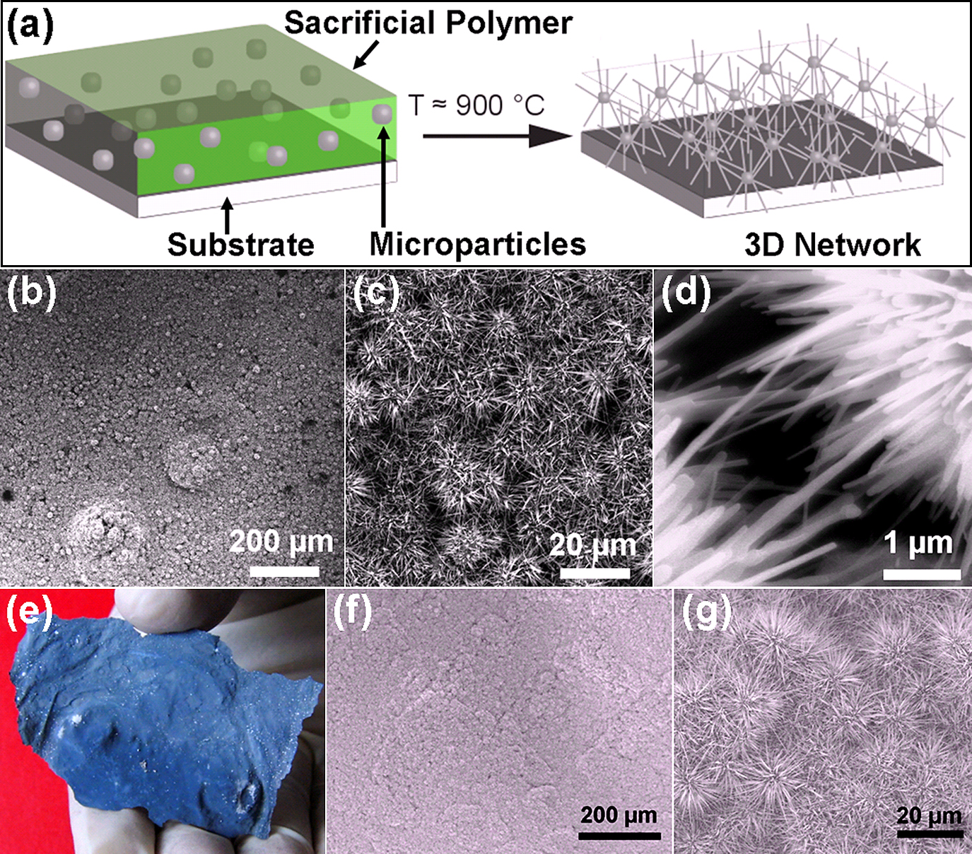
As mentioned already that growth of 3D interconnected network from metal oxide
nanostructures is a highly demanded aspect for practical applications. Using the
growth concept of nanoseaurchins, we have successfully grown large 3D
interconnected networks from core-spike nanoseaurchins. The schematic drawing
for 3D network growth is demonstrated in Fig. 2a in which a thick layer of slurry mixture is coated
on the substrate. The ratio of metal microparticles, PVB and ethanol is kept in
such a manner that the precursor metal particles are homogenously dispersed in
the slurry and during coating they are well separated by sacrificial polymer
layer (mixed with ethanol). After drying the substrate with slurry is heated
rapidly up to higher temperature (typically ∼600°C for ZnO, and
∼900°C for Fe2O3, SnO2,
Bi2O3 and Al2O3)59). Because of rapid heating
process, the growth of nanospikes on surface of precursor metal particles is
initiated like demonstrated in Fig.
1. The sacrificial polymer layer plays a crucial role here as it
maintains the necessary separation between microscopic particles and at the same
time nanospikes grow and form interconnecting bridges between individual
cores59). These
interconnecting nanospike bridges provide mechanical strength to the
network59). Using
this concept, large 3D interconnected networks from ZnO nanoseaurchins were
successfully grown and are shown by zoom-in series of SEM images in Fig. 2 (b–d) (from left to
right). The interconnecting nanospike bridges can be clearly seen in high
magnification SEM image in Fig.
2d.
A large 3D network from ZnO nanoseaurchins grown on Aluminum substrate (shown in
Fig. 2e) following a similar FTS
approach. Such kind of networks were investigated by SEM and confirmed that it
is entirely made from interconnecting core-spike nanoseaurchins, as presented in
Fig. 2(f). Its corresponding
higher magnification SEM image is shown in Fig. 2(g). The 3D networks from ZnO nanoseaurchins have
been successfully grown and optimized. However experiments for other metal oxide
3D networks are currently under progress.
The second variant of FTS approach enables direct conversion of precursor metal
microparticles into nanostructures within the flame created due to burning of
sacrificial polymer (PVB). The mixture of precursor metal microparticles and PVB
(1:2 ratio by weight) is filled in the ceramic crucible which is placed inside
the furnace and heated rapidly up to temperature of 900°C (for Zn
microparticles). Because of high heating rate the PVB starts burning and creates
intense flame59).
Then, the precursor metal microparticles travel in the flame stream and due to
of high flame temperature are converted in ZnO nano-microstructures. After
reaching 900°C, the temperature of the furnace is maintained constant
for different time spans (ranging from 30 minutes to 4 hours depending upon the
requirements) for proper growth of specific nano-microstructures. The role of
sacrificial polymer (PVB) is very important in FTS process, as it maintains the
separation of metal microspheres, creates the flame and also enables necessary
environmental conditions for nano-microstructures growth59).
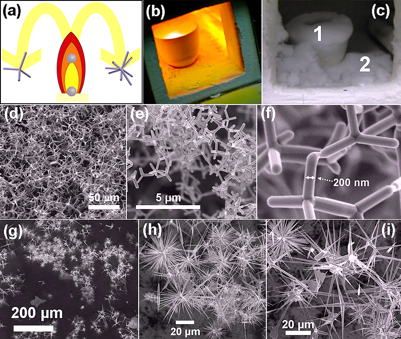
The conversion principle of precursor metal microparticles into the flame is
demonstrated in Fig. 3a. For
simplicity reasons only two types of structures (tetrapods and multipods) are
shown in the schematic however structures with various complex morphologies have
been grown. Fig. 3b shows the
digital camera image of the on going FTS process and the intense yellow flame in
the centre shows the turbulent stream of flame in which microparticles are being
converted into nano-microstructures. Once the process time is achieved, the
furnace was turned off. After cooling one can see the crucibles and the base of
the furnace are entirely covered with snowflake type white powder (Fig. 3c). These snowflake type powders
consist of tetrapods, multipodes, branched ZnO nano-microstructures depending
upon the location in the furnace. The snowflake type powder was harvested from
positions 1 and 2 (Fig. 3c) was
analyzed inside SEM. Morphological studies of the powder harvested from position
1 (Fig. 3c), i.e., from the
crucible, revealed that it mainly consists of ZnO tetrapod structures with
different sizes as shown by SEM images in Fig. 3(d–f) at increasing magnifications (from
left to right). However, the fluffy powder at the base (position 2, Fig. 3c) consists of ZnO tetrapods,
ZnO multipodes and several other complicated shapes as evident by SEM images in
Fig. 3(g–i) at
increasing magnifications (from left to right). The ZnO tetrapod and multipode
structures can be harvested and can be utilized accordingly for desired
applications. The ZnO tetrapods have shown promising applications, as antiviral
agents60, 61), in advanced linking
technology64) and
designing self-reporting composites65).
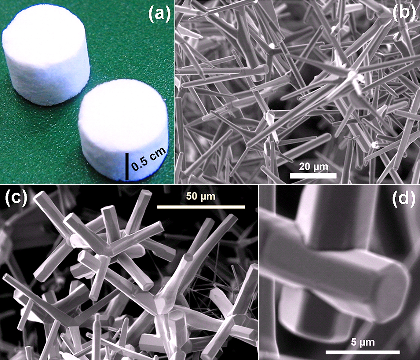
Since growth of desired 3D networks was the strong motivation for our research,
the harvested ZnO tetrapods from second variant of FTS were further processed to
synthesize different interconnected networks59). Appropriate amounts of tetrapods were
filled in open cylindrical ceramic scaffolds, pressed and reheated at high
temperature (∼1150°C) for 4 hours. Such a reheating results in
the formation of interconnections between tetrapod arms providing mechanical
strength to the entire network59). For example, the 3D ZnO networks fabricated using this
approach is shown in Fig. 4a.
These 3D networks were analyzed inside SEM in details to study the underlying
growth process. Fig.
4(b–d) shows the SEM images taken inside the network at different
magnifications. It is clearly visible that at some places the tetrapod arms
interpenetrate fully (Fig. 4d is
a high magnification of Fig. 4b)
and at some places they interpenetrate partially (Fig. 4c). It seems that formation of interconnections
initiates from the positions where the arms are touching each other during
re-heating. However, further investigations for understanding the exact
mechanism of arms’s interpenetrations are under progress59).
Based on proposed approach macroscopic and highly porous (up to 98%) 3D
interconnected networks were fabricated using ZnO tetrapods59). These networks are
electrically conducting and high temperatures stable (up to 1400°C).
Flexibility of 3D porous networks is a very important property which enables
their use for various applications. It was observed that by varying the density,
one can tune the elastic modulus of these networks from few kPa to rubber
elastic region (less than 100 MPa) and thus they fall in the category of
flexible ceramics59). These flexible conducting highly porous 3D interconnected
networks exhibit potential applications for new advanced technologies. Recently,
these 3D networks have been used as templates for guided growth of carbon based
aerographite material67).
The third variant of FTS offers controlled growth of different Q1D metal oxide
nano-microstructures employing the cylindrical arrangement as shown in Fig. 5(a). The precursor metal
microparticles, sacrificial polymer and ethanol mixture (in form of slurry) is
placed in the crucible and the substrates can be mounted at positions 1 to 4
(Fig. 5a) for different
nano-microstructures. The cylindrical arrangement is inserted into the furnace
and heated at high temperatures in air environment. The cylinder arrangement
enables further control on the nanostructure growth process and Q1D
nanostructures, like nanorods, nanowires, nanonails and their large arrays can
be grown in a controlled manner59). The conversion mechanism of precursor microparticles in the
flame is similar like mentioned in Fig.
3(a) but inclusion of ceramic cylinder adds extra features. At positions
1 and 4 (Fig. 5a), the
nanostructure growth process is almost similar to that demonstrated in Fig. 3.
Nano-microstructures grown at position 2 and 3 (Fig. 5a) are quite different, because position 3 is
located inside the cylinder at the base surrounding the crucible and position 2
on the top holes, where substrates are mounted vertically downwards. SEM studies
from structures deposited on position 1 (Fig. 5a) confirmed the growth of different types of ZnO
tetrapods, as shown in Fig. 5b
and Fig. 5c. Growth of different
Q1D nanorods and their arrays occurs on substrates mounted at position 2, (Fig. 5a). On substrates at position 3,
located inside the cylinder, more converted nano-microstructures are deposited
during growth process and therefore 3D networks are formed. These 3D networks
are quite different as compared to those obtained by reheating the tetrapods
(Fig. 4). Since growth and
interpenetration simultaneously occur at position 3, these 3D networks are much
stiffer and exhibit relatively higher elastic modulus59).
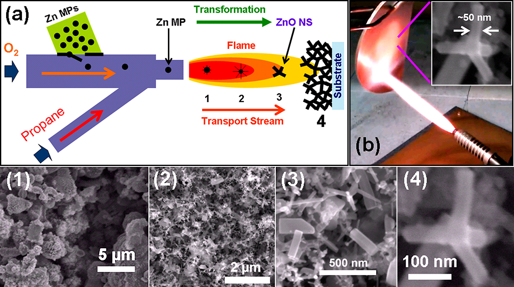
The fourth variant of FTS approach utilizes a burner equipped with Oxygen and
Propane gases for the flame as shown in Fig. 6a59).
The precursor Zn microparticles are inserted into the gas stream in controlled
manner and they travel along with the flame when coming out from the nozzle.
During their travel, these precursor metal microparticles are converted into
nano-microstructures because of very high flame temperature of the flame. These
nano-microstructures can be deposited on the substrates or collected in form of
powder depending upon the requirement.
The 3D interconnected networks can be synthesized if process is continued for
longer durations at same locations59). The conversion of Zn microparticles into
nano-microstructures depends on transport time within the flame and
transformation stages as marked by positions 1, 2 and 3 (Fig. 5a). A large copper plate coated
with ZnO tetrapods using burner approach is shown in Fig. 6b. The SEM images (1–3) presented in Fig. 6 correspond to particle
transformation stages shown in Fig.
6a. The image 4 in Fig. 6
shows SEM of a single ZnO nanotetrapod, which was coated on copper plate. More
details about different experiments are elaborated in previously published
paper59) and
experiments are still under progress to optimize the growth of other metal oxide
nano-microstructures. The FTS grown nano-microstructures have already shown
promising applications and few are summarized in the next section. Recently
using burner-FTS approach, an interconnected ZnO nanotetrapods network bridge
was directly integrated between electrodes in a chip for UV photodetector
applications which demonstrated very fast photodetection response70).
4. Applications of the ZnO networked structures
4.1 Antiviral activity of ZnO nanoseaurchins and tetrapods against HSV-1
The synthesized structures by FTS approach were tested for antiviral applications
and it was observed that ZnO nanoseaurchins and tetrapods (shown in Fig. 7a and 7b) block the HSV-1 viral entry into cells60). The confocal microscopy
images (A–C) in Fig. 7c
confirm the attachment of viruses on the surface of ZnO structures. The plot D
in Fig. 7c shows the HSV-1 entry
level into the cells in presence of unilluminated and illuminated ZnO structures
with UV light. It was observed that in presence of such ZnO structures, the HSV
viral entry level goes down as some viruses get attached on the ZnO surface.
After UV illumination of these ZnO structures, the HSV-1 viral entry into the
cells is significantly decreased because of enhanced attachment of viruses on
the ZnO surface60).

The HSV-1 entry mechanism into the cells is demonstrated by schematic drawing
shown in Fig. 7d. The HSV-1
virus exhibits heparan sulfate (HS) groups as virion envelop which interacts
with gD-receptors on the cells and enter into the cells. The presence of ZnO
nano-microstructures screens the HSV-1 entry into the cells as some viruses are
attracted by the oxygen deficient surfaces of ZnO nano-microstructures. After
preparation, the ZnO nano-microstructures are several times under sun-shine, it
is sufficient to create oxygen vacancies60). After UV illumination, further O
vacancies are created in such ZnO structures which enhance the virus attachments
on the ZnO surface and results in the significantly decreased HSV-1viral entry
into the cells decreased. More details can be found in previous work60).
4.2 Antiviral activity of nano-micro ZnO tetrapods against HSV-2
Since herpes simplex virus type 2 (HSV-2) is more fatal as compared to HSV-1 and
antiviral community is still waiting for appropriate treatments. We utilized the
ZnO tetrapods to study the HSV-2 viral entry into the cells61) and its antiviral activity
is demonstrated in Fig. 8. The
SEM images of ZnO tetrapods used for experiments with HSV-2 are shown in Fig. 8(a–c) at increasing
magnifications (from top to bottom). The confocal microscopy results of ZnO
tetrapods without and with HSV-2 viruses are shown in Fig. 8(d) and Fig. 8(e, f), respectively.
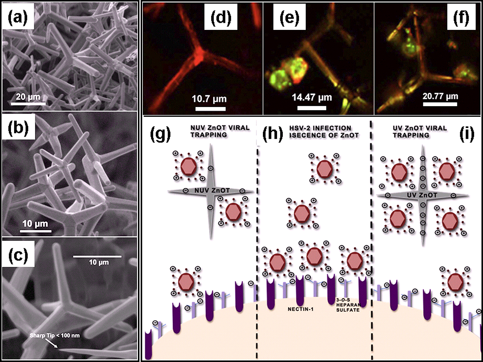
The HSV-2 viruses were labeled with green markers using a dye. The viral entry
mechanism of HSV-2 viruses into the cells in presence of ZnO tetrapods is
demonstrated in Fig.
8(g–i). As mentioned above, in presence of ZnO tetrapods, some
viruses are attached at the surface of ZnO tetrapod arms due to inherent oxygen
vacancies (Fig. 8g). In absence
of ZnO tetrapods, the HSV-2 viruses make normal entry into the cells in natural
manner (Fig. 8h). After UV
illumination on such ZnO tetrapods, the HSV-2 viral entry into the cells goes
significantly down (Fig. 8i)
because more viruses are attached on the surface of ZnO tetrapods arms due to
additional oxygen vacancies created by UV illumination61). Few studies relating to blocking
capability of these ZnO tetrapods have already reported in recently published
articles60, 61, 63). Further in-vivo experiments are under
progress to understand the process in more details. Similar phenomenon was
observed in case of SnO2 nanowire networks, synthesized by FTS
approach shows strong potential of blocking the HSV-1 entry into the
cells62). For
biomedical applications of different nano-microstructures, cytotoxicity is very
important issue and these nano-micro scale ZnO tetrapods exhibit very low level
of cytotoxicity as compared to conventional spherical nanoparticles and
ZnCl2 reference71), which implies towards better utilization in biomedical
engineering.
4.3 ZnO nano-micro tetrapods for advanced linking technology
A brand new method of joining polymers with low surface energy was developed by
the utilization of the ZnO nano-micro tetrapods (Fig. 9) produced by the second FTS variant shown
before59). This
method employs the convex shape of tetrapodal microparticles which works as an
anchor to mechanically interlock two polymer layers together. Its efficiency was
demonstrated by joining two extremely difficult-to-join polymer layers, namely
the poly(tetrafluorethylene) (PTFE) and cross-linked poly(dimethylsiloxane)
(PDMS)64). Both
polymers have very low surface energies and it was difficult to find a single
report describing that both polymers can be strongly joined by any technique.
Even PTFE alone is notoriously difficult to modify. The surface modification
methods developed before, such as plasma treatment and ion beam treatment,
require specific instruments. Chemical treatments are difficult and involve
hazardous chemicals with PTFE, which is highly chemically inert. The new method
achieved a peeling strength of 220 N/m by an easy applicable approach, without
modification of the chemical composition of each polymer layers64).
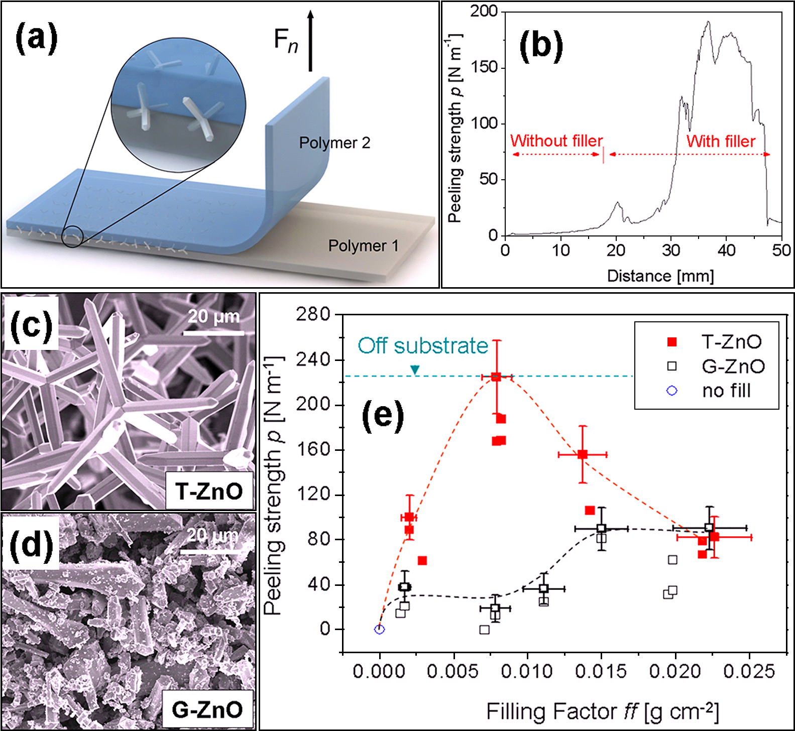
Fig. 9a demonstrates the adhesion
technology between two polymer layers employing ZnO tetrapods (T-ZnO) at the
interface between two layers. It was observed that with the T-ZnO at the
interface the peeking strength was improved significantly (Fig. 9b). In order to compare the
effect of shape, some ZnO tetrapods (Fig. 9c) were ground (G-ZnO), which resulted in microrod type structures
(Fig. 9d). These G-ZnO (ground
ZnO tetrapods) structures were also embedded at the interface between two
polymer layers and peeling strengths from both (T-ZnO and G-ZnO) were compared
which are shown in Fig. 9e. It
can be clearly seen that employing T-ZnO gives much better adhesion as compared
to G-ZnO. Since there was no chemical treatment applied to ZnO structures and
polymer surfaces, the strong adhesion is purely due to mechanical interlocking.
Therefore the concave shaped particles such as tetrapods produced by FTS
approach has shown unique potential in improving the mechanical adhesion of
polymer laminates64). More details can be found in report by Jin et al.64)
4.4 ZnO nano-micro tetrapods as fillers for fabricating self-reporting
composites
Semiconducting tetrapod type structures have already shown interesting stress
dependent luminescent responses72, 73). An
important possible application of tetrapodal shaped ZnO nano-microstructures in
polymers is the development of a new concept for self-reporting
materials65). The
concept assumed that, the deformation of the crystals induces changes in the
photoluminescence (PL) signal of the ZnO nano-microtetrapods and therefore it
can be used to indicate the stress state of the material. This concept was
tested by embedding the tetrapodal particles in an elastomeric matrix as shown
in Fig. 10a. Typical SEM image
of ZnO tetrapods used in the experiments are shown in Fig. 10b and digital camera image of the final prepared
T-ZnO: PDMS (Polydimethylsiloxane) composite is shown as inset in Fig 10b. Desired size and shape of
composite can be fabricated as reported by Jin et al.65) The PL spectra of T-ZnO: PDMS composites
with respect to tensile stress are shown in Fig. 10c. It can be seen that the intensity of blue PL
peak (from UV excitons in ZnO) remains constant but intensity of green PL peak
(∼523 nm) has increased which most likely appears from surface defects
in ZnO10, 11).
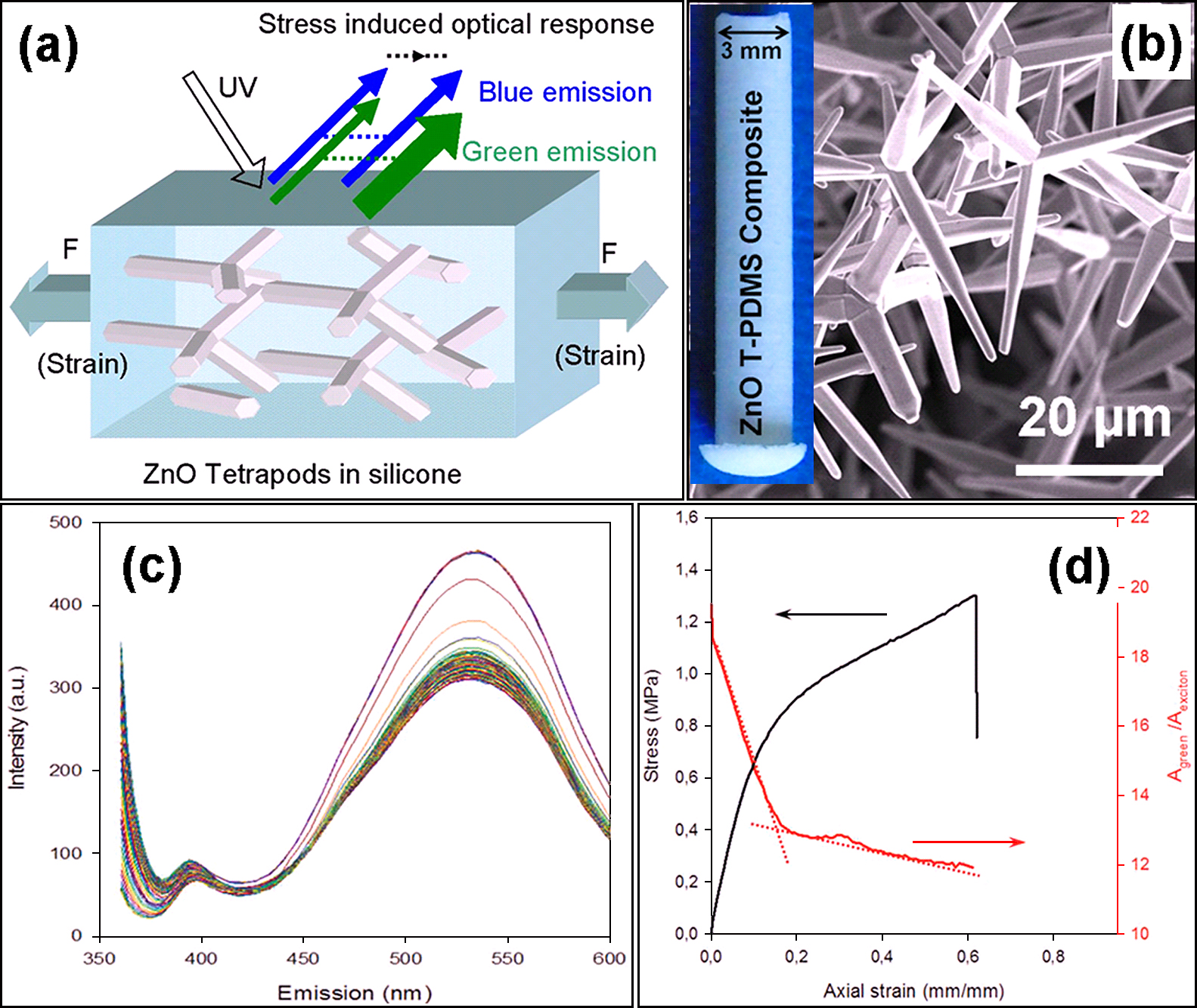
A strong correlation between the tensile stress and green PL signal was observed
as shown in Fig. 10d.
Furthermore, the polymer was reinforced by the addition of tetrapodal
microparticles, which was not the case in other stress-sensing mechanisms
involving photoluminescent particles as fillers65). Detailed analysis revealed that the
formation of network of tetrapodal micro-particles is important for such
correlations and a detailed monitoring of intensity ratio one might be able to
extract to damage informations inside the composites. Further details can be
found in the article by Jin et al.65)
4.5 ZnO 3D networks as templates for growth of ultra light weight aerographite
material
The 3D interconnected metal oxide nano-microstructures networks are extremely
important for practical applications. Next, we demonstrate an example of growing
new carbon based Aerographite material (shown in Fig. 11), which is one of lightest solid materials so
far67). The
interconnected networks from ZnO tetrapods were used as templates inside CVD
chamber for growth of aerographite material. It was observed that the material
growth follows exactly the tetrapods morphology and the existing
interconnections in the 3D ZnO network template. The hydrogen gas flowing in the
CVD chamber plays main role in the transformation of ZnO into aerographite as it
etches ZnO from the surface of ZnO tetrapods and simultaneously deposits carbon
at this place67).
It was reported that belt like early stage growth is most likely responsible for
this type of transformation of ZnO tetrapods into aerographite
material67). This
is an ultralight weight material with lot of interesting physical and chemical
properties suitable for different applications67). Just for demonstration, SEM images from
the fabricated aerographite material and some of its properties are summarized
in Fig. 11.
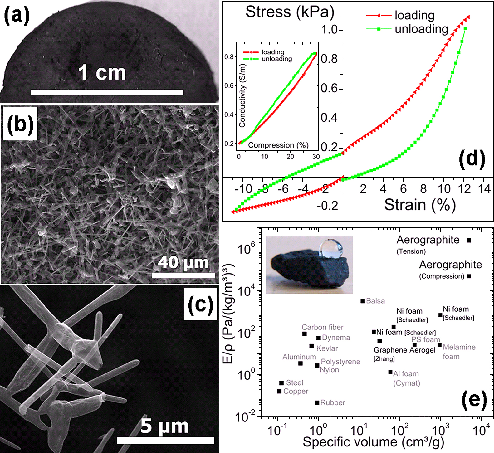
The 3D aerographite networks with desired sizes can be grown by proposed
technique. For example digital camera image of a large cylindrical (1.4 cm
diameter large with 1 cm height) aerographite network is shown in Fig. 11a and corresponding low and
high magnification SEM images are shown Fig. 11b and Fig. 11c respectively. The high magnification SEM image (Fig. 11c) confirms the hierarchical
hollow framework networks of microtubes inside aerographite network. Fig. 11e and d display mechanical data of
aerographite material. In Fig.
11d, a mechanical load cycle containing compressive and tensile load is
shown. The inset in Fig. 11d
shows how the electrical conductivity increases during the mechanical
compression in a similar experiment. Fig. 11e is an Ashby material selection map74) as it is a convenient guideline in modern
lightweight engineering. It compares the specific modulus and density for a
plenty of materials (including aerographite) because these two properties are
very crucial to build stiff and light parts from an individual material. The
here demonstrated Aerographite material exhibits interesting electromechanical
properties (Fig. 11d) and
material selection map (shown in Fig.
11e) suggests it to be a potential candidate for material engineering
applications67). It
is among one of the extremely porous materials (porosity >
99.9%) and still superhydrophobic in nature67). The aerographite material possesses a lot
of other interesting features suitable for various advanced applications and
more details can be found from the previous paper by Mecklenburg et
al.67)
5. Conclusion
In conclusion, we point out that proposed flame transport synthesis FTS and its
approaches offer really facile, cost-effective and scalable synthesis processes for
versatile micro-nanostructures of various metal oxides. It also enables successful
fabrication of different 3D interconnected networks with desired sizes, porosities,
electrical conductivities etc. The tunable elastic modulus of these 3D networks in
the range of rubber elastic region enables them as flexible ceramics for various
technological applications. Three-dimensional interpenetrated micro-nanostructures
can be used as appropriate networks for controlled growth different other structures
for example and ultralight weight aerographite material. The nano-micro-scale ZnO
tetrapods have already proved their promising applications in the direction of
biomedical engineering, advance linking technologies and designing self-reporting
composites etc. The controlled variant of FTS technology offers facile growth of
quasi-1D nanostructures and their arrays. Preliminary experiments using ultralong
single crystalline ZnO needles have shown promising features for applications in
various fields. Most relevant applications of the metal oxide micro-nanostructures
grown by FTS approach and its variants have been summarized in this paper and
several others are under progress.
Acknowledgements
YKM sincerely thanks to Prof. Sotiris E. Pratsinis (Particle Technology Laboratory,
ETH-Zurich) for kind invitation to write the article and to Ms. Natalie Winzer
(HOSOKAWA ALPINE Aktiengesellschaft, Germany) for her enormous patience in terms of
deadline extensions and reviewing. This project was funded by German Research
Foundation (DFG) under the schemes SFB 855-A5 and partially by SFB 677-C10 and
Ad/183/10-1. YKM and OL acknowledge the researcher fellowships from Alexander von
Humboldt Foundation at the University of Kiel, Institute of Materials Science,
Germany.
Author’s short biography
Yogendra Kumar Mishra

Yogendra Kumar Mishra is currently working as a senior research assistant and
habilitant in the Functional Nanomaterials Group at the Institute for Materials
Science in the University of Kiel, Germany. He received his Ph.D. in physics
(plasmonics) from Jawaharlal Nehru University, New Delhi, in September 2008, and
since October 2008 has been working in the Functional Nanomaterials Group. During
February 2009 to February 2011, he worked as an Alexander von Humboldt fellow in the
group. At Kiel, he introduced a new fabrication technique called ‘Flame
Transport Synthesis’ which allows the versatile fabrication of different
metal oxide nano-microstructures and their interconnected 3D networks.
Sören Kaps

Sören Kaps studied materials science at the University of Kiel and received
his diploma in 2008. He joined the group of Prof. Rainer Adelung (Functional
Nanomaterials) as a Ph.D. candidate in 2008. His research is focused on the
application of ZnO in magneto-electric sensors as in the DFG project SFB 855
Biomagnetic Sensing.
Arnim Schuchardt

Arnim Schuchardt received his B.Sc. (materials science) in 2008 at the University of
Kiel. In 2010 he received his M.Sc. (materials science) at the University of Kiel.
Since 2010, he has been a Ph.D. student in the Functional Nanomaterials Group,
Institute for Materials Science in the University of Kiel, Germany. He is mainly
working on the fabrication and electromechanical characterization of highly porous
carbon-based 3D networks (aerographite).
Ingo Paulowicz

Ingo Paulowicz is currently working as a Ph.D. candidate in the Functional
Nanomaterials Group at the Institute of Materials Science, University of Kiel,
Germany. He finished his M.Sc. in 2010 at the very same place on the synthesis and
characterization of tin oxide nanostructures. He prepared his B.Sc. at Hochschule
Bonn-Rhein-Sieg on the topic of laser-sintered titanium dioxide, which he finished
in 2008. His present field of work is mainly the synthesis of zinc oxide, in
particular via a modified burner approach synthesis (m-BAS).
Xin Jin

Xin Jin studied Physics at the East China Normal University in Shanghai. She obtained
her Master’s degree (2010) in material science and engineering from the
University of Kiel. Since 2010 she has been a Ph.D. candidate in the group of Prof.
Dr. Rainer Adelung (Functional Nanomaterials), University of Kiel, Kiel, Germany.
She is working mainly on the DFG project SFB677 which focuses on photoswitchable
adhesives. She recently introduced the new concept of joining the un-joinable
polymers employing ZnO tetrapods as linkers.
Dawit Gedamu

Dawit Gedamu is a Ph. D. candidate. in materials science at the Functional
Nanomaterials Group, Institute for Materials Science, University of Kiel. His
research interest mainly includes the synthesis of different metal and metal oxide
nanowires and their potential for various nanoelectronic devices and sensors. He
received an M.Sc. in material science and engineering in 2008 from the University of
Kiel, Kiel, Germany.
Sebastian Wille

Sebastian Wille is currently working as a leader of the dental materials group in the
Department of Prosthodontic, Propaedeutics and Dental Materials at the UKSH in Kiel
on various projects about dental materials. A key topic is the aging of dental
zirconia ceramics. He received a Ph.D. degree in materials science (Dr.-Ing.) from
the University of Kiel in May 2009. He continued working in the group of Functional
Nanomaterials in Kiel until December 2012 as a scientist, concentrating mainly on
several projects about the application and synthesis of metal oxide micro- and
nanostructures.
Oleg Lupan

Oleg Lupan is a research fellow supported by the Alexander von Humboldt Foundation at
the University of Kiel, Institute of Materials Science, Functional Nanomaterials. He
received his M.S. in microelectronics from the Technical University of Moldova (TUM)
in 1993. He received his Ph.D. in solid-state electronics, microelectronics and
nanoelectronics from the Institute of Applied Physics, Academy of Sciences of
Moldova in 2005. His post-doctorate research activities were carried out at the
CNRS, Paris, France, and the University of Central Florida, USA. He received his
doctor habilitate degree in 2011. He is an associate professor at the TUM. His
current research interests include nanosensors and optoelectronic devices.
Rainer Adelung

Rainer Adelung is a full professor and chairholder of the Functional Nanomaterials
Group established in 2007 at the Institute for Materials Science, University of
Kiel, Germany. He received his Ph.D. (rer. net) in physics in 2000 from the
Institute of Experimental and Applied Physics, University of Kiel, and during
2001–2002, he was at Case Western Reserve University in Cleveland (USA) as a
Feodor Lynen (Alexander von Humboldt) Research Fellow. In 2006 he finished
habilitation at the Institute for Materials Science in Kiel and then continued as a
Heisenberg Professor (DFG grant) with his own Functional Nanomaterials Group until
2012.
References
- 1) Wang, Z.
L. (2009):
ZnO nanowire and nanobelt platform for
nanotechnology, Mat. Sci. & Eng. R,
Vol. 64, pp.
33–71.
- 2) Wang, Z.
L. (2012):
From nanogenerators to piezotronics-A decade-long study of ZnO
nanostructures, MRS Bulletin, Vol.
37, pp.
814–827.
- 3) Zhou,
W. and
Wang, Z.
L. (2011):
“Three dimensional nano-architectures: Designing next generation
devices”, Springer
Publications, 233 Spring, New York, NY 10013,
US, ISBN 978-1-4419-9821-7.
- 4) Devan,
R. S.,
Patil, R.
A., Lin,
J. H. and
Ma, Y.
R. (2012):
One dimensional metal-oxide nanostructures: Recent developments
in synthesis, characterization, and applications, Adv.
Funct. Mater., Vol. 22, pp.
3326–3370.
- 5) Özgur,
U.,
Alivov,
Y.,
Liu,
C.,
Take,
A.,
Reshchhikov, M.
A., Dogan,
S.,
Avrutin,
V.,
Cho, J.
S. and Morkoc,
H. (2005):
A comprehensive review of ZnO materials and
devices, J. Appl. Phys., Vol.
98, pp. 41301.
- 6) Zeng,
H.,
Duan,
G., Li,
Y.,
Yang,
S. and
Cai,
W. (2010):
Blue luminescence of ZnO nanoparticles based on non-equilibrium
processes: Defect origins and emission controls, Adv.
Funct. Mater., Vol. 20, pp.
561–572.
- 7) Aubert,
T.,
Nerambourg,
N.,
Saito,
N.,
Haneda,
H.,
Ohashi,
N.,
Mortier,
M.,
Cordier,
S. and
Grasset,
F. (2013):
Tunable visible emission of luminescent hybrid nanoparticles
incorporating two complementary luminophores: ZnO nanocrystals and
[Mo6Br14]2− nanosized
cluster units, Part. Part. Syst. Charact., Vol.
30, pp.
90–95.
- 8) Lupan,
O.,
Pauporte,
T. and
Viana,
B. (2010):
Low-voltage UV-electroluminescence from ZnO-nanowire array/p-GaN
light-emitting diodes. Adv. Mater., Vol.
22, pp.
3298–3302.
- 9) Lupan,
O.,
Chai,
G.,
Chow,
L.,
Emelchenko, G.
A., Heinrich,
H.,
Ursaki, V.
V., Gruzintsev,
A. N. and
Redkin, A.
N. (2010):
Ultraviolet photoconductive sensor based on single ZnO
nanowire, Phys. Status Solidi A, Vol.
207, pp.
1735–1740.
- 10) Lupan,
O.,
Pauporté,
T.,
Ursaki, V.
V. and Tiginyanu,
I. M.
(2011): Highly luminescent columnar ZnO films grown
directly on n-Si and p-Si substrates by low-temperature electrochemical
deposition, Opt. Mater., Vol.
33, pp.
914–919.
- 11) Lupan,
O.,
Pauporté,
T.,
Tiginyanu, I.
M., Ursaki,
V. V.,
Heinrich,
H. and
Chow,
L. (2011):
Optical properties of ZnO nanowire arrays electrodeposited on n-
and p-type Si (1 1 1): Effects of thermal annealing,
Mater. Sci. Eng. B, Vol. 176, pp.
1277–1284.
- 12) Hoffmann,
S.,
Utke,
I.,
Moser,
B.,
Michler,
J.,
Christiansen, S.
H., Schmidt,
V.,
Senz,
S.,
Werner,
P.,
Gösele,
U. and
Ballif,
C. (2006):
Measurement of the bending strength of
vapor–liquid–solid grown Silicon nanowires,
Nano Lett., Vol. 6, pp.
622–625.
- 13) Desai,
A. V. and
Haque, M.
A. (2007):
Mechanical properties of ZnO nanowires,
Sensor and Actuat. A-Phys., Vol.134, pp.
169–176.
- 14) Zhai, T.
Y., Fang,
X. S.,
Liao, M.
Y., Xu,
X. J.,
Zeng, H.
B., Bando,
Y. and
Golberg,
D. (2009):
A comprehensive review of one-dimensional metal-oxide
nanostructure photodetectors, Sensors Vol.
9, pp.
6504–6529.
- 15) Fang, X.
S., Bando,
Y.,
Gautam, U.
K., Zhai,
T. Y.,
Zeng, H.
B., Xu,
X. J.,
Liao, M.
Y. and Golberg,
D. (2009):
ZnO and ZnS nanostructures: Ultraviolet-light emitters, lasers,
and sensors, Critical Rev. Solid State & Mat.
Sci., Vol. 34, pp.
190–223.
- 16) Lupan,
O.,
Pauporté,
T.,
Bahers, T.
L., Viana,
B. and
Ciofini,
I. (2011):
Wavelength-emission tuning of ZnO nanowire-based light-emitting
diodes by Cu doping: Experimental and computational insights,
Adv. Funct. Mater., Vol. 21, pp.
3564–3572.
- 17) Chai, G.
Y., Chow,
L.,
Lupan,
O.,
Rusu,
E.,
Stratan, G.
I., Heinrich,
H.,
Ursaki, V.
V. and Tiginyanu,
I. M.
(2011): Fabrication and characterization of an
individual ZnO microwire-based UV photodetector, Solid
State Sci., Vol. 13, pp.
1205–1210.
- 18) Hu,
L.,
Yan,
J.,
Liao,
M.,
Xiang,
H.,
Gong,
X.,
Zhang,
L. and
Fang,
X.
(2012):An optimized ultraviolet-A light
photodetector with wide-range photoresponse based on ZnS/ZnO biaxial
nanobelt, Adv. Mater., Vol.
24, pp.
2305–2309.
- 19) Chow,
L.,
Lupan,
O.,
Chai, G.
Y. (2010):
FIB fabrication of ZnO nanotetrapod and
cross-sensor, Phys. Status Solidi-B., Vol.
247, pp.
1628–1632.
- 20) Lupan,
O.,
Pauporté,
T.,
Bahers, T.
L., Ciofini,
I. and
Viana,
B. (2011):
High Aspect Ratio Ternary Zn1-xCdxO
Nanowires by Electrodeposition for Light-Emitting Diode
Applications, J. Phys. Chem. C., Vol.
115, pp.
14548–14558.
- 21) Lupan,
O.,
Ursaki,
V.V.,
Chai,
G.,
Chow,
L.,
Emelchenko, G.
A., Tiginyanu,
I. M.,
Gruzintsev, A.
N. and Redkin,
A. N.
(2010): Selective hydrogen gas nanosensor using
individual ZnO nanowire with fast response at room temperature,
Sensor and Actuat. B-Chem., Vol. 144, pp.
56–66.
- 22) Lupan,
O.,
Chow,
L.,
Pauporté,
T.,
Ono, L.
K., Cuenya,
B. R. and
Chai,
G. (2012):
Highly sensitive and selective hydrogen single-nanowire
nanosensor, Sensor and Actuat. B-Chem., Vol.
173, pp.
772–780.
- 23) Shishiyanu,
S. T.,
Lupan,
O.,
Monaico, E.
V., Ursaki,
V. V.,
Shishiyanu, T.
S. and Tiginyanu,
I. M.
(2005): Photoluminescence of chemical bath deposited
ZnO:Al films treated by rapid thermal annealing, Thin
Solid Films, Vol. 488, pp.
15–19.
- 24) Chow,
L.,
Lupan,
O.,
Chai,
G.,
Khallaf,
H.,
Ono, L.
K., Cuenya,
B. R.,
Tiginyanu, I.
M., Ursaki,
V. V.,
Sontea,
V. and
Schulte,
A. (2013):
Synthesis and characterization of Cu-doped ZnO one-dimensional
structures for miniaturized sensor applications with faster
response, Sensor and Actuat. A, Vol.
189, pp.
399–408.
- 25) Wahab,
R.,
Kaushik, N.
K., Verma,
A. K.,
Mishra,
A.,
Hwang, I.
H., Yang,
Y. B.,
Shin, H.
S. and Kim,
Y. S.
(2011): Fabrication and growth mechanism of ZnO
nanostructures and their cytotoxic effect on human brain tumor U87, cervical
cancer HeLa, and normal HEK cells, J. Biol. Inorg.
Chem., Vol. 16, pp.
431–442.
- 26) Gunawan,
C.,
Teoh, W.
Y.,
Ricardo,
Marquis, C.
P. and Amal,
R. (2013):
Zinc oxide nanoparticles induce cell filamentation in E.
coli, Part. Part. Syst. Charact., Vol.
30, pp.
375–380.
- 27) Wahab,
R.,
Dwivedi,
S.,
Umar,
A.,
Singh,
S.,
Hwang,
I.,
Shin, H.
S., Musarrat,
J.,
Al-Khedhairy, A.
A., Kim,
Y. S.
(2013): ZnO nanoparticles induce oxidative stress in
Cloudman S91 melanoma cancer cells. J. Biomed.
Nanotechnol., Vol. 9, pp.
441–449.
- 28) Wahab,
R.,
Kaushik, N.
K., Kaushik,
N.,
Choi,
E.H.,
Umar,
A.,
Dwivedi,
S.,
Musarrat,
J. and
Al-Khedhairy, A.
A. (2013):
ZnO nanoparticles induces cell death in malignant human T98G
gliomas, KB and non-malignant HEK cells, J. Biomed.
Nanotechnol., Vol. 9, pp.
1181–1189.
- 29) Umar,
A.,
Chauhan,
M.,
Chauhan,
S.,
Kumar,
R.,
Sharma,
P.,
Tomar, K.
J., Wahab,
R.,
Al-Hajry,
A. and
Singh,
D. (2013):
Applications of ZnO nanoflowers as antimicrobial agents for
Escherichia-Coli and enzyme-free glucose sensor, J.
Biomed. Nanotechnol., Vol. 9, pp.
1794–1802.
- 30) Nie,
L.,
Gao,
L.,
Feng,
P.,
Zhang,
J., Fu,
X.,
Liu,
Y.,
Yan, X.
and Wang,
T. (2006):
Three-dimensional functionalized tetrapod like ZnO nanostructures
for plasmid DNA delivery, Small, Vol.
2, pp.
621–625.
- 31) Wagner,
R. S. and
Ellis, W.
C. (1964):
Vapor liquid solid mechanism of single crystal
growth, Appl. Phys. Lett., Vol.
4, pp. 89.
- 32) Mishra,
Y. K.,
Mohapatra,
S.,
Singhal,
R.,
Avasthi, D.
K., Agarwal,
D. C. and
Ogale, S.
B. (2008):
Au-ZnO: A tunable localized surface plasmonic
nanocomposite, Appl. Phys. Lett., Vol.
92, pp. 43107.
- 33) Mishra,
Y. K.,
Chakravadhanula, V. S.
K., Hrkac,
V.,
Jebril,
S.,
Agarwal, D.
C., Mohapatra,
S.,
Avasthi, D.
K., Kienle,
L. and
Adelung,
R. (2012):
Crystal growth behaviour in Au-ZnO nanocomposite under different
annealing environments and photoswitchability, J. Appl.
Phys., Vol. 112, pp.
064308.
- 34) Yang,
P.,
Yan,
H.,
Mao,
S.,
Russo,
R.,
Yan,
H.,
Saykally,
R.,
Morris,
N.,
Pham,
J., He,
R. and
Choi, H.
J. (2012):
Controlled growth of ZnO nanowires and their optical
properties, Adv. Fun. Mater., Vol.
12, pp.
323–331.
- 35) Dick, K.
A., Deppert,
K.,
Larsson, M.
W., Martensson,
T.,
Seifert,
W.,
Wallenberg, L.
R. and Samuelson,
L. (2004):
Synthesis of branched ‘nanotrees’ by controlled
seeding of multiple branching events, Nat.
Mater., Vol. 3, pp.
380–384.
- 36) Jebril,
S.,
Kuhlmann,
H.,
Müller,
S.,
Ronning,
C.,
Kienle,
L.,
Duppel,
V.,
Mishra, Y.
K. and Adelung,
R. (2010):
Epitactically interpenetrated high quality ZnO nanostructured
junctions on microchips grown by the vapor-liquid-solid method,
Cryst. Growth Des., Vol. 10, pp.
2842–2846.
- 37) Lupan,
O.,
Chow,
L.,
Chai,
G. and
Heinrich,
H. (2008):
Fabrication and characterization of Zn-ZnO core-shell
microspheres from nanorods, Chem. Phys. Lett.,
Vol. 465, pp.
249–253.
- 38) Chow,
L.,
Lupan,
O.,
Heinrich,
H. and
Chai,
G. (2009):
Self-assembly of densely packed and aligned bilayer ZnO nanorod
arrays, Appl. Phys. Lett., Vol.
94, pp. 163105.
- 39) Peng,
Y.,
Huo,
D.,
Zheng,
L. and
Qian,
Z. (2012):
A simple hydrothermal method for the growth of ZnO
crystals, Part. Syst. Charact., Vol.
29, pp.
3–7.
- 40) Lupan,
O.,
Emelchenko, G.
A., Ursaki,
V. V.,
Chai,
G.,
Redkin, A.
N., Gruzintsev,
A. N.,
Tiginyanu, I.
M., Chow,
L.,
Ono, L.
K., Cuenya,
B. R.,
Heinrich,
H. and
Yakimov, E.
E. (2010):
Synthesis and characterization of ZnO nanowires for nanosensor
applications, Mat. Res. Bull., Vol.
45, pp.
1026–1032.
- 41) Bilecka,
I. and
Niederberger,
M. (2010):
Microwave chemistry for inorganic nanomaterials
synthesis, Nanoscale Vol. 2,
pp. 1358–1374.
- 42) Patil,
K. C.,
Aruna, S.
T. and Mimani,
T. (2002):
Combustion synthesis: an update, Curr.
Opin. Solid St. M., Vol. 6, pp.
507–512.
- 43) Ostrikov,
K.,
Neyts, E.
C. and Meyyappan,
M. (2013):
Plasma nanoscience: from nano-solids in plasmas to nanoplasmas in
solids, Adv. Phys., Vol. 62,
pp. 113–224.
- 44) Ostrikov,
K.,
Seo, D.
H., Mehdipour,
H.,
Cheng,
Q. and
Kumar,
S. (2012):
Plasma effects in semiconducting nanowire growth,
Nanoscale, Vol. 4, pp.
1497–1508.
- 45) Elias,
J.,
Clement, C.
L., Bechelany,
M.,
Michler,
J.,
Wang, G.
Y., Wang,
Z. and
Philippe,
L. (2010):
Hollow urchin-like ZnO thin films by electrochemical
deposition, Adv. Mater., Vol.
22, pp.
1607–1612.
- 46) Lupan,
O.,
Pauporté,
T. and
Viana,
B. (2010):
Low-temperature growth of ZnO nanowire arrays on p-Silicon (111)
for visible-light-emitting diode fabrication, J. Phys.
Chem. C., Vol. 114, pp.
14781–14785.
- 47) Schilling,
C.,
Theissmann,
R.,
Notthoff,
C. and
Winterer,
M. (2013):
Synthesis of small hollow ZnO nanospheres from gas
phase, Part. Part. Syst. Charact., Vol.
30, pp.
434–437.
- 48) Strobel,
R. and
Pratsinis, S.
E. (2007):
Flame aerosol synthesis of smart nanostructured
materials, J. Mater. Chem., Vol.
17, pp.
4743–4756.
- 49) Yang,
S.,
Jang, Y.
H., Kim,
C. H.,
Hwang,
C.,
Lee,
J.,
Chae,
S.,
Jung,
S. and
Choi,
M. (2010):
A flame metal combustion method for production of
nanoparticles, Powder Technol., Vol.
197, pp.
170–176.
- 50) Camenzind,
A.,
Caseri, W.
R. and Pratsinis,
S. E.
(2010): Flame-made nanoparticles for
nanocomposites, Nano Today, Vol.
5, pp.
48–65.
- 51) Stepuk,
A.,
Krämer, K.
W. and Stark,
W. J.
(2013): Flame synthesis of complex fluoride-based
nanoparticles as up-conversion phosphors, KONA Powder
and Particle Journal, Vol. 30, pp.
267–275.
- 52) Adelung,
R.,
Aktas, O.
C., Franc,
J.,
Biswas,
A.,
Kunz,
R.,
Elbahri,
M.,
Kanzow,
J,
Schürmann,
U. and
Faupel,
F. (2004):
Strain-controlled growth of nanowires within thin-film
cracks, Nat. Mater., Vol. 3,
pp. 375–379.
- 53) Jebril,
S.,
Elbahri,
M.,
Titazu,
G.,
Subannajui,
K.,
Essa,
S.,
Niebelschutz,
F.,
Röhlig, C.
C., Cimalla,
V.,
Ambacher,
O.,
Schmidt,
B.,
Kabiraj,
D.,
Avasti,
D. and
Adelung,
R. (2008):
Integration of thin-film-fracture-based nanowires into microchip
fabrication, Small, Vol. 4,
pp. 2214–2221.
- 54) Gedamu,
D.,
Jebril,
S.,
Schuchardt,
A.,
Elbahri,
M.
Wille,
S.,
Mishra, Y.
K. and Adelung,
R. (2010):
Examples for the integration of self-organized nanowires for
functional devices by a fracture approach, Phys. Status
Solidi-B, Vol. 247, pp.
2571–2580.
- 55) Gedamu,
D.,
Paulowicz,
I.,
Jebril,
S.,
Mishra, Y.
K. and Adelung,
R. (2012):
Procedures and properties for a direct nano-micro integration of
metal and semiconductor nanowires on Si chips, Journal
of Nanotechnology, Vol. 2012, pp.
325732.
- 56) Zhou,
J.,
Ding,
Y.,
Deng, S.
Z., Gong,
L., Xu,
N. S. and
Wang, Z.
L. (2005):
Three-dimensional tungsten oxide nanowire
networks, Adv. Mater., Vol.
17, pp.
2107–2110.
- 57) Shi,
J.,
Hara,
Y.,
Sun,
C.,
Anderson, M.
A. and Wang,
X. (2011):
Three-dimensional high-density hierarchical nanowire architecture
for high-performance photoelectrochemical electrodes,
Nano Lett., Vol. 11, pp.
3413–3419.
- 58) Adelung,
R.,
Kaps,
S.,
Mishra, Y.
K., Claus,
M.,
Preusse,
T. and
Wolpert,
C. (2011):
German Patent WO2011-116751, European Patent 2013,
EP2550241.
- 59) Mishra,
Y. K.,
Kaps,
S.,
Schuchardt,
A.,
Paulowicz,
I.,
Jin,
X.,
Gedamu,
D.,
Freitag,
S.,
Wille,
S.,
Claus,
M.,
Kovalev,
A.,
Gorb, S.
N. and Adelung,
R. (2013):
Fabrication of macroscopically flexible and highly porous 3D
semiconductor networks from interpenetrating nanostructures by simple flame
transport approach, Part. Part. Syst. Charact.,
Vol. 30, pp.
775–783.
- 60) Mishra,
Y. K.,
Adelung,
R.,
Röhl,
C.,
Shukla,
D.,
Spors,
F. and
Tiwari,
V. (2011):
Virostatic potential of micro-nano filopodia-like ZnO structures
against herpes simplex virus-1, Antiviral Res.,
Vol. 92, pp.
305–312.
- 61) Antoine,
T.,
Mishra, Y.
K., Trigilio,
J.,
Tiwari,
V.,
Adelung,
R. and
Shukla,
D. (2012):
Prophylactic, therapeutic and neutralizing effects of zinc oxide
tetrapod structures against herpes simplex virus type-2
infection, Antiviral Res., Vol.
96, pp.
363–375.
- 62) Trigilio,
J.,
Antoine,
T.,
Paulowicz,
I.,
Mishra, Y.
K., Adelung,
R. and
Shukla,
D. (2012):
Tin oxide nanowires suppress herpes simplex virus-1 entry and
cell-to-cell membrane fusion, PLoS ONE, Vol.
7, pp. e48147.
- 63) Adelung,
R.,
Mishra, Y.
K., Röhl,
C.,
Shukla,
D.,
Spors,
F. and
Tiwari,
V.
(2012):Virus Traps, US Patent, Serial No. 13593934
(Pending).
- 64) Jin,
X.,
Strueben,
J.,
Heepe,
L.,
Kovalev,
A.,
Mishra, Y.
K., Adelung,
R.,
Gorb, S.
N. and Staubitz,
A. (2012):
Joining the un-joinable: Adhesion between low surface energy
polymers using tetrapodal ZnO linkers, Adv.
Mater., Vol. 24, pp.
5676–5680.
- 65) Jin,
X.,
Götz,
M.,
Wille,
S.,
Mishra, Y.
K., Adelung,
R. and
Zollfrank,
C. (2013):
A novel concept for self-reporting materials: stress sensitive
photoluminescence in ZnO tetrapod filled elastomers,
Adv. Mater., Vol. 25, pp.
1342–1347.
- 66) Bhowmick,
S.,
Stauffer,
D.,
Guo,
H.,
Kaps,
S.,
Mishra, Y.
K., Hrkac,
V.,
Warren,
O.,
Adelung,
R.,
Minor,
A. and
Kienle,
L. (2013):
In-situ electromechanical study of ZnO nanowires,
Microscopy and Microanalysis, Vol. 19, pp.
434–435.
- 67) Mecklenburg,
M.,
Schuchardt,
A.,
Mishra, Y.
K., Kaps,
S.,
Adelung,
R.,
Lotnyk,
A.,
Kienle,
L. and
Schulte,
K. (2012):
Aerographite: Ultra lightweight, flexible nanowall, carbon
microtube material with outstanding mechanical performance,
Adv. Mater., Vol. 24, pp.
3486–3490.
- 68) Lipowsky,
P.,
Bowick, M.
J., Meinke,
J. H.,
Nelson, D.
R. and Bausch,
A. R.
(2005): Direct visualization of dislocation dynamics
in grain-boundary scars, Nat. Mater., Vol.
4, pp.
407–411.
- 69) Hrkac,
V.,
Kienle,
L.,
Kaps,
S.,
Lotnyk,
A.,
Mishra, Y.
K.,
Schürmann,
U.,
Duppel,
V.,
Lotsch, B.
V. and Adelung,
R. (2013):
Superposition twinning supported by texture in ZnO
nanospikes, J. Appl. Crystallogr., Vol.
46, pp.
396–403.
- 70) Gedamu,
D.,
Paulowicz,
I.,
Kaps,
S.,
Lupan,
O.,
Wille,
S.,
Haidarschin,
G.,
Mishra, Y.
K. and Adelung,
R. (2013):
Rapid fabrication technique for interpenetrated ZnO nanotetrapod
networks for fast UV-sensors, Adv. Mater.
10.1002/adma.201304363.
- 71) Papavlassopoulos,
H.,
Mishra, Y.
K., Kaps,
S.,
Paulowicz,
I.,
Abdelaziz,
R.,
Elbahri,
M.,
Maser,
E.,
Adelung,
R. and
Röhl,
C. (2013):
Toxicity of functional zinc oxide nano-micro-tetrapods: Impact of
cell culture conditions, cellular age, and material properties,
PLoS ONE (Unpublished
Result).
- 72) Choi, C.
L., Koski,
K. J.,
Olson, A. C.
K. and Alivisatos,
A. P.
(2010): Luminescent nanocrystal stress
gauge, Proc. Natl. Acad. Sci. U.S.A., Vol.
107, pp.
21306–21310.
- 73) Raja, S.
N., Olson,
A. C. K.,
Thorkelsson,
K.,
Luong, A.
J., Hsueh,
L.,
Chang,
G.,
Gludovatz,
B.,
Lin,
L., Xu,
T.,
Ritchie, R.
O. and Alivisatos,
A. P.
(2013): Tetrapod nanocrystals as fluorescent stress
probes of electrospun nanocomposites, Nano
Lett., Vol. 13, pp.
3915–3922.
- 74) Ashby,
M. F.
(2005): Materials selection in mechanical design,
Pergamon Press (ISBN-13:
978-0750661683), Oxford.
;%0A%09%09%09newWindow.document.open();%0A%09%09%09newWindow.document.write('<img src=%22./Graphics/31_2014015_12.jpg%22>');%0A%09%09%09newWindow.document.close();%0A%09%09)
;%0A%09%09%09newWindow.document.open();%0A%09%09%09newWindow.document.write('<img src=%22./Graphics/31_2014015_13.jpg%22>');%0A%09%09%09newWindow.document.close();%0A%09%09)
;%0A%09%09%09newWindow.document.open();%0A%09%09%09newWindow.document.write('<img src=%22./Graphics/31_2014015_14.jpg%22>');%0A%09%09%09newWindow.document.close();%0A%09%09)
;%0A%09%09%09newWindow.document.open();%0A%09%09%09newWindow.document.write('<img src=%22./Graphics/31_2014015_15.jpg%22>');%0A%09%09%09newWindow.document.close();%0A%09%09)
;%0A%09%09%09newWindow.document.open();%0A%09%09%09newWindow.document.write('<img src=%22./Graphics/31_2014015_16.jpg%22>');%0A%09%09%09newWindow.document.close();%0A%09%09)
;%0A%09%09%09newWindow.document.open();%0A%09%09%09newWindow.document.write('<img src=%22./Graphics/31_2014015_17.jpg%22>');%0A%09%09%09newWindow.document.close();%0A%09%09)
;%0A%09%09%09newWindow.document.open();%0A%09%09%09newWindow.document.write('<img src=%22./Graphics/31_2014015_18.jpg%22>');%0A%09%09%09newWindow.document.close();%0A%09%09)
;%0A%09%09%09newWindow.document.open();%0A%09%09%09newWindow.document.write('<img src=%22./Graphics/31_2014015_19.jpg%22>');%0A%09%09%09newWindow.document.close();%0A%09%09)
;%0A%09%09%09newWindow.document.open();%0A%09%09%09newWindow.document.write('<img src=%22./Graphics/31_2014015_20.jpg%22>');%0A%09%09%09newWindow.document.close();%0A%09%09)