Abstract
The strength of Cu–Ni–Si alloy can be improved by finely dispersing a Ni–Si-based compound as a precipitate into the Cu parent phase by heat treatment. In order to investigate the strengthening effect of the precipitate, quantitative evaluation of the size distribution and dispersion state is necessary. In this work, we utilized transmission electron microscopy, small-angle X-ray scattering, small-angle neutron scattering, and atom probe tomography to analyze this Ni–Si precipitated phase. The small-angle X-ray and neutron scattering results showed that the precipitated phase gradually became coarser as the aging temperature increased. The atom probe tomography and small-angle scattering provided complementary measurements of the diffusion layer at the interface between the Cu parent phase and the precipitated phase.
This Paper was Originally Published in Japanese in J. Japan Inst. Copper 60 (2021) 309–314.
1. Introduction
As electronic devices such as mobile phones and personal computers continue to become smaller, lighter, and higher performance, the electronic components they utilize have also become smaller and higher performance. The properties required for the copper alloy strips used in conductive components such as leads and connectors have also been improved. There is currently a need for a material with higher strength and conductivity than conventional materials in order to combat the negative effects of diameter reduction and sheet metal thinning. Cu–Ni–Si alloy is a type of copper alloy that satisfies such characteristics, and its strength can be improved by finely dispersing the Ni–Si compound in the Cu parent phase by heat treatment.
Transmission electron microscopy (TEM) is generally used for analyzing the Ni–Si precipitated phase dispersed in the Cu parent phase, the details of which have been analyzed in many previous studies.1–6) However, it is typically difficult to quantitatively analyze the precipitated phase with TEM due to its small observation area. Small-angle X-ray scattering (SAXS) is effective for quantitatively evaluating the composition and number density of the precipitated phase in metal.7–11) In this study, we evaluated the precipitated phase in Cu–Ni–Si alloy by using small-angle neutron scattering (SANS) in addition to SAXS. Our research group previously used the Ibaraki neutron beamline BL20 iMATERIA installed at J-PARC for SANS experiments. At the time of measurement in 2018, the beam output of J-PARC was a weak 150 kW, the neutron scattering from the Cu–Ni–Si alloy was also weak, and the shoulder from the precipitated phase appearing in the small-angle scattering profile was unclear.12) Since then, the beam output of J-PARC has increased to 500 kW, so we measured these samples again. We also tried to achieve a higher measurement accuracy than before by optimizing the beam size and the thickness of the measurement sample.
In addition to SAXS and SANS, we performed a three-dimensional analysis of the Cu–Ni–Si precipitated phase by using a three-dimensional atom probe (3DAP). Several prior works have conducted copper alloy measurements using 3DAP,13,14) and Yi et al. have reported that δ (Cu, Ni)2Si exists as a diffusion layer at the interface between the Cu parent phase and the precipitated phase.15) In the present work, we utilized SAXS, SANS, 3DAP, and a scanning transmission electron microscope (STEM) in a complementary manner to analyze the precipitated phase containing a diffusion layer and to quantify the size and shape of the precipitated phase.
2. Experimental Procedure
2.1 Samples
Cu–Ni–Si Corson alloys containing 2.5 mass% Ni and 0.6 mass% Si were used as samples. The Cu–Ni–Si alloy was melted and cast, and then heat-treated, rolled, annealed, and solution heat-treated. After that, aging treatment was performed. We analyzed the alloys after samples had been solution heat-treated and heat-treated at aging temperatures of 425, 450, 500 and 550°C. The aging time was 2 h.
2.2 STEM observation
TEM samples were prepared using the focused ion beam (FIB) method. We used SMI3050TB for FIB fabrication with a Ga+ ion beam acceleration voltage of 30 kV. A 2 kV Ar ion milling process was applied for 5 min to remove the damaged layer formed by FIB.16,17) A JEOL-ARM equipped with a STEM Cs-corrector was used for STEM observation at an acceleration voltage of 200 kV. Bright field (BF)-STEM and high-angle annular dark field (HAADF)-STEM images were taken. Energy dispersive X-ray spectroscopy (EDX) was used for elemental analysis.
2.3 SAXS measurement
The samples were polished to a thickness of about 20 µm. Rigaku NANO-Viewer was used as the laboratory system. The energy of the incident X-ray was 17.47 keV using a Mo-Kα source, and the sample-to-detector distance was 0.5 m. The ultra-small-angle X-ray scattering (USAXS) measurement was performed on the beamline BL08B2 at SPring-8. The energy of the incident X-ray was 18 keV, and the sample-to-detector distance was 16 m.
By connecting the profiles of the laboratory SAXS and the USAXS, we were able to perform our analysis over a wide q range of 10−2 to 10 nm−1, where q is the absolute value of the scattering vector.
2.4 SANS measurement
Three samples with a thickness of 0.6 mm were stacked to make a total thickness of 1.8 mm. The measurement was performed at room temperature and took 40 min. The size of the irradiated neutron beam was about 10 × 10 mm. SANS measurements were performed using the Ibaraki neutron beamline BL20 iMATERIA installed at J-PARC. We measured at a wavelength of 0.45 to 1 nm to avoid the effects of multiple diffraction. The beam output of J-PARC at the time of measurement was 500 kW.
2.5 3DAP observation
3DAP provides three-dimensional compositional mapping with sub-nanometer resolution by field evaporating the single atoms, detecting evaporated ions with a two-dimensional position-sensitive detector, and reconstructing the data into a 3D atom map. The purpose of this study is to analyze the size, shape, and composition of the precipitated phase from several nm to several tens of nm.
3DAP samples were prepared by FIB. Needle-shaped specimens with an apex diameter <100 nm were fabricated using a Ga+ ion beam with an acceleration voltage of 30 kV, and the surfaces of the needle-shaped samples were then slightly etched using a 5 kV ion beam to reduce the FIB damage layer as much as possible. SMI3050TB and FEI Helios G4 were used for the FIB processing.
Measurements were performed using the CAMECA EIKOS-UV atom probe installed at the NIMS-CAMECA 3DAP laboratory. Ultraviolet light with a wavelength of 355 nm was used for laser-assisted field evaporation.18) The ultraviolet laser enables copper alloys to be measured over a long period without destroying the sample. Reconstruction of the 3D atom maps and subsequent analysis was done with CAMECA AP Suite 6 software.
3. Results and Discussion
3.1 STEM observation
Figure 1 shows the BF-STEM image and EDX Ni elemental mapping of a Cu–Ni–Si alloy heat-treated at 550°C. We can estimate the precipitated phase to be disk-shaped, even from the two-dimensional image. The fibrous precipitated phase observed in the BF-STEM image is the observation result of the vertical cross-section of the disk. The precipitated phase appearing as an elliptical shape in the Ni mapping is considered to be observed from a direction in which the disk is slightly tilted.

Figure 2(a) shows the HAADF-STEM image taken by magnifying a precipitated phase. The electron incident beam is along the Cu [110] direction. Figure 2(b) shows a two-dimensional fast Fourier transform (FFT) pattern from within the frame of (a). In the FFT pattern, we can observe the diffraction spots of δNi2Si in addition to the diffraction spots from the Cu parent phase. This electron diffraction pattern suggests that the disk-shaped δNi2Si has a crystal plane of the (100) bottom surface in contact with the Cu (110) crystal plane.
3.2 SAXS and SANS measurement
Since the two-dimensional SAXS and SANS patterns were isotropic, we obtained one-dimensional small-angle scattering profiles by circularly averaging these patterns. As in the above STEM observation, the precipitated phase has a specific orientation relationship with the Cu parent phase. The Cu crystallite size used in this study is several µm. Therefore, considering the measured volumes of SAXS and SANS, we could measure a large number of randomly oriented crystallites, and the precipitated phase was evenly oriented in all directions within the measured volumes.
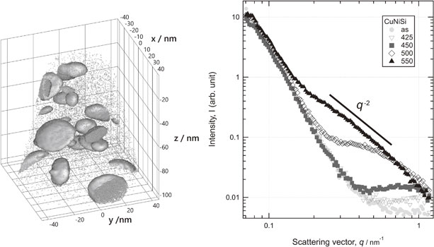
The SAXS and SANS results are shown in Figs. 3 and 4, respectively. The small-angle scattering profiles of the samples after solution treatment and heat-treatment at aging temperatures of 425, 450, 500 and 550°C are shown. Compared to the solution-treated sample, the profiles of the aging samples had a shoulder in the region of q between 0.2 and 2 nm−1, which demonstrates that the shoulder moves to the low-q side as the aging temperature increases. These results suggest that the Ni–Si precipitates are gradually coarsened.
3.3 Analysis of SAXS and SANS results
Since the SAXS profiles of the 425 and 450°C aging samples exhibit a q−4 slope, the Ni–Si precipitated phase can be interpreted as spherical, and we therefore performed curve fitting analysis using a model of spherical particles.7) The results showed that the simple average particle size was 2.2 nm for the 425°C aging sample and 2.6 nm for the 450°C aging sample, and the volume weighted average particle size was 2.6 nm for the 425°C aging sample and 3.5 nm for the 450°C aging sample. In contrast, the precipitated particle of the 500 and 550°C aging samples was not spherical due to the shape of the profiles. In addition, the background was high on the low-q side of q < 0.1 nm−1, which made analysis difficult. Therefore, we used the SANS profiles as a complement to analyze the scattering profile.
In the SAXS profiles of the 550 and 500°C aging samples in Fig. 3, the intensity decreases with the q−4 slope from the shoulder to the high-q side. In the SANS profiles, we can see that the intensity decreases with the q−2 slope from the Guinier region, which is characteristic of disk scattering.19) Since the precipitate appeared to be disk-shaped even in the TEM observation, we presumed it was a disk in the SANS analysis as well. Here, since the profile shapes of SAXS and SANS are different, we conclude that the Ni–Si precipitated phase is not a uniform phase particle but rather a core-shell particle, where the shell can be regarded as an interface diffusion layer between the core and parent phase. We tried to analyze these experimental results, but the SANS profile lacked high-q data and the background in the low-q side of the SAXS profile was high, which made it difficult to perform curve fitting as a disk shape. Therefore, the thickness of the disk was analyzed from the SAXS profile with the thickness plot, and the diameter of the disk was analyzed from the SANS profile with the Guinier plot.19) The results showed that the diameter of the disk was 6.1 nm for the 500°C aging sample and 12.0 nm for the 550°C aging sample. The thickness of the disk was 3.4 nm for the 500°C aging sample and 5.5 nm for the 550°C aging sample.
3.4 3DAP measurement
Figure 5 shows the 3DAP tomographic reconstruction of 500°C heat-treated copper alloy. In order to clearly visualize the diffusion layer, the figure shows the iso-concentration surface of 4 at% Si. We can see here that most of the precipitate sizes are several nm to 10 nm and have a slightly crushed shape rather than a spherical shape. In addition, we can confirm a precipitated phase with a size of about 50 nm. It took almost one day to perform the measurement, and we were able to measure with a large field of view (about 1 µm). The amount of data was 158 M atoms. We measured about 1000 precipitated phases, which enabled us to obtain sufficient statistics. The average volume of the precipitated phase defined by the iso-concentration surface of 2 at% Si was 446 nm3. In order to include most of the diffusion layers, the volume calculation was defined in terms of the iso-concentration surface of 2 at% Si.

For the 550°C aging sample, Fig. 6(a) shows the iso-concentration surface of 2 at% Si, where the precipitated phase is clearly visible. We can see that there is a wide precipitate size distribution of 5 to 20 nm. The 550°C aging sample was measured three times in volumes of approximately the same size. The average volume of the 30 precipitated phases defined by the iso-concentration surface of 2 at% Si was 1328 nm3. We selected one of these (shown in Fig. 6(b)) and created a line profile from it (Fig. 6(c)). From this line profile, we found that the composition ratio of Ni and Si in the central part of the precipitated phase was 2:1. This result is consistent with our interpretation that the precipitated phase was Ni2Si from the analysis of the electron diffraction pattern shown in Fig. 2. We can also confirm that a diffusion layer exists at the interface between the precipitated phase and the Cu parent phase. The thickness of the diffusion layer on the right side was about 4 nm, and the thickness of the precipitated phase containing the diffusion layer was 8 nm.

Next, we used the 3DAP results to proceed with the interpretation of the SANS and SAXS profiles. We calculated the possible scattering contrast of the diffusion layer in the Cu parent phase as shown in Fig. 7, where the diffusion layer is assumed to be δ (Ni1−y, Cuy)2Si following Yi et al.15) As we can see, the scattering contrast for X-rays does not significantly decrease even if the amount of Cu composition in the diffusion layer increases. On the other hand, the scattering contrast for neutrons decreases sharply as the Cu composition increases. This can be explained by the difference in scattering length between X-rays and neutrons.7) Specifically, since the X-ray scattering length monotonically increases as the atomic number increases, the effect on the scattering contrast is not significant even if the Ni and Cu of adjacent atomic numbers are substituted. On the other hand, the difference in the neutron scattering lengths between Ni and Cu is larger than that of X-rays since the neutron scattering length changes irregularly with respect to the atomic number. Therefore, the substitution of Ni and Cu has a large effect on the scattering contrast for neutrons. Due to these properties, the X-ray contrast does not significantly change even if Cu composition increases in the diffusion layer, and consequently, SAXS reflects the effect of both the diffusion layer and the core. At the same time, the neutron contrast decreases when the Cu composition increases, and as a result, neutron scattering from the diffusion layer weakens.

When we look again at Figs. 3 and 4, the slope from the shoulder is q−4 in the SAXS profile, which suggests that the precipitates are spherical or ellipsoidal. In SANS, the slope is q−2, suggesting that the precipitates are disk-shaped. Considering the scattering contrast discussed here, the precipitate shape is mostly ellipsoidal in SAXS because X-ray scattering reflects part of the diffusion layer. Since neutron scattering is less affected by the diffusion layer, the SANS results can be interpreted as reflecting the shape of the central disk. Figure 8 shows the core-shell model presumed from this analysis.

Next, we compare small-angle scattering and 3DAP analysis for the size of the precipitated phase. The average volume by 3DAP calculated in Section 3.4 was determined from the average volume defined by the iso-concentration surface of 2 at% Si including the diffusion layer. Therefore, we also need to consider the diffusion layer when calculating the volume from small-angle scattering. We calculated the diameter from the SANS Guinier plot, so the contribution of the Ni–Si core phase is dominant. That is, in the 550°C aging sample, the disk diameter of the core phase is 12 nm on average, and does not contain the diffusion layer. The average thickness of 5.5 nm calculated from the SAXS thickness plot is considered to include a part of the diffusion layer in addition to the Ni–Si core phase. That is, in the 550°C aging sample, a part of the thickness of the ellipsoid including the diffusion layer is considered to be 5.5 nm. Here, we calculated the average volume assuming that the diffusion layer was 2.8 nm because the layer was 2 to 4 nm in the 3DAP analysis. The average diameter is 17.6 nm when the diffusion layer thickness is 2.8 nm in the radial direction of the disk. We assumed that the disk thickness of 5.5 nm calculated by SAXS contains the thickness of 1.4 nm, which is half of the diffusion layer thickness of 2.8 nm.
On the basis of the above assumptions, we calculated the average volume of ellipsoidal precipitates from small-angle scattering. In the 550°C aging sample, the average volume of the precipitate was 1362 nm3. In the 500°C aging sample, it was 436 nm3. These results show good agreement with the average volume of the precipitated phase calculated by 3DAP. However, to ensure greater precision, it will be necessary to create a diffusion layer model that includes the Si composition change at the interface between the Cu parent phase and the Ni–Si precipitated phase. We leave this to future work.
4. Conclusion
Our main findings in this study are as follows.
-
(1)
SAXS and SANS measurements show that the precipitated phase becomes coarser as the aging temperature rises. The SAXS profile suggested that the precipitate was an ellipsoid, and the SANS suggested it was a disk.
-
(2)
By using ultraviolet laser-assisted field evaporation in the 3DAP measurement, it becomes possible to measure a copper alloy over a stable and wide area. There also seems to be a diffusion layer at the interface between the precipitated phase and the Cu parent phase.
-
(3)
Considering the combined analysis results of TEM, SAXS, SANS, and 3DAP, a disk-shaped Ni2Si exists in the center of the precipitated phase in the 550 and 500°C aging samples. There is a diffusion layer at the interface between the precipitation and the Cu parent phase. The shape of the precipitated phase, including the diffusion layer, is considered to be ellipsoid.
-
(4)
The various analytical methods presented in this paper can also be applied to the analysis of fine precipitated phases in other copper alloys, and useful for clarifying material properties.
Acknowledgments
STEM observation was supported by the University of Tokyo Advanced Characterization Nanotechnology Platform in the Nanotechnology Platform Project sponsored by the Ministry of Education, Culture, Sports, Science and Technology (MEXT), Japan. Laboratory-SAXS measurements were carried out jointly with the Institute for Integrated Radiation and Nuclear Science, Kyoto University. SAXS measurements in SPring-8 were performed at Hyogo Prefecture Beamline BL08B2 with the cooperation of Mr. Shigeo Kuwamoto of the Hyogo Science and Technology Association (Proposal No. 2019A3337). SANS measurements were performed at Ibaraki Neutron Beamline BL20 iMATERIA in the MLF facility at J-PARC (Proposal No. 2018BM0019). Three-dimensional atom probe measurements were performed at the NIMS-CAMECA 3DAP laboratory.
REFERENCES
- 1) S.A. Lockyer and F.W. Noble: J. Mater. Sci. 29 (1994) 218–226. doi:10.1007/BF00356596
- 2) H. Fujiwara, T. Sato and A. Kamio: J. Japan Inst. Metals 62 (1998) 301–309 (in Japanese). doi:10.2320/jinstmet1952.62.4_301
- 3) A. Araki, E. Kobayashi, T. Sato, K. Hirose and T. Eguchi: J. Japan Inst. Copper 52 (2013) 14–18 (in Japanese).
- 4) Q. Lei, Z. Li, C. Dai, J. Wang, X. Chen, J.M. Xie, W.W. Yang and D.L. Chen: Mater. Sci. Eng. A 572 (2013) 65–74. doi:10.1016/j.msea.2013.02.024
- 5) Y. Jia, M. Wang, C. Chen, Q. Dong, S. Wang and Z. Li: J. Alloy. Compd. 557 (2013) 147–151. doi:10.1016/j.jallcom.2012.12.154
- 6) A. Araki, W.J. Poole, E. Kobayashi and T. Sato: Mater. Trans. 55 (2014) 501–505. doi:10.2320/matertrans.MBW201326
- 7) M. Ohnuma: Materia Japan 54 (2015) 616–620 (in Japanese). doi:10.2320/materia.54.616
- 8) M. Ohnuma, J. Suzuki, S. Ohtsuka, S.W. Kim, T. Kaito, M. Inoue and H. Kitazawa: Acta Mater. 57 (2009) 5571–5581. doi:10.1016/j.actamat.2009.07.054
- 9) Y. Oba: Bull. Iron Steel Inst. Japan (Ferrum) 18 (2013) 257–259 (in Japanese).
- 10) Y. Oba, S. Koppoju, M. Ohnuma, T. Murakami, H. Hatano, K. Sasakawa, A. Kitahara and J. Suzuki: ISIJ Int. 51 (2011) 1852–1858. doi:10.2355/isijinternational.51.1852
- 11) T. Miyazawa, Y. Tanaka and T. Fujii: J. Japan Inst. Copper 58 (2019) 103–107 (in Japanese).
- 12) H. Sasaki, T. Isomatsu, M. Higuchi, Y. Oba and M. Ohnuma: Abst. 58th Conf. Japan Inst. Copper, (2018) pp. 27–28 (in Japanese).
- 13) H. Karino, T. Sato, K. Hirose and T. Eguchi: J. Japan Inst. Copper 45 (2006) 115–119 (in Japanese).
- 14) S. Lee, H. Matsunaga, X. Sauvage and Z. Horita: Mater. Charact. 90 (2014) 62–70. doi:10.1016/j.matchar.2014.01.006
- 15) J. Yi, Y. Jia, Y. Zhao, Z. Xiao, K. He, Q. Wang, M. Wang and Z. Li: Acta Mater. 166 (2019) 261–270. doi:10.1016/j.actamat.2018.12.047
- 16) H. Sasaki, T. Matusda, T. Kato, T. Muroga, Y. Iijima, T. Saitoh, F. Iwase, Y. Yamada, T. Izumi, Y. Shiohara and T. Hirayama: J. Electron Microsc. 53 (2004) 497–500. doi:10.1093/jmicro/dfh067
- 17) H. Sasaki, T. Kato, T. Matusda and T. Hirayama: Kenbikyo 46 (2011) 188–194 (in Japanese). doi:10.11410/kenbikyo.46.3_188
- 18) T. Ohkubo, Y. Chen, K. Kodzuka and K. Hono: Materia Japan 50 (2011) 397–403 (in Japanese). doi:10.2320/materia.50.397
- 19) H. Matsuoka: J. Cryst. Soc. Jpn. 41 (1999) 213–226 (in Japanese). doi:10.5940/jcrsj.41.213