特集「ナノスケール3次元分析の最前線」
集束イオンビームと電子顕微鏡を用いた3次元構造評価
2018 年 61 巻 12 号 p. 772-777
詳細
2018 年 61 巻 12 号 p. 772-777
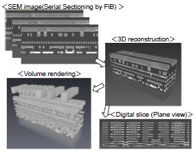
Recently, latest semiconductor devices have three-dimensional (3D) structure and nanostructured materials have 3D distribution of its components. Therefore, 3D analysis methods are required. In this report, some cases that were analyzed using serial sectioning method and TEM tomography method are introduced.