特集「表面洗浄技術」
マイクロバブルを利用した半導体ウエハの洗浄技術
2018 年 61 巻 2 号 p. 64-69
詳細
2018 年 61 巻 2 号 p. 64-69
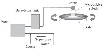
Semiconductor cleaning is a very important process in integrated circuit manufacturing, and the removal of high dose ion implanted photoresist is a big challenge in semiconductor cleaning owing to their carbonized crust layer generated on and near the surface of the photoresist layer. Microbubbles are a promising candidate in single wafer spin cleaning process for the removal of the crust generated photoresist without any substrate loss. And the bubbles are gas bodies less than 50 micrometer in diameter and shrink underwater due to the rapid dissolution of the interior gas. It has been demonstrated that the bubbles can generate free radicals during the collapsing process under water through the dispersion of the elevated energy accumulated as the surface electricity during the collapsing process of microbubble. In this article the author introduces the fundamental properties of microbubble and their several examples relating to semiconductor cleaning.