特集「2018年日本表面真空学会学術講演会特集号II」
原子層制御したシリコン三次元立体表面構造の創製・観察技術
2019 年 62 巻 7 号 p. 427-432
詳細
2019 年 62 巻 7 号 p. 427-432
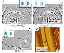
We have established the original methodology that enable to observe atomic orderings and arrangements of “surfaces with arbitrary directions” on 3D figured structures, by developing diffraction and microscopy techniques. An original technique, namely, the directly and quantitatively viewing of the side- and facet-surfaces in atomic scale using reflection high-energy electron diffraction (RHEED) and scanning tunneling microscope (STM), can feedback to the determination of process parameters in the etching procedure. The scientifically optimized etching recipe enabled the creation of atomically-ordered side-surfaces, which are perpendicular to planar substrate surfaces on 3D patterned Si substrates. RHEED and STM prove atomically-reconstructed Si{100}2×1, {110}16×2, and {111}7×7 side-surfaces that were realized for the first time. We have also developed the atomically-ordered 3D nanofabrication technique, where the material stacking direction is switched from the general out-of-plane to in-plane direction, and realized the formation ultra-thin epitaxial films in 3D space.