All issues

Successor
Volume 34, Issue 5
Displaying 1-12 of 12 articles from this issue
- |<
- <
- 1
- >
- >|
Preface
-
Katsumi URA2013 Volume 34 Issue 5 Pages 225
Published: May 10, 2013
Released on J-STAGE: May 18, 2013
JOURNAL FREE ACCESSDownload PDF (195K)
Special Issue: Frontiers of Aberration-Corrected Atomic Scale Electron Microscopy
-
Kunio TAKAYANAGI, Yoshifumi OSHIMA, Soyeon LEE, Takayuki TANAKA, Yasum ...Article type: Review
2013 Volume 34 Issue 5 Pages 226-233
Published: May 10, 2013
Released on J-STAGE: May 18, 2013
 JOURNAL FREE ACCESSAberration corrected electron microscopy has revealed various aspects of materials and their functions, i.e., interfacial, ionic, chemical, photonic, plasmonic, magnetic and electronic aspects. A 50 pm resolution microscopy, particularly, enabled us to observe lithium ions in LiMn2O4, a material used as lithium ion battery electrodes. The 50 pm electron probe scanning over the surface is sensitive enough to detect a single adatom/vacancy similarly to STM. The 50 pm microscopy, in transmission mode of observation, is useful for study of catalysis, as demonstrated for Au/TiO2 in O2 and/or CO environment. Aberration corrected in-situ electron microscopy provides atomic, ionic, and electronic properties, in relation to structures at “nano in macro”.View full abstractDownload PDF (1522K)
 -
Eric VAN CAPPELLEN, Alex BRIGHT, Joerg R. JINSCHEK, Koji INOKE, Bert F ...Article type: Current Topic
2013 Volume 34 Issue 5 Pages 234-239
Published: May 10, 2013
Released on J-STAGE: May 18, 2013
 JOURNAL FREE ACCESSAlthough developed to improve spatial resolution, a TEM spherical aberration corrector or ‘image corrector’ has the added benefit of eliminating the artifact of delocalization in HR-TEM imaging. This greatly increases the power of HRTEM imaging and is especially important for clear imaging of surfaces and interfaces. When such a corrector is combined with a source monochromator, ultra high resolution at low accelerating voltages also becomes feasible. These technologies can also be added to an environmental TEM (ETEM) to achieve unprecedented resolution on TEM samples in gaseous environments. Some recent results illustrating the power of image corrected TEM and how it is being used at the cutting edge of materials science are presented.View full abstractDownload PDF (1325K)
 -
Hidetaka SAWADA, Takeo SASAKI, Eiji OKUNISHI, Kazutomo SUENAGAArticle type: Current Topic
2013 Volume 34 Issue 5 Pages 240-246
Published: May 10, 2013
Released on J-STAGE: May 18, 2013
 JOURNAL FREE ACCESSThe geometrical limitations of resolution caused by third-order spherical aberration were overcome with the development of practical aberration correctors. Spherical aberration correctors for probe-forming systems have been widely used in high-resolution structural and analytical studies. The performance of the microscope at medium acceleration voltages was sufficiently improved for resolving the atomic position and performing chemical analysis on an atomic level. We demonstrated that a low voltage microscope had the ability to facilitate atomic-resolution imaging and analytical study.View full abstractDownload PDF (2359K)
 -
Hiromi INADA, Keiji TAMURA, Yuya SUZUKI, Takahiro SATO, Mitsuru KONNO, ...Article type: Current Topic
2013 Volume 34 Issue 5 Pages 247-252
Published: May 10, 2013
Released on J-STAGE: May 18, 2013
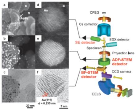 JOURNAL FREE ACCESSWe innovated the secondary electron (SE) imaging technology with an aberration-corrected scanning transmission electron microscope (STEM). As a result, atomic resolution SE imaging has been achieved for the first time. We have successfully observed isolated single uranium atoms on carbon thin films using the SE signal. In addition, atomic-resolutionSE images were obtained not only from specimens containing heavy elements like uranium but also from those composed of light elements such as silicon and carbon. Because the SE signals are from the upper surface of specimen, imaging atomic lattice for thick specimens of 1 µm was demonstrated. This unique technology provides unprecedented application capabilities including 1) simultaneous atomic-resolution SE/STEM imaging to reveal topographical surface and bulk structure ; 2) simplified specimen preparation requirement for atomic-resolution electron microscopy ; and 3) imaging atomic structure for thicker than 1 µm specimens without having to use a million volt electron microscope.View full abstractDownload PDF (1166K)
 -
Naoya SHIBATA, Yuichi IKUHARAArticle type: Current Topic
2013 Volume 34 Issue 5 Pages 253-258
Published: May 10, 2013
Released on J-STAGE: May 18, 2013
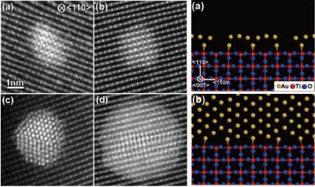 JOURNAL FREE ACCESSAberration-corrected scanning transmission electron microscopy (STEM) is becoming a very powerful tool to directly characterize defect structures in materials and devices at atomic dimensions. Here, we review our recent researches on material interface characterization using STEM. First example is that the direct imaging of individual dopant atoms within a buried alumina interface. The second example is the atomic-scale characterization of Au nanoislands on TiO2 substrates. The ability to directly probe individual atoms within buried interfaces at very high-resolution will significantly assists our understanding of interface structures and related properties in many advanced materials and devices.View full abstractDownload PDF (1466K)
 -
Tomoki AKITA, Noboru TAGUCHI, Masanori KOHYAMAArticle type: Current Topic
2013 Volume 34 Issue 5 Pages 259-264
Published: May 10, 2013
Released on J-STAGE: May 18, 2013
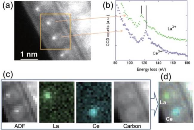
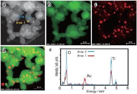 JOURNAL FREE ACCESSAberration corrected TEM/STEM was applied for the observations of functional materials for environmental and energy devices. Some experimental results are presented in this brief report. High resolution transmission electron microscopy (HRTEM) and high angle annular dark field scanning transmission electron microscopy (HAADF-STEM) observations were carried out for Au on metal oxide catalysts in order to observe fine structure of Au particle and the interface between Au and metal oxide. Elemental mapping by energy dispersive X-ray spectroscopy (EDS) was also examined for Au/TiO2 catalyst, and the distribution of Au particles was obtained in nano-scale. Electrode materials for Lithium ion batteries were also observed by STEM and electron energy loss spectroscopy (EELS). STEM-EELS spectrum imaging was performed for the Li1.2Mn0.4Fe0.4O2 positive electrode with high energy resolution using monochrometer. It enables us to estimate oxidation state of transition metals by energy loss near edge structure (ELNES).View full abstractDownload PDF (1767K)
Original
-
Ken KOYAMAArticle type: Original
2013 Volume 34 Issue 5 Pages 265-267
Published: May 10, 2013
Released on J-STAGE: May 18, 2013
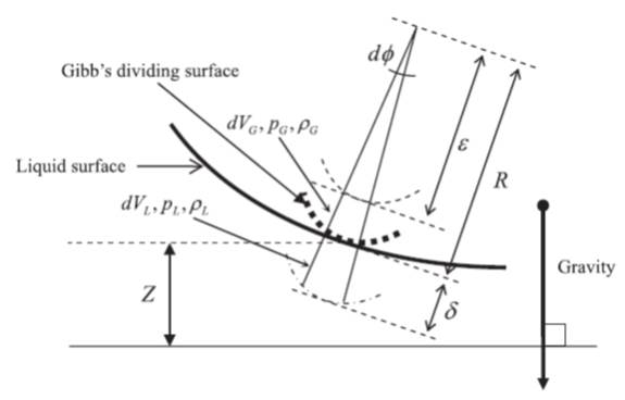 JOURNAL FREE ACCESSIn this paper, examination thermodynamic about the geometric form of the surface under gravitational attraction was performed. First, the conventional method based on a Laplace equation was reconsidered, and the point in question accepted from a viewpoint of continuum mechanics was clarified to how to catch the pressure of a liquid and gas. Such a problem did not arise in the thermodynamic approach, but the result containing the conventional result according to a Laplace equation was obtained.View full abstractDownload PDF (268K)
Planning Series
Surface Science for Energy Issues
-
Yoshihiro MURAI2013 Volume 34 Issue 5 Pages 268-270
Published: May 10, 2013
Released on J-STAGE: May 18, 2013
 JOURNAL FREE ACCESSDownload PDF (1590K)
Science Café
Research Abroad
-
Masaya TODA2013 Volume 34 Issue 5 Pages 271-272
Published: May 10, 2013
Released on J-STAGE: May 18, 2013
JOURNAL FREE ACCESSDownload PDF (670K)
Report of International Symposium
-
Ryan Lacdao AREVALO, Elvis Flaviano ARGUELLES, Hideaki KASAI2013 Volume 34 Issue 5 Pages 273-274
Published: May 10, 2013
Released on J-STAGE: May 18, 2013
 JOURNAL FREE ACCESSDownload PDF (636K)
News & Trends
-
2013 Volume 34 Issue 5 Pages 275
Published: May 10, 2013
Released on J-STAGE: May 18, 2013
JOURNAL FREE ACCESSDownload PDF (190K)
- |<
- <
- 1
- >
- >|