All issues
Successor
Volume 35, Issue 2
Displaying 1-12 of 12 articles from this issue
- |<
- <
- 1
- >
- >|
Preface
-
(Collaboration of Science, Technology and Engineering)Hiroyuki MATSUNAMI2014 Volume 35 Issue 2 Pages 73
Published: February 10, 2014
Released on J-STAGE: February 19, 2014
JOURNAL FREE ACCESSDownload PDF (197K)
Special Issue: Wide Bandgap Semiconductors for Power Devices and Their Surface Science
-
Osamu ERYU, Yayoi TANAKAArticle type: Current Topic
2014 Volume 35 Issue 2 Pages 74-77
Published: February 10, 2014
Released on J-STAGE: February 19, 2014
 JOURNAL FREE ACCESSWe made an off-axis surface of SiC with the chemical-mechanical polishing (CMP) method to examine the influence of an atomic step on the electronic properties. It became clear that processing pressure had the threshold in the electric field that let the removal of the atom accelerate using the abrasive of the piezoelectric particles. The electric charge distribution of the SiC surface affects the removal rate of SiC. The conductive atomic force microscopy (CAFM) method is effective technique to examine processing mechanism of the materials surface.View full abstractDownload PDF (438K)
 -
Kazutoshi KOJIMA, Keiko MASUMOTO, Sachiko ITO, Akiyo NAGATA, Hajime OK ...Article type: Current Topic
2014 Volume 35 Issue 2 Pages 78-83
Published: February 10, 2014
Released on J-STAGE: February 19, 2014
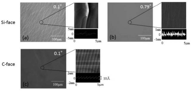 JOURNAL FREE ACCESSWe investigated homoepitaxial growth on 4H-SiC substrates with a vicinal off-angle lower than 1°. The small off angle difference of a tenth part of a degree has an influence on surface morphology of epitaxial layers. This tendency also depends on the face polarity and a C-face can be obtained that has a specular surface with a lower vicinal off angle than a Si-face. Low C/Si ratio conditions are also important to control the surface morphology of these substrates. Especially, controlling C/Si ratio with SiH4 flow rate is effective to suppress the generation of step bunching on Si-face epitaxial layers. These results indicate the control of surface free energy is also important to controlling the surface morphology of homoepitaxial growth on these substrates.View full abstractDownload PDF (714K)
 -
Yukihiko WATANABE, Takashi KATSUNO, Tsuyoshi ISHIKAWA, Hirokazu FU ...Article type: Current Topic
2014 Volume 35 Issue 2 Pages 84-89
Published: February 10, 2014
Released on J-STAGE: February 19, 2014
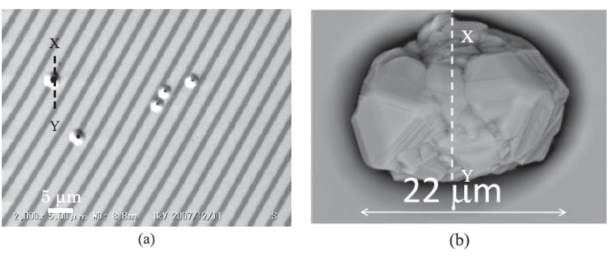 JOURNAL FREE ACCESSThe good relations between the reverse characteristics of 4H-SiC JBS diodes and the surface defects were obtained. The reverse characteristics of 4H-SiC JBS diodes were categorized in three groups as follows : (A) low blocking voltage, (B) high leakage current and (C) low leakage current. The groups of (A) and (B) were caused by the existences of the micropipe and small particles, and the carrot-like defects on the SiC surfaces, respectively. In group (C), nanosized circular cone shaped pits (nanopits) were observed at the leakage current sources. The positions of nanopits corresponded to the positions of threading dislocations.View full abstractDownload PDF (1331K)
 -
Hiroshi YANO, Tomoaki HATAYAMA, Takashi FUYUKIArticle type: Current Topic
2014 Volume 35 Issue 2 Pages 90-95
Published: February 10, 2014
Released on J-STAGE: February 19, 2014
 JOURNAL FREE ACCESSWe have developed a new technique, POCl3 annealing, to improve 4H-SiC MOS interface properties. In this paper effects of phosphorus incorporation into the gate oxide by POCl3 annealing on electrical properties of 4H-SiC MOS devices are introduced. POCl3 annealing is more effective to reduce interface state density (Dit) and near-interface traps (NITs), and to improve channel mobility compared with the conventional NO annealing. High-low C-V characteristics at room temperature, cyclic C-V characteristics at 80 K, and thermal stimulated current measurements for MOS capacitors revealed that most of Dits near the conduction band edge and NITs are greatly reduced to the detection limit level. I-V characteristics of MOSFETs showed that the channel mobility was improved to be 89 cm2/Vs, which is 3 times higher than that of the NO annealed MOSFETs. Chemical bond structures at the interface for NO and POCl3 annealed samples are also investigated by X-ray photoelectron spectroscopy.View full abstractDownload PDF (1031K)
 -
Tamotsu HASHIZUME, Zenji YATABE, Taketomo SATOArticle type: Current Topic
2014 Volume 35 Issue 2 Pages 96-101
Published: February 10, 2014
Released on J-STAGE: February 19, 2014
 JOURNAL FREE ACCESSInterface properties of GaN-based heterostructures have been characterized. Schottky contacts on dry-etched n-GaN layers showed leaky I-V characteristics. An anneal process at 400°C was effective in recovering the rectifying characteristics. To characterize interface properties of Al2O3 insulated gates on AlGaN/GaN structures with and without the inductively coupled plasma (ICP) etching of AlGaN, we have developed a C-V calculation method taking into account electronic state charges at the Al2O3/AlGaN interface and a photoassisted C-V technique utilizing photons with energies less than the bandgap of AlGaN. It was found that the ICP etching caused the monolayer-level interface roughness, disorder of the chemical bonds and formation of various types of defect complexes at the AlGaN surface, resulting in poor C-V characteristics due to high-density interface states at the Al2O3/AlGaN interface.View full abstractDownload PDF (1873K)
 -
Masataka HIGASHIWAKI, Kohei SASAKIArticle type: Current Topic
2014 Volume 35 Issue 2 Pages 102-107
Published: February 10, 2014
Released on J-STAGE: February 19, 2014
 JOURNAL FREE ACCESSGallium oxide (Ga2O3) has excellent material properties for power device applications represented by the extremely large breakdown field due to a large bandgap of 4.7-4.9 eV. Another important feature in industry is that large single-crystal β-Ga2O3 bulks and wafers can be fabricated with melt-growth methods. We recently succeeded in fabricating Ga2O3 metal-oxide-semiconductor field-effect transistors (MOSFETs) by using newly developed technologies for making single-crystal bulks, growing conductivity-controlled epitaxial films, and fabricating devices. The MOSFETs exhibited excellent device characteristics including an off-state breakdown voltage over 370 V, an extremely low leakage current, and a high on/off drain current ratio of more than ten orders of magnitude. These results indicate that Ga2O3 have comparable or even more potential than Si and typical widegap semiconductors SiC and GaN for power device applications.View full abstractDownload PDF (1308K)
 -
Kenji SHIRAISHIArticle type: Current Topic
2014 Volume 35 Issue 2 Pages 108-113
Published: February 10, 2014
Released on J-STAGE: February 19, 2014
 JOURNAL FREE ACCESSWe have investigated the interfaces of wide gap semiconductors by using first principles calculations. We show that oxidation of SiC induces the formation of C-C bond defects at SiC/SiO2 interfaces which corresponds to the oxidation front of SiC. We also find that this C-C bond formation leads to the formation of shallow interface states near the SiC conduction band bottoms. Moreover, we clarify the mechanism of hole generation on H-terminated diamond surfaces by the adsorption of molecules whose lowest unoccupied molecular orbital (LUMO) levels or single occupied molecular orbitals (SOMO) levels are located lower than the valence band top of H-terminated diamonds.View full abstractDownload PDF (895K)
Planning Series
Surface Science for Resource Issues
-
Koji HIRAI2014 Volume 35 Issue 2 Pages 114-115
Published: February 10, 2014
Released on J-STAGE: February 19, 2014
 JOURNAL FREE ACCESS
Science Café
Research Abroad
-
Hiroki WADATI2014 Volume 35 Issue 2 Pages 116-117
Published: February 10, 2014
Released on J-STAGE: February 19, 2014
JOURNAL FREE ACCESSDownload PDF (531K)
Qualifying Examination for Surface Science Engineers
-
2014 Volume 35 Issue 2 Pages 118
Published: February 10, 2014
Released on J-STAGE: February 19, 2014
JOURNAL FREE ACCESSDownload PDF (1675K)
News & Trends
-
2014 Volume 35 Issue 2 Pages 119
Published: February 10, 2014
Released on J-STAGE: February 19, 2014
JOURNAL FREE ACCESSDownload PDF (192K)
- |<
- <
- 1
- >
- >|