
- |<
- <
- 1
- >
- >|
-
金原 粲2017 年 38 巻 5 号 p. 209
発行日: 2017/05/10
公開日: 2017/05/21
ジャーナル フリーPDF形式でダウンロード (144K)
-
 勝沼 隆幸, 久松 亨, 木原 嘉英, 本田 昌伸原稿種別: 研究紹介
2017 年 38 巻 5 号 p. 210-215
発行日: 2017/05/10
公開日: 2017/05/21
 ジャーナル フリー
We introduce a state-of-the-art patterning process developed by new patterning technology using Atomic Layer Deposition (ALD) towards 5/7 nm generation. In the patterning process, critical dimension (CD) shrink technique without CD loading is one of the key requirements. However, in the conventional CD shrink technique, CD loading canʼt be solved in principle. To overcome this issue, by integrating ALD process into the etching flow, we developed a new CD shrink technique without causing CD loading. Furthermore, CD shrink amount can be precisely controlled by the number of ALD cycles while keeping the excellent CD shrink uniformity across a wafer. This is obtained by utilizing a conformal layer with characteristics of ALDʼs self-limiting reaction, which is independent of the pattern variety.
抄録全体を表示Editor's pickPDF形式でダウンロード (1195K) -
大西 剛原稿種別: 研究紹介
2017 年 38 巻 5 号 p. 216-221
発行日: 2017/05/10
公開日: 2017/05/21
 ジャーナル フリーReproducible way to grow high quality complex oxide thin films by means of pulsed laser deposition is addressed. Laser ablation conditions are the most essential ones to be controlled precisely because it directly relates to cation ratio of deposited thin films. In some specific case, substrate temperature and gas pressure also become important to control the film composition. Film quality is tightly correlated to the thin film stoichiometry.抄録全体を表示PDF形式でダウンロード (1213K)
 -
三成 剛生, Xuying LIU, 金原 正幸原稿種別: 研究紹介
2017 年 38 巻 5 号 p. 222-227
発行日: 2017/05/10
公開日: 2017/05/21
 ジャーナル フリーFully printed electronics on plastic have attracted considerable interest owing to their high compatibility and ease of integration. Here, we developed an ultra-high-resolution printing technique based on “surface selective deposition” that can deposit functional inks with 1-μm resolution on flexible substrates. We used this technique to selectively deposit a metal nanoparticle ink and an organic semiconducting material, thereby allowing the large-scale fabrication of high-resolution electronic circuits including organic thin-film transistors with channels as short as 1 μm under ambient atmosphere. We also developed π-junction gold nanoparticles as the electrode material which permitted room-temperature deposition of a conductive metal layer. The room-temperature process enables printing of electronic circuits without application of heat, thus thermal damage to the substrate can be totally avoided. These results indicate that this bottom-up fabrication method based on fluidic self-assembly is promising for the fabrication of large-area, high-resolution, low-cost electronics.抄録全体を表示PDF形式でダウンロード (990K)
 -
中野 武雄原稿種別: 研究紹介
2017 年 38 巻 5 号 p. 228-233
発行日: 2017/05/10
公開日: 2017/05/21
 ジャーナル フリー
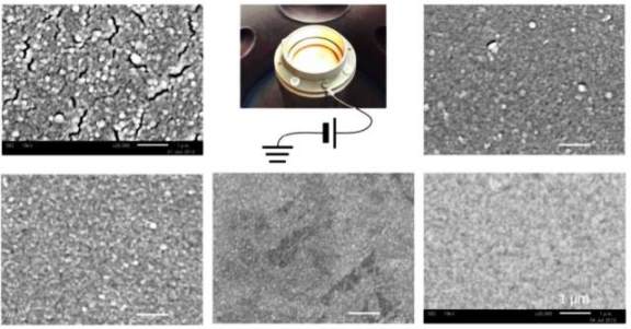
High power pulsed magnetron sputtering (HPPMS) is a variant of sputtering deposition method in that pulsed power is applied to the sputtering target with low repetition frequency and small duty ratio. It produces high density plasma intermittently which enables the ionization of sputtered atoms and the control of their energy and direction by introducing potential difference between the plasma and the substrate. We have proposed two HPPMS techniques which can control the plasma potential. One is to modify the target voltage waveform where the positive voltage is applied during the “pulse-off” period. The other is to use the triode configuration in which a positively-biased electrode is added. Positive plasma potential could be confirmed experimentally, and dense film structures and smooth surfaces could be obtained by these methods. It suggested that the ionized atoms impinged on the growing film surface with accelerated kinetic energy.
抄録全体を表示PDF形式でダウンロード (989K) -
大平 圭介, Trinh Cham THI, 及川 貴史, 瀨戸 純一, 小山 晃一, 松村 英樹原稿種別: 研究紹介
2017 年 38 巻 5 号 p. 234-239
発行日: 2017/05/10
公開日: 2017/05/21
 ジャーナル フリー
Back-contact c-Si solar cells can realize superior performance due to no shadowing loss. Surface passivation with excellent quality is required for achieving sufficient conversion efficiency in the back-contact cells. Cat-CVD can produce high-quality passivation films owing to its plasma-damage-less nature. SiNx deposition at a low temperature and successive post annealing leads to a surface recombination velocity (SRV) of < 5 cm/s. The exposure of c-Si wafers to catalytically generated phosphorus radicals can form ultra-thin highly-doped layers (Cat-doping). This P-doped region acts to reduce an SRV to < 2 cm/s by combining with a Cat-CVD SiNx film. We have also established the passivation of rear c-Si surfaces by Cat-CVD a-Si with suppressing epitaxial growth by introducing ultra-thin oxide layers formed by dipping in H2O2. The formation of doped a-Si by Cat-doping has also been demonstrated, which will be applicable to the formation of patterned doping regions in Si heterojunction back-contact cells.
抄録全体を表示PDF形式でダウンロード (1000K) -
鹿毛 剛原稿種別: ポピュラーサイエンス
2017 年 38 巻 5 号 p. 240-243
発行日: 2017/05/10
公開日: 2017/05/21
 ジャーナル フリー
The unique properties of diamond like carbon (DLC) film, including its chemical inertness and impermeability, make it possible for new applications in food and beverage. In this paper, I summarize and review the recent progress of gas barrier enhancement of polyethylene terephthalate (PET) bottles for beverage from the view point of the application of DLC coating. A unique technique of plasma CVD method has been developed to deposit DLC layer on the inside surface of PET bottles. The DLC-coated PET bottle exhibits extremely high gas barrier properties against oxygen, carbon dioxide and flavors compared to conventional bottles. For the practical use of PET bottles as a commodity, machines have been introduced for soft drink, wine, Japanese sake, edible oil, seasonings and others.
抄録全体を表示PDF形式でダウンロード (578K)
-
木下 稔夫2017 年 38 巻 5 号 p. 244-246
発行日: 2017/05/10
公開日: 2017/05/21
 ジャーナル フリー
「漆器」は,日本を代表する工芸品だが,バブル崩壊後の漆器業界は,国民の生活様式の変化や消費者ニーズに適応した商品開発の遅れなどにより生産額,企業数,従業員数いずれも減少が続いている。そこで本稿では,現代の生活様式に対し,扱いやすい「漆器」を実現するために素地に着目し,従来の伝統的漆器に用いられていた「漆」と「木」という天然の原料のみを用いながら,漆器素地を製造できる成形材料開発を行ったので紹介を行う。
抄録全体を表示PDF形式でダウンロード (757K)
-
坂田 智裕2017 年 38 巻 5 号 p. 247-248
発行日: 2017/05/10
公開日: 2017/05/21
ジャーナル フリーPDF形式でダウンロード (400K)
-
 ジャーナル フリーPDF形式でダウンロード (196K)
 -
藤川 安仁2017 年 38 巻 5 号 p. 250
発行日: 2017/05/10
公開日: 2017/05/21
 ジャーナル フリーPDF形式でダウンロード (269K)
-
2017 年 38 巻 5 号 p. 251
発行日: 2017/05/10
公開日: 2017/05/21
ジャーナル フリーPDF形式でダウンロード (168K)
- |<
- <
- 1
- >
- >|