Abstract
Microelectrodes for hydrogen permeation measurements were fabricated by photolithography. Although the application of a positive-type photoresist coating was effective for the formation of a circle-shaped pattern with a diameter of several tens of micrometers on an iron surface, the coating had poor adhesion to the iron surface and poor durability in an H2SO4 solution. However, the addition of a silica coating derived from tetraethoxysilane (TEOS) on the iron surface as an inner layer resulted in improvement of durability as well as resistance of the coating. Furthermore, the introduction of a layer derived from a mixture of TEOS and glycidyl 3-trimethoxysilylpropyl ether (GPTMS) between the inner layer derived from TEOS and the photoresist coating resulted in long durability showing a large impedance of more than 109 Ω cm2 for 4×10⁵ s in an H2SO4 solution. Cathodic polarization of the microelectrode on the iron surface revealed that the hydrogen evolution reaction (HER) rate is dependent on the plane orientation of the surface. HER rate on an SCM435 steel surface also strongly depended on the microstructure and hardness of the local surface.
1. Introduction
Hydrogen embrittlement (HE) is one of important issues of structural materials because it is related to stress corrosion cracking, which significantly shortens the lifetime of a structure. In order to establish effective ways to prevent HE, it is necessary to clarify the mechanism of hydrogen permeation into the material that occurs simultaneously with a hydrogen evolution reaction (HER). Five years ago, a report titled “Comprehensive Understanding of Hydrogen-Passive Surface on Steels for Prevention of Hydrogen Embrittlement” based on the results of several studies was published by an ISIJ working group.1) In one of those studies, we developed a new method for local measurement of hydrogen permeation into a steel sheet using a micro-capillary technique applied to a Devanathan-Stachurski electrochemical (DS) cell.2) An electrolyte-flowing design for the hydrogen entry side of the DS cell enabled detection of hydrogen permeation responses on a hydrogen exit side electrode in a microcapillary cell with a diameter of 250 μm. It was found that the phase shift of the detected permeation current from a sinusoidal perturbation of the electrolyte flow rate in the hydrogen entry cell was strongly dependent on the metallographic structure of the steel sheet. A local structure in which two grains form a grain boundary led to hydrogen permeation more frequently than a local structure of each grain, suggesting that the diffusion coefficient of the boundaries was at least two-times larger than that of the grains. However, it was difficult to flow the electrolyte in the microcapillary and to carry out local hydrogen permeation measurement in which a microcapillary is used for the hydrogen entry side. It was also difficult to improve the spatial resolution of the technique even in the original design, in which a microcapillary is used for the hydrogen exit side, because of the difficulty in setting a smaller microcapillary in the DS cell.
However, improvement in the spatial resolution of hydrogen permeation measurements has been desired since it is thought that the hydrogen entry reaction strongly depends on the metallographic structure of the entry surface as well as the presence of oxide and inhibitors. In order to realize a local hydrogen entry reaction with a fine resolution and finally to apply it to the DS cell for hydrogen permeation measurement, the development of a state-of-the-art method like the egg in the Columbus story is necessary. Photolithography has been a conventional technique for fabricating microstructures on surfaces and has been used in various fields, especially in electronics. Microelectrodes have also been fabricated by photolithography and used for microelectrochemistry of the surfaces of materials. Kudelka et al. studied anodic oxidation behaviors of polycrystalline titanium3,4) and zirconium4) using microelectrodes fabricated by a positive-type photoresist coating and the so-called nL-droplet method, in which the electrode surface was limited to the area contacted with an electrolyte droplet. Jin et al. also used type-2205 duplex stainless steel microelectrodes fabricated by photolithography for microelectrochemical measurements using a microcapillary cell and reported corrosion behavior depending on the microstructure.5) Recently, we reported the HER on an Al–Si alloy strongly depended on the composition of Si in the microelectrode surface that was fabricated by photolithography using a positive-type photoresist.6) As discussed here, however, the photoresist coating has poor adhesion and a low resistance against electrolyte immersion and electrochemical measurements when the coating is used as an insulating material for an electrode.
In this work, photolithography with a positive-type photoresist was used for the fabrication of steel microelectrodes. In order to improve adhesion and resistance of the resist coating, an inner layer of silica was introduced under the coating and applied to an electrode-fabricating insulator for polarization of steel microelectrodes. The fabricated steel microelectrodes were used for cathodic polarization measurements of HER, which is partly an initial process of the hydrogen permeation reaction.
2. Experimental
An iron sheet (99.99 mass% Fe) with a thickness of 2 mm was used as a specimen for photolithography, and an SCM435 steel rod (Fe-0.35% C-0.18% Si-0.74% Mn-0.0011% P-0.0017% S-1.15% Cr-0.15% Mo) was used as a specimen for hydrogen permeation measurement. The rod with an original diameter of 60 mm was heated at 1123 K for 7.2 ks, cooled in an oil bath, re-heated at 803 K for 10.8 ks, and cooled in air. After the heating, the rod was cut into 1-mm-thick disks and mechanically polished finally using colloidal silica particles of 0.04 μm in size, while the iron sheet was polished finally using #4000 SiC paper.
Silica sols were prepared starting from precursors of tetraethoxysilane (TEOS), vinyltriethoxysilane (VTEOS), 3-aminopropyltriethoxysilane (APTES), and 3-grycidyloxypropyltrimethoxysilane (GPTMS) purchased from Tokyo Chemical Industry. These precursors were independently mixed with ethanol in a volumetric ratio of 1 to 1. Subsequently, 1 mass% acetic acid or 0.004 M hydrochloric acid was added to the solution in a molar ratio of 1 to 1, and the solution was stirred for at least 1.8 ks to obtain a silica sol.7) Only for VTEOS, a small amount of benzoyl peroxide was added to the solution for radical polymerization of vinyl groups, and the solution was stirred overnight. To fabricate the silica layer on the iron sheet surface, the surface was covered with the sol by spin-coating method at rotation speeds of 1500 rpm for 60 s and 100 rpm for 60 s. The specimens except for VTEOS were heated at 383 K for 0.9–10.8 ks, while the specimen for VTEOS was heated at 343 K for 1.8 ks. The specimens were irradiated with UV light for 7.2 ks using an ultraviolet crosslinker (CL-1000L, UVP) for polymerization and re-heated at 343 K overnight.
A positive-type photoresist (OFPR-800) with a viscosity of 810 cP and its developer (NMD-3; 2.38 mass% tetramethylammonium hydroxide) were purchased from Tokyo Ohka Kogyo. In most cases, the silica-coated iron surface was covered with the resist by spin-coating at a rotational speed of 2000 rpm for 60 s and heated at 368 K for 1.8 ks for the pre-bake. Local exposure to a circle-shaped light with a wavelength of 405 nm (2 mW at 293 K) was carried out to a target part on the resist-coated specimen with a confocal optical system reported previously.6) Then the specimen was immersed in the developer, rinsed with Milli-Q water, and heated at 413 K for 1.8 ks for post bake of the resist. To remove the exposed silica coating and to unshroud the iron surface, reactive ion etching (RIE) was performed using a reactive ion sputter (RIE-10NRV, Samco). RIE of the silica layer from TEOS was carried out with CHF3 gas with a flow rate of 10 sccm at an RF power of 100 W in vacuum (initially 5 Pa and 2 Pa in process), while RIE of the silica layers from VTEOS, APTES, and GPTMS was alternately carried out with CHF3 and Ar gas with flow rates of 10 and 60 sccm, respectively, at an RF power of 175 W.
Performance as a microelectrode for HER was evaluated by cathodic polarization in deaerated 0.05 M H2SO4 aqueous solution with a three-electrode system, in which a platinum counter electrode and an Ag/AgCl/saturated KCl reference electrode were used. Potentio-dynamic polarization from the open circuit potential (OCP) at a potential sweep rate of –5 mV s–1 was carried out using a potentiostat (HZ-7000, Hokuto Denko). Electrochemical impedance spectroscopy (EIS) was also carried out to evaluate the resistance of the resist and the resistance of the silica-resist coatings using a Solartron electrochemical system (SI1287 and SI1255B). In EIS, the electrode potential was kept at the OCP superimposed by an AC voltage of 10 mVpp which was scanned at frequencies from 105 to 10–2 Hz.
Surfaces of the specimens were observed by a confocal scanning laser microscope (CLSM; VK-8710, Keyence) and a confocal Raman microscope (inVia Qontor, Renishaw). In Raman spectroscopy, a 633-nm wavelength light with a power of 8.5 mW was irradiated for 1 s with repetition 200 times. After the measurements, crystallographic orientations of the specimens were determined by using an electron backscatter diffraction (EBSD) patterning instrument (SC-200, TSL) in a field emission-Auger microprobe (JAMP-9500F, JEOL).
3. Results and Discussion
3.1. Photolithography for Microelectrode Fabrication
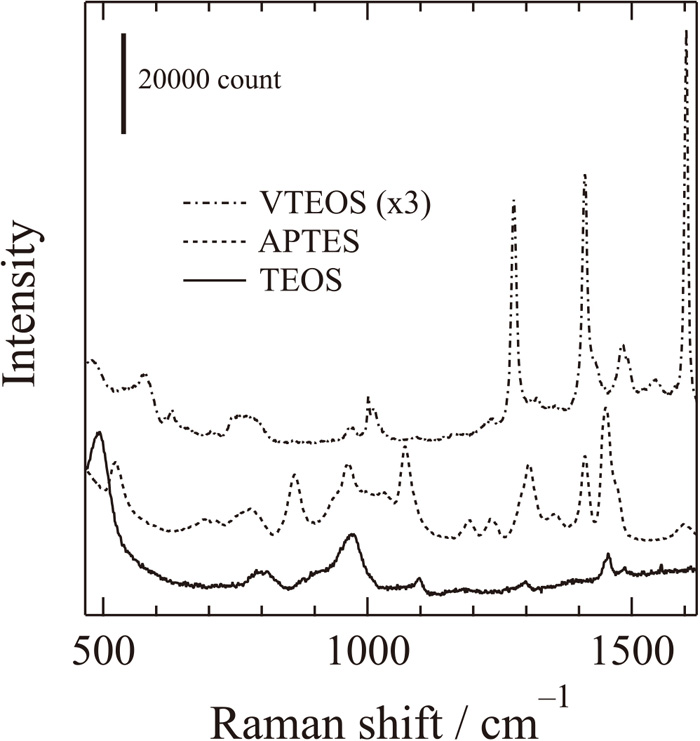
Photolithography with a positive-type photoresist gave a circle-shaped pattern in which there was bare steel surface. However, the resist coating showed poor adhesion to the steel surface and peeled after immersion and cathodic polarization in the aqueous solution, suggesting that the photoresist was an insufficient coating for the microelectrode fabrication. In order to improve the adhesion of the coating, an inner layer of silica was introduced by a sol-gel method before coating of the photoresist. It was expected that the photoresist coating and silica layer would provide patterning and insulation, respectively, for the electrode. Three silane coupling precursors, TEOS, VTEOS and APTES, were selected for the following reasons. TEOS is a typical silane coupling agent that provides silica composed of simple inorganic structure and is expected to provide good adhesion to the steel substrate by condensation reaction and interaction with hydroxyl groups of the substrate surface. VTEOS provides a vinyl group structure in silica. The flexible structure of an inorganic-organic composite is expected to provide hydrophobicity and high durability. APTES is a silane coupling agent in which amino groups show a strong interaction with hydroxyl groups of the substrate. It is expected that the silica derived from APTES would have strong adhesion to the photoresist, which is mainly composed of novolac resin: phenol-formaldehyde resin with a formaldehyde. Figure 1 shows Raman spectra of the layers derived from TEOS, APTES, and VTEOS. In the case of the layer of TEOS, the bands observed at 492, 800 and 971 cm–1 corresponded to HO–SiO3 breathing,8,9) SiO4 asymmetric stretching,10) and Si–OH stretching,9) respectively. Although these bands were also observed in the case of the layers of APTES and VTEOS, bands at 1045 and 1600 cm–1 corresponding to C–N skeletal stretching and -NH2 scissoring, respectively,11) were observed in the layer of APTES. Bands at 633 cm–1 corresponding to in-phase stretching of C–SiO3 and at 1276, 1412, and 1603 cm–1 corresponding to -CH= rocking, CH2= bending, and C=C stretching of vinyl groups12) were observed in the case of VTEOS. The appearance of relatively broad peaks from Si–O bonds indicates the formation of an amorphous silica layer from these precursors. In the separate experiments, the crystallinity of silica was increased with the oxidation of bare steel surface by increasing the heating temperature after the coating. In this study, however, the temperature was kept at a maximum of 383 K so as not to oxidize the steel surface by excess heating.
Although the RIE process was necessary for removing any silica layer at the pattern, a micro-circle pattern was successfully fabricated. Optical micrographs of iron surfaces in Figs. 2(a)–2(c) show the patterning of a circle shape by photolithography with coating of the silica inner layer after removal of the photoresist by washing in acetone. The structural colors of pale green, yellow, and pale red originate from silica layers derived from sol-gel coatings of TEOS (Fig. 2(a)), APTES (Fig. 2(b)), and VTEOS (Fig. 2(c)), respectively, as precursors. The structural colors of pale green and pale red originate from silica layers derived from sol-gel coatings of TEOS and VTEOS, respectively, as precursors, whereas the yellow color of APTES was derived from the photoresist that remained on the outermost silica layer because of strong adhesion due to amide bonding. The thicknesses of layers measured by CLSM were 0.30, 0.99, and 0.60 μm, respectively. On all surfaces, the formation of a circle exposing the iron surface can be clearly seen. The diameter of the circle is about 40 μm, though the diameter was dependent on the coating and sputtering conditions of the silica layer as well as the lighting condition. In the separate treatments, we found that a circular shape with a minimum diameter of 6 μm was successfully formed. The local iron surfaces shown in Figs. 2(a)–2(c) and iron surface of a macroelectrode were immersed in 0.05 M H2SO4 and potentio-dynamically polarized in the cathodic direction at a potential sweep rate of 5 mV s–1 (Fig. 3). Silica-coated surfaces with a circle-shaped pattern showed similar OCPs or slightly positive than OCP around –0.3 VSHE, while the OCP of an iron macroelectrode, which was fabricated by removal of the photoresist from the whole iron surface, was about –0.22 VSHE. The similarity of OCP suggests that the surface with a micro-circle pattern works as a microdisk electrode. However, it was found that the presence of a silica layer affects cathodic current density at the same polarization potential, and TEOS showed the smallest value in all of the silica layers. Figures 2(d)–2(f) show optical micrographs of iron surfaces with a circle-shaped pattern after cathodic polarization of the iron surfaces shown in Fig. 3. The microelectrode surfaces, namely the circle-shaped surfaces, turned not to shining compared with those before the polarization. Edge parts of the silica layer facing the microelectrode surface showed a different morphology from that of the silica surface far from the microelectrode depending on the silica precursor. The difference after cathodic polarization seems to correspond to the excess current density during the polarization. The silica layer derived from TEOS (Fig. 2(d)) showed less difference at the edges and the smallest cathodic current density, indicating that the silica layer from TEOS has the largest resistance and the strongest adhesion among the silica layers and is the most preferable silica layer as an insulating material for the electrode fabrication. Although the reason for the adhesion of silica layers from APTES (Fig. 2(e)) and VTEOS (Fig. 2(f)) being inferior to the silica layer from TEOS is not clear, the density of the inorganic structure seems to be important for not only preventing the penetration of water and oxygen molecules into the silica/substrate interface but also providing strong interaction such as metalloxane bonding at the interface especially at edge parts facing to the microelectrode surface.
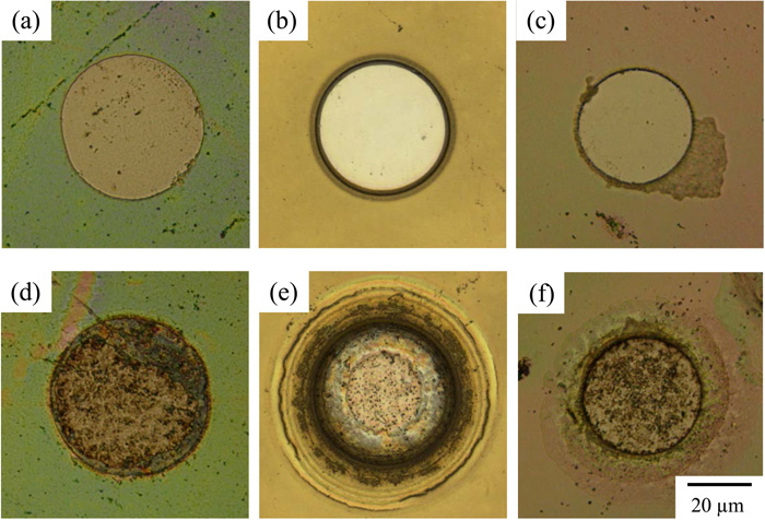
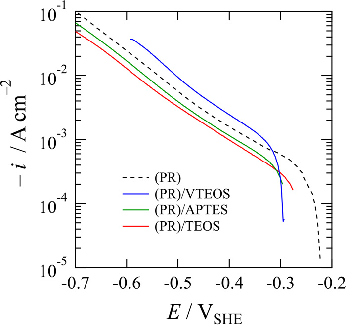
Figure 4 shows Bode line plots of an iron surface covered with a silica layer from TEOS and photoresist without a microelectrode pattern when EIS was carried out after immersion in 0.05 M H2SO4. Just after immersion, phases were almost –90° in the whole frequency region, suggesting that the system corresponds to an equivalent circuit of Rs-Cf, where Rs is the solution resistance and Cf is the film capacitance, and Rs and Cf connect in series. However, phases at low frequencies decreased gradually, suggesting that defects formed and grew in the film, and the system changed to a circuit corresponding to Rs-(RdCf), where Rd is the resistance due to defects in the film, and Rd and Cf connect in parallel.
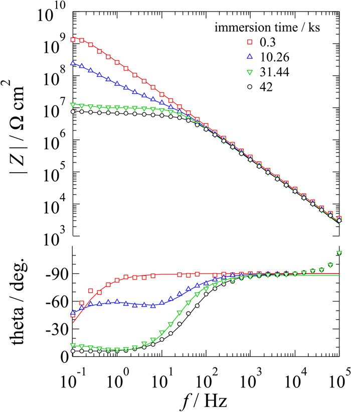
Figure 5 shows time variations of impedance at 0.1 Hz of iron electrodes covered with a photoresist, covered with a silica layer from TEOS and a photoresist, and covered with a silica layer from TEOS and TEOS/GPTMS (8 to 2 in volume) and a photoresist. The photoresist coating itself had high impedance, more than 109 Ω cm2, just after immersion. However, the impedance decreased exponentially with immersion time due to the penetration of water molecules in the film defects. On the other hand, the photoresist with an inner silica layer maintained a relatively high impedance of about 109 Ω cm2 for 1.5×10⁴ s and then the impedance rapidly decreased. It is thought that the silica layer from TEOS combined with the photoresist coating is effective for controlling the formation and growth of film defects and for sustaining the coating resistance as an electrode-fabricating insulator for 1.5×10⁴ s. It is also thought that the decrease in impedance after 1.5×10⁴ s was due to the degradation of the coating/layer interface and penetration of water molecules through defects and pinholes of the inner layer, since the photoresist was easily peeled off from the silica layer from TEOS after the immersion for 2.5×10⁴ s by scratching with a toothpick. Therefore, the coating structure is still imperfect and is not suitable for long immersion of more than 1.5×10⁴ s, which is frequently necessary for a hydrogen permeation test. The photoresist used in this study is mainly composed of novolac resin, which is a phenol-formaldehyde resin with a formaldehyde. It is thought that an imperfect interaction between TEOS and novolac resin provides the weak adhesion between these layers and allows penetration of water molecules between the layers and in the silica layer during long immersion in the electrolyte solution. On the other hand, GPTMS is a silane coupling agent composed of epoxy groups that are etherified with hydroxyl groups of novolac resin,13,14) and the sol-gel films derived from TEOS and GPTMS showed a relatively high impedance because of their flexible structure.15) It is expected that the silica layer derived from sol-gel containing GPTMS shows strong adhesion to the photoresist and high resistance for water penetration. In order to improve the durability of the photoresist with an inner silica layer, a precursor composed of TEOS containing 20 vol% GPTMS16) was coated on a silica layer from pure TEOS and then the photoresist was coated on the composite silica layer surface. It was found that the photoresist with the composite inner layer had excellent durability and showed large impedance of more than 109 Ω cm2 for 4×10⁵ s, and it was not peeled off when the surface was scratched by a toothpick after the immersion for 4×10⁵ s. It is obvious that the photoresist with the composite silica inner layer is the most suitable as an insulating material for microelectrode fabrication on the iron surface studied here. In the following experiments, this composite silica layer as an inner layer of the photoresist coating was used for fabrication of all of the microelectrode by photolithography, and electrochemical measurements were carried out with the microelectrode of iron or steel which was covered with an inner silica layer obtained from TEOS, an outer composite silica layer obtained from TEOS and GPTMS, and photoresist. The total thickness of the coating measured by CLSM was about 4 μm.
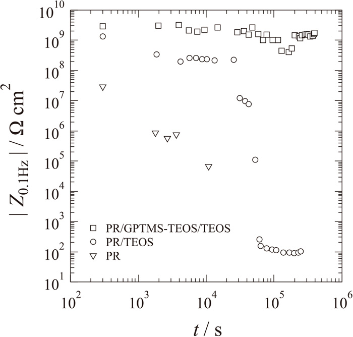
Figure 6(a) shows anodic polarization curves of an iron macro electrode and an iron microelectrode with a diameter of 80 μm in 0.05 M H2SO4. Although OCP of the microelectrode and the initial relation in the potential region until –0.25 VSHE are the same as those measured using the macroelectrode, the microelectrode tended to have a larger current density in an active state and to be in a passive state from 0.4 VSHE. The former difference is due to acceleration of the mass-transport process of dissolved species from the electrode surface in a radial direction of the microelectrode. It is obvious that a semispherical concave is formed at the microelectrode surface after the polarization as shown in Figs. 6(b) and 6(c). The volume of the concave measured by CLSM was 6.09×104 μm3, which is in good agreement with the volume of Fe dissolved as ferrous species (6.09×104 μm3) calculated from an electric charge of 1.66×10⁻³ C consumed in the active region of Fig. 6(a). In any case, the maximum depth of the concave formed during anodic polarization was 17.1 μm, which might be a non-negligible size to discuss the electrochemical behavior of the microelectrode with a diameter of 80 μm. Application of the microelectrode to anodic dissolution seems to be limited to measurement that consumes a very small electric charge. In the initial stage of the active state in Fig. 6(a), however, a linear relationship with a slope of 40 mV, which is the Tafel slope in the so-called Bockris mechanism of iron dissolution,17) is clearly obtained, suggesting that the microelectrode is an effective tool for studying the electrode reaction mechanism.
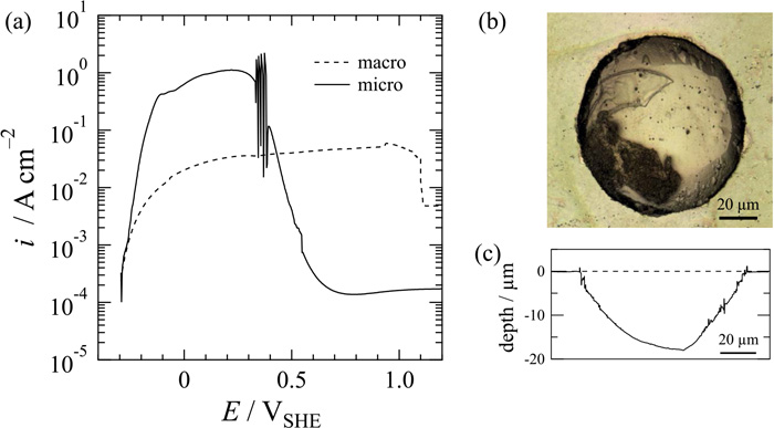
Figure 7(a) shows cathodic polarization curves of iron microelectrodes with a diameter of 50 μm in deaerated 0.05 M H2SO4 when the microelectrodes were fabricated on single grains with relatively lower indices’ planes of {111}, {100}, and {110} as shown in the EBSD inverse pole figure maps in Figs. 7(b)–7(d). OCPs are about –0.27 VSHE and OCP of the {111} plane is more negative than those of {100} and {110} planes by only 20 mV. Although the difference in OCP of the index plane seems to be slightly small, the order of OCPs is in agreement with that reported previously using handmade microelectrodes.18) It is thought that the small difference is due to the formation of oxide on the microelectrode surface after the RIE removal of the silica layer. On the other hand, cathodic current density of three indices’ planes increased with increase in overpotential in the cathodic direction. When the Tafel slope of –112 mV, independent of the plane orientation,18) is adopted in a small overpotential region until –0.35 VSHE, exchange current densities of {100}, {111}, and {101} planes calculated using extrapolate lines with the slope are 8.1×10⁻⁷, 4.8×10⁻⁷, and 4.5×10⁻⁷ A cm–2, respectively. Although the calculated values are slightly larger than the previous values,18) the dependence of the value on the plane orientation is in good agreement with that reported previously, indicating that the rate of HER in a charge transfer controlling region is strongly related to the microstructure and/or electronic state of the iron electrode surface. In the large overpotential region below –0.35 VSHE, on the other hand, cathodic current density at the same potential increased in the order of {101} < {100} < {111} planes: for example, 2.60, 2.94, and 4.40 mA cm–2 for {101}, {100}, and {111} planes, respectively, at –0.50 VSHE. This is different from the above but the same as the order of surface roughness (1.21, 1.70, and 2.94 for {101}, {100}, and {111} planes, respectively).19) The rate of HER in this region might be dependent on the metallographic structure of the electrode surface. However, the current density of any index plane does not show a limited and stable value even in the large overpotential region and it increases exponentially with increase in overpotential with a slope of –200 mV. The variation of the slope from –112 mV means the change in processes of HER due to the large overpotential, in which a coverage of adsorbed hydrogen on the surface is close to unity and the metallographic structure of the surface allows additional processes for HER. Furthermore, the rate of HER is also partially determined by mass-transport of hydrogen molecules generated from the electrode. It is thought that the slope might vary with changes in the microelectrode diameter, coating thickness, and solution acidity.
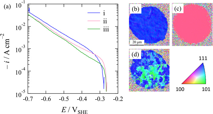
Figure 8(a) shows an optical micrograph of the SCM435 steel surface after etching with nital, which was 10 vol.% HNO3 ethanol. It was thought from the heat treatment condition that the whole surface was composed of the matrix of tempered martensite and bainite. However, relatively large grains with a diameter of 500 μm were seen in the matrix. Since Vickers hardness of the matrix and grain were 313 Hv0.5 and 760 Hv0.5, respectively, it is thought that the heat treatment was not appropriate and that the grains are not tempered martensite containing a large amount of carbon compared with the matrix. Figures 8(b)–8(d) show optical micrographs of SCM435 steel microelectrodes prepared by the photolithography developed in this study. The diameters of microelectrodes, indicating white circles in Figs. 8(b)–8(d), composed of the matrix of tempered martensite/bainite, grains of martensite, and a dual structure of tempered martensite/bainite and martensite are almost all 40 μm.
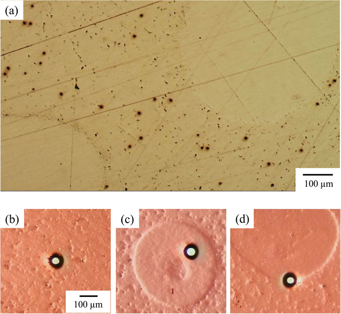
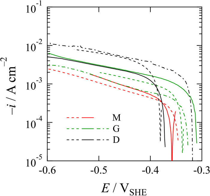
Figure 9 shows cathodic polarization curves of the SCM435 steel microelectrodes shown in Figs. 8(b)–8(d) in deaerated 0.05 M Na2SO4 with pH adjusted to 3.0 by addition of H2SO4. The measurements were carried out two or three times with independent microelectrodes of matrix of tempered martensite/bainite, grain of martensite, and dual structure of tempered martensite/bainite and martensite fabricated from a piece of SCM435 steel specimen. The values of OCP are between –0.38 and –0.30 VSHE, which are negative compared with that of iron (ca. –0.27 VSHE), indicating that the anodic iron dissolution reaction is active or that the cathodic HER is inactive. The negative shift of OCP of the SCM435 steel seems to be due to the presence of additional elements and/or differences in surface structure and mechanical property. However, they should complementally affect the anodic and cathodic reactions, and it is difficult to specify the main factor determining reaction activities from the comparison between separate materials. Although there is large scattering of values, on the other hand, the grain of martensite shows a more positive OCP than that of the matrix of tempered martensite/bainite. It is interesting that the dual structure composed of tempered martensite/bainite and martensite shows the same value as the OCP of either structure. At one potential such as –0.50 VSHE, on the other hand, the cathodic current density of the matrix of tempered martensite/bainite is smaller than that of the grain of martensite, and these cathodic current densities of single structures are smaller than that of the dual structure. It is apparent that the HER activity strongly depends on the metallographic structure and that a harder structure has a higher activity for HER. Defects and dislocations that characterize the structure and its hardness also characterize a structure/solution interface and seem to determine the HER activity. Although the reason of high HER activity due to the hard structure is not clear, the finding is supported by the previous studies that the exchange current density for HER increased with increase in hardness of material.20) Since the hydrogen diffusion coefficient decreases with increase in hardness of material,20,21) it is thought that a harder structure allows a larger reactivity for hydrogen permeation.
The photolithographic fabrication of the steel microelectrode discussed here resulted in a coating with a thickness of about 4 μm. The durability of the insulating material on the microelectrode was confirmed for at least 3×10⁵ s. Therefore, the microelectrode has successfully been applied to hydrogen permeation measurements with solution fluctuation22) and potential fluctuation23) with the DS cell. After the statistical examination to check the reproducibility, in the near future, we will present results of the hydrogen permeation measurements with the photolithographically fabricated microelectrode on the steel and the dependence of hydrogen permeation on the metallographic structure of the material.
4. Conclusions
Microelectrodes of iron and steel were fabricated by photolithography using a positive-type photoresist. The photoresist coating which was essential for the formation of a circle-shaped pattern with a diameter of several tens of micrometers on iron material showed rapid decreases of adhesion and impedance during immersion in H2SO4. However, a silica layer derived from TEOS was effective for fabricating high impedance coating on the iron substrate as an electrode insulating material. Moreover, the addition of an outer layer of silica from a mixture of TEOS and GPTMS resulted in improvements in adhesion of the silica layer from TEOS and photoresist of the coating and durability of the coating for 4×10⁵ s in H2SO4. Potentio-dynamic polarization of an iron microelectrode with a diameter of several tens of micrometers in the anodic and cathodic directions in H2SO4 revealed that the iron dissolution reaction became clear due to promotion of the mass-transport process from the electrode surface and that the HER was dependent on the plane orientation, respectively. The HER on SMC435 steel was also strongly dependent on the surface microstructure. It was thought that the dependence of HER on the surface microstructure of iron and steel substrates would affect the hydrogen permeation behavior of the substrate.
Acknowledgement
The authors thank Prof. Mitsuo Kimura, The University of Tokyo, for the kind discussion about the microstructure of steel. This work was conducted at Hokkaido University and supported by the study group of “Corrosion-induced Hydrogen Absorption to Steels” in Iron and Steel Institute of Japan and “Nanotechnology Platform” Program of Ministry of Education, Culture, Sports, Science and Technology (MEXT), Japan.
References
- 1) M. Sakairi: ISIJ Int., 56 (2016), 377.
- 2) K. Fushimi, M. Jin, Y. Kitagawa, T. Nakanishi and Y. Hasegawa: ISIJ Int., 56 (2016), 431.
- 3) S. Kudelka, A. Michaelis and J. W. Schultze: Ber. Bunsenges. Phys. Chem., 99 (1995), 1020.
- 4) M. Schweinsberg, S. Kudelka, A. Michaelis and J. W. Schultze: Mater. Corros., 49 (1998), 161.
- 5) Y. Jin, Z. Lai, P. Bi, S. Yan, L. Wen, Y. Wang, J. Pan and C. Leygraf: Electrochem. Commun., 87 (2018), 53.
- 6) N. Ishii, Y. Kitagawa, Y. Hasegawa and K. Fushimi: Proc. JSCE Mater. Eng. 2019, Japan Society of Corrosion Engineering, Tokyo, (2019), 131, CD-ROM (in Japanese).
- 7) A. B. Wojcik and L. C. Klein: J. Sol-Gel Sci. Technol., 4 (1995), 57.
- 8) C. Mulder and A. Damen: J. Non-Cryst. Solids, 93 (1987), 387.
- 9) K. Matsui, H. Satoh and M. Kyoto: J. Ceram. Soc. Jpn., 106 (1998), 528.
- 10) M. C. Matos, L. M. Ilharco and R. M. Almeida: J. Non-Cryst. Solids, 147–148 (1992), 232.
- 11) I. Shimizu, H. Okabayashi, K. Taga and C. J. O’Connor: Colloid Polym. Sci., 275 (1997), 555.
- 12) K. Gigant, U. Posset, G. Schottner, L. Baia, W. Kiefer and J. Popp: J. Sol-Gel Sci. Technol., 26 (2003), 369.
- 13) C.-L. Chiang, C.-C. M. Ma, D.-L. Wu and H.-C. Kuan: J. Polym. Sci., Part A: Polym. Chem., 41 (2003), 905.
- 14) M. R. Acocella, C. Esposito Corcione, A. Giuri, M. Maggio, A. Maffezzoli and G. Guerra: RSC Adv., 6 (2016), 23858.
- 15) J. Hu, Q. Li, X. Zhong, L. Zhang and B. Chen: Prog. Org. Coat., 66 (2009), 199.
- 16) L. M. Rueda, C. Nieves, C. A. Hernández Barrios, A. E. Coy and F. Viejo: J. Phys. Conf. Ser., 687 (2016), 012013.
- 17) J. O’M. Bockris and A. K. N. Reddy: Modern Electrochemistry, Vol. 2, Plenum Press, New York, (1973), 991.
- 18) K. Fushimi, K. Miyamoto and H. Konno: Electrochim. Acta, 55 (2010), 7322.
- 19) P. Błoński and A. Kiejna: Surf. Sci., 601 (2007), 123.
- 20) T. Haruna and Y. Nii: ISIJ Int., 56 (2016), 392.
- 21) H. Hagi and Y. Hayashi: J. Jpn. Inst. Met., 51 (1987), 24.
- 22) Y. Yamamoto, Y. Kitagawa, T. Nakanishi, Y. Hasegawa and K. Fushimi: ISIJ Int., 56 (2016), 472.
- 23) Y. Yamamoto, Y. Kitagawa, Y. Hasegawa and K. Fushimi: J. Electrochem. Soc., 165 (2018), C900.