Abstract
We have succeeded in improving the gain of the base quantum cascade laser (QCL) through
experiments and device simulations using the nonequilibrium Green’s function (NEGF)
method, and we investigate the factor that increases the gain by reducing the thickness of
the barrier by 10%. Specifically, we analyzed the minibands (Wannier–Stark states),
density of states (DOS), and electron density that contribute to the emission. The results
show that the gain enhancement is due to the increase in the electron density of the
quantum wells in the active region and the increase in the oscillator strength between the
minibands that contribute to the emission. Quantum mechanical calculation like the NEGF
method is very effective for mesoscopic systems such as the active layer of QCL.
1 INTRODUCTION
Quantum cascade laser (QCL) is a semiconductor laser that emits mid- and far-infrared rays.
The active layer of QCL is a mesoscopic system consisting of multiple layers of
InxAl(1-x)As/InyGa(1-y)As. Its oscillation
wavelength can be controlled by changing the material and thickness of the layer [1]. By making the active layer multistaged, it is possible
to reuse electrons that had already contributed to the laser emission and to achieve high
quantum efficiency and high output.
Currently, the QCL has been applied to various fields such as semiconductor processes,
optical frequency combs, combustion diagnosis of engines, the discovery of drugs and
explosives, and life science [2,3,4,5,6,7]. Since its wavelength is in the infrared region, the application to trace gas
analysis and remote gas detection is particularly noticeable [8, 9]. To achieve this, a QCL with a
wavelength suitable for such measurements is required. In addition, with such trace
substance detection and remote gas detection, higher sensitivity is expected by increasing
the output. Since the amount of laser absorption is measured in the detection of trace
substances, the laser must propagate along a long optical path. To develop a laser with such
a high output and a wavelength suitable for measurement, it is effective to use a simulation
method that can predict the oscillation wavelength and gain.
In the simulation, the Schrödinger equation is first solved to calculate the eigenvalues
and eigenfunctions, that is, the energies and the wavefunctions. The laser light intensity
is then calculated from the upper and lower level lifetimes and the transition probabilities
between the upper and lower levels. To reproduce them and calculate the oscillation
wavelength and gain with high precision in the simulation, how the electron dynamics are
calculated is important. QCL skillfully applies the electron dynamics such as the optical
transition of electrons between subbands in the conduction band of the active layer and
electron transport to the next active layer by the tunnel effect in the miniband of the
injector region. Calculation methods of such electron dynamics are, for example, the rate
equation [10], the MC method [11], and the nonequilibrium Green’s function (NEGF) method [12,13,14]. This work is based on the NEGF method.
In the rate equation and MC approaches, the electron density distribution and the
transition of electrons from the upper level to the lower level can only be calculated
semi-classically [15]. On the other hand, in the
calculation using the NEGF, they can be calculated quantum mechanically [16,17,18,19,20]. Furthermore, by determining the self-energy of
electron scattering, we can easily add the effect of electron scattering on the electron
distribution. Not only can the gain be calculated accurately, it is also possible to reflect
the effects of operating temperature and strain.
We ran the simulations that incorporate the NEGF method for the calculation of electron
dynamics in QCLs [21,22,23,24]. In previous work [25], the active
layers of the QCLs were designed to increase the gain using a simulator, and it was shown
that the output could be improved by thinning the barrier of the active region. As a result
of evaluating a QCL of this structure, the EL emission intensity was found to be increased
1.4-fold compared with the QCL of the base structure. In this work, to check the correctness
of input and output, the current–voltage (IV) characteristic was also verified. The
calculated values of the IV characteristic well reproduced the tendency of the measured
values. Furthermore, the calculated values of the oscillation wavelength by the NEGF method
were in good agreement with the measured values. The wavelengths were explained from the
energy difference of the minibands (Wannier–Stark states), which mainly contributes to the
emission. We also analyzed the origin of the gain from the density of states (DOS), electron
density, and oscillator strength. The NEGF calculations are found to be very useful in
computational chemistry for the mesoscopic system, such as the active layer of QCL.
The novelty of this work is that the cause of the improvement was analyzed in detail from
the minibands (the eigenstates of the Schrödinger equation without accounting for Poisson
equation), the density of states, electron density, and oscillator strength.
2 THEORETICAL METHODS
2.1 Composition simulator
The nextnano.NEGF software (nextnano GmbH) [26]
was used for calculating the optical gains, IV characteristics, and the oscillation
wavelengths of QCLs [21,22,23,24].
Figure 1 shows the calculation flow in the
simulation. The simulator uses field-periodic boundary conditions. In this way, the
simulation accounts for an infinite periodic structure, with a periodic electric field.
First, the single-band effective mass Schrödinger equation is solved in real space. As a
second step, the scattering coupling terms are calculated for each of the mechanisms
(longitudinal polar-optical phonons scattering, charged impurities scattering, interface
roughness scattering, alloy disorder scattering, and electron-electron scattering).
Acoustic phonons scattering is not in general efficient and is neglected in this work.
Assuming that the unperturbed Hamiltonian is
H
^
0
(^ indicates that it is an operator) and the perturbation
term for the electron scattering is
H
^
scatt
, the Hamiltonian
H
^
in the Schrödinger equation is expressed by
|
H
^
=
H
^
0
+
H
^
scatt
,
| (1) |
where
H
^
0
is an exactly solvable part.
H
^
scatt
contains impurity, phonon, or electron-electron scattering
matrix elements and is solved perturbatively.
Then, the main part of the calculation consists of the self-consistent NEGF solver. We
start to find an initial guess of the lesser Green’s function
G< by solving the Schrödinger equation, where
G< is also called the correlation function. Next, the
Poisson equation is solved to find the mean-field electrostatic potential, and the
retarded self-energy ΣR and the lesser self-energy
Σ< are calculated. ΣR and
Σ< can be expressed by [27]
|
Σ
R
=
G
R
D
R
+
G
R
D
<
+
G
<
D
R
,
| (2) |
where
DR and
D< are the sums of retarded and lesser Green’s
functions of the environment.
The retarded Green’s function GR is derived using the Dyson
equation expressed by
|
G
R
=
1
E
−
H
^
0
−
Σ
R
.
| (4) |
Here, E is the energy. Using the Keldysh equation shown as equation (5),
we obtain the lesser Green’s function G<,
where
GA is an
advanced Green’s function.
GA and
GR are Hermitian conjugates, i.e.,
GA = [
GR]
†.
G< obtained from equation (5) is compared with the
initial
G<, and the calculation is repeated until it
converges to the set threshold. That is,
G< is obtained by
a self-consistent method. The electron density matrix is obtained from
G<. The current density is directly calculated, as well
as the electron density. Based on the electron density matrix, the optical gain and the
current of the QCL are calculated. The energy-resolved density matrix
ρ
(
E
)
is
|
ρ
(
E
)
=
−
i
2
π
∫
d
E
G
<
(
E
)
.
| (6) |
The electron density is given by the diagonal term of
ρ(E). The spectral function, i.e., DOS, is the
imaginary part of the retarded Green’s function GR.
By using the NEGF method, both quantum transport effects (i.e., coherent transport
effects such as resonant tunneling) and scattering mechanisms can be accounted for. This
makes it suitable for QCL simulations [28,29,30].
From a series of calculations, the relationship between the energy (wavelength) and the
gain is calculated. The oscillation wavelength of the laser is determined as the
wavelength that maximizes the gain. By using the NEGF method, it is possible to perform
the calculation while taking into consideration of the effects of the strain and electron
scattering on the crystal lattice corresponding to the operating temperature of the
QCL.
2.2 Optical gain
This subsection is based on Grange’s commentary [31]. The optical gain is obtained as follows [32,33,34]. The gain self-consistent calculation calculates the linear response to the
input AC electromagnetic field. It is performed for each possible frequency (photon
energy) within the gain calculation. In this case, the perturbation due to an AC electric
field along z(coordinate in growth direction) is considered. The
perturbating Hamiltonian is:
|
H
^
A
C
=
e
z
δ
F
e
−
i
ω
t
| (7) |
in the Lorenz gauge, where
e is the elementary charge,
F is the electric field,
ω
is the angular frequency, and
t is the
time. The response Green’s function
δ
G
<
(
ω
,
E
)
is calculated within linear response theory. According to
Wacker [
32], the Green’s function linear responses
are:
|
δ
G
R
(
ω
,
E
)
=
G
R
(
E
+
h
ω
2
π
)
(
H
^
A
C
+
δ
Σ
R
(
ω
,
E
)
)
G
R
(
E
)
,
| (8) |
and
|
δ
G
<
(
ω
,
E
)
=
G
R
(
E
+
h
ω
2
π
)
H
^
A
C
G
<
(
E
)
+
G
<
(
E
+
h
ω
2
π
)
H
^
A
C
G
A
(
E
)
+
G
R
(
E
+
h
ω
2
π
)
δ
Σ
R
(
ω
,
E
)
G
<
(
E
)
+
G
R
(
E
+
h
ω
2
π
)
δ
Σ
<
(
ω
,
E
)
G
A
(
E
)
+
G
<
(
E
+
h
ω
2
π
)
δ
Σ
A
(
ω
,
E
)
G
A
(
E
)
.
| (9) |
In the self-consistent gain calculation, the 3 last terms in equation (9) are accounted
for. Indeed, to account for them, the self-energies
δ
Σ
(
ω
,
E
)
need to be calculated from
δ
G
<
(
ω
,
E
)
, requiring a self-consistent loop.
From this Green’s function response, the AC conductivity is calculated as
|
σ
(
ω
)
=
δ
j
(
ω
)
δ
F
.
| (10) |
Here,
|
δ
j
(
ω
)
=
T
r
(
G
<
J
)
,
| (11) |
where
J is the current
operator.
The bulk dielectric constant is assumed to be given by the Lyddane-Sachs-Teller relation
[35]:
|
ϵ
r
b
u
l
k
(
ω
)
=
ϵ
∞
+
(
ϵ
∞
−
ϵ
s
t
a
t
i
c
)
ω
T
O
ω
2
−
ω
T
O
2
,
| (12) |
where
ϵ
∞
is the dielectric constant at very high frequencies,
ϵ
s
t
a
t
i
c
is the static dielectric constant, and
ω
T
O
is the transverse optical phonon frequency. In the
self-consistent gain calculation, the quantity which is calculated is the AC conductivity
σ
(
ω
)
. The complex dielectric constant is then:
|
ϵ
r
(
ω
)
=
ϵ
r
b
u
l
k
(
ω
)
−
i
σ
(
ω
)
ω
ϵ
0
,
| (13) |
where
ϵ
0
is the vacuum permittivity. Finally, the gain
is
|
g
(
ω
)
=
−
R
e
(
σ
(
ω
)
)
ϵ
r
(
ω
)
.
| (14) |
When the oscillator strength between the subbands contributing to the photoemission is
stronger, the gain is also higher. At the same time, the gain is higher when the
population inversion is achieved. Thus, increasing the gain requires two contradictory
conditions.
3 RESULTS AND DISCUSSION
3.1 The active layer of QCL
To obtain experimental values of electroluminescence (EL) emission intensity, IV
characteristics, and oscillation wavelengths, a prototype was made using the structure
reported by Evans et al. [36], and these physical
properties were measured.
The materials of our prototype are Ga0.331In0.669As for the wells
and Al0.638In0.362As for the barriers. In this structure, one period
of the active layer consists of 22 layers, the injection region is from the 1st to 14th
layers, and the active region is from the 15th to 22nd layers. The injection region is
doped with Si (its concentration is 2.0 × 1016 cm−3). The
thicknesses in nanometers for one period are as follows: 2.8,
1.7, 2.5,
1.8, 2.2,
1.9, 2.1,
2.1, 2.0,
2.1, 1.8,
2.7, 1.8,
3.8, 1.2,
1.3, 4.3, 1.3, 3.8, 1.4, 3.6, 2.2,
where values for the barriers are in bold and those for wells are in normal font. The
underlined thicknesses represent the doped layers. This structure is denoted as APL91. The
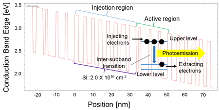
device structure has a ridge width of 15 µm and a length of 4 mm. Figure 2 shows the conduction band of APL91. Electrons are injected
from the injection region into the upper subband of the active region, and they drop to
the lower subband through the intersubband transition. Photoemission occurs at that
time.
We attempted to design a high-power active layer for QCLs using the NEGF method [25]. The design was based on the structure shown in
Figure 2 [35]. The thicknesses of barriers in the active region are changed to achieve
high gain. Many cases were calculated while adjusting parameters, such as net strain,
calculation range, and convergence condition.
Simulations with various parameters were performed based on physical considerations. The
structure with the noticeable change in gain was that in which the thicknesses of the
barriers in the active region were varied. The calculated gains of this design are shown
in Figure 3. When the barriers in the active
region were reduced, the gain increased, and a maximum gain that is 1.28 times that in
APL91 is observed. On the other hand, in the structures in which the thicknesses of
barriers are increased, the gains are lower than those in APL91.

Based on calculation results, for measuring EL, we fabricated devices with 10% thinner
barriers in the active region (−10% device) and APL91. The device length is 2 mm and the
ridge width is 100 μm. The device is soldered onto a Cu/W mount. We used the Nicolet8700
Thermo Scientific to measure the EL spectrum. The emitted light is focused by a mirror,
and the EL intensity is measured by MCT (HgCdTe) detector. The prototypes were operated at
a frequency of 100 kHz, a pulse width of 300 nm (duty 3%), and 77 K.
Figure 4 shows the EL spectra of the
prototypes. The horizontal axis represents wavelength and the vertical axis represents EL
emission intensity. Good emission is observed in the −10% device. The wavelengths of APL91
and the −10% device are 4.53 μm and 4.77 μm, respectively. The EL emission intensities are
1.50 and 2.05, respectively. In other words, the EL emission intensity of the −10% device
increased 1.37 times that of APL91. Although slightly larger than the value obtained in
the simulation, a strong EL emission intensity was achieved as calculated.
The simulator needs to be able to reproduce not only the gain but also the electrical
characteristic of the device with high accuracy. IV characteristic is a typical electrical
characteristic. To verify the accuracy of the simulator, we focused on the IV
characteristic and compared the simulated and experimental values. The prototype in
Subsect. 3.1 was used again to obtain experimental values of the IV characteristic.
We measured the peak current and voltage, but the simulator outputs the relationship
between current density and voltage, so the current was converted to current density from
the ridge width and device length for comparison. Figure 5 shows the simulation and experimental results of the IV characteristic.
Although the shape of the curves is slightly different, values are relatively close, and
both of them show an increase in voltage as the current density increases. In the
simulation, it is assumed that all the input voltage is applied to the active layer.
Therefore, although there is a slight difference between the measured and calculated
values, we judged that this level of difference was sufficient to achieve the purpose of
this work.
3.3 Analysis of wavelength and gain
High outputs can be expected from the structure with thin barriers in the active region,
but if the structure is markedly changed, fabricating the prototype becomes difficult
because the net strain increases as the thickness decrease. Therefore, the wavelengths
were calculated for a structure with a 10% thinner barrier (−10% structure) and a
structure with a 10% thicker barrier (+10% structure).
Figure 6 shows the minibands (Wannier-Stark
states) of APL91 at a voltage of 400 mV per period and a temperature of 300 K. The
Wannier-Stark states correspond to the eigenstates of the Schrödinger equation without
accounting for Poisson equation (i.e., electrostatic mean-field). All three structures
consist of 14 minibands. The minibands that contribute to the emission and their energy
differences are shown in Figure 7. Which
miniband mainly contributes to the emission was determined from the oscillator strength.
The main contribution to the emission was level 4 to level 6 transition. Let
Δemi be the energy difference between level 4 and level 6. The energy
difference Δemi of APL91 is 264.2 meV, which is 4.697 μm when converted to
wavelength. Δemi values of the −10% structure and +10% structure are 251.5 meV
(4.934 μm) and 272.0 meV (4.562 μm), respectively. The wavelength for the −10% structure
is longer because Δemi of the −10% structure is smaller than that of APL91.
Similarly, Δemi of the +10% structure is larger than that of APL91, so the
wavelength of the +10% structure is shorter.

Figure 8 shows the calculated wavelengths.
Since the experimental wavelength of APL91 is 4.708 μm [28], the calculated value is in good agreement with the experimental one. −10%
structure had a slightly longer wavelength than APL91. On the other hand, the wavelength
was shortened in +10% structure. In Figure 4,
the oscillation wavelength of −10% structure is 4.77 μm, which is in good agreement with
the simulation results.

Figure 9 shows DOSs at a voltage of 400 mV per
period and a temperature of 300 K for APL91, −10% structure, and +10% structure. The DOS
of a system is a physical quantity describing the number of states for each energy level
that can be occupied by the system within a small energy interval. If the DOS is high at
an energy level, it means that many states can occupy that energy level, and if the DOS is
zero, it means that the system cannot occupy that energy level. The product of DOS and
Fermi–Dirac distribution gives the electron density. −10% structure, which shows a higher
gain than APL91, can occupy more states in the active region, whereas +10% structure,
which shows a lower gain than APL91, has fewer states that can be occupied in the active
region.

Electron densities at a voltage of 400 mV per period and a temperature of 300 K are shown
in Figure 10. In the electron density diagram,
the electron density is higher in the well adjacent to the thick barrier of the injection
region. Electrons are injected from this well into the active region. In addition, large
values of electron density are distributed in the upper and lower subbands of the active
region. Strong luminescence is generated as a result of these electron density
distributions. Comparing the electron densities of APL91 and −10% structure, the electron
density of −10% structure is higher in the upper subband of the second well and the lower
subband of the fourth well of the active region. This is most likely contributing to the
higher gain of −10% structure. Both structures achieve the population inversion in the
wells of the active region, so high gains are obtained. The overall electron density
distribution of +10% structure is lower than that of APL91 and −10% structure, especially
in the active region, which contributes to the emission, and this may be the reason for
the low gain of +10% structure.

The populations of minibands of upper and lower levels for APL91 are 0.109 and 0.054,
respectively. On the other hand, the populations of minibands of upper and lower levels of
the −10% device are 0.121 and 0.054, respectively. Both APL91 and the −10% device achieve
population inversion, but the degree of inversion is larger in the −10% device. It is
thought to be the reason why the EL emission intensity of the −10% device increased. In
addition, the oscillator strength between the upper level 4 and lower level 6 represents
the likelihood of inter-subband transition. The unnormalized oscillator strengths of APL91
and the −10% device are 14.7 and 15.7, respectively; the −10% device is stronger. This may
have also contributed to the increased EL intensity.
4 CONCLUSION
As one of the important targets for mesoscopic systems in computational chemistry, we
selected a QCL and calculated the physical properties, i.e., optical gains, the IV
characteristic, and the oscillation wavelengths using the NEGF method. The active layer was
designed to increase the gain. It was shown that the output could be improved by reducing
the barrier thicknesses in the active region. The reasons for the increase in gain were
analyzed using DOS and electron density. DOS and electron density in the active region of
−10% structure are increased compared to APL91, which is the origin of the gain enhancement.
We fabricated QCL devices with the improved structure and the base structure, and evaluated
their output wavelengths and EL emission intensities. As a result, the wavelengths of our
prototypes were found to be in good agreement with the calculated values. The origins of the
wavelength variation were analyzed using energy differences of the minibands
Δemi. Δemi is the smallest in −10% structure, and as a result, the
oscillation wavelength is the longest in −10% structure. DOS and electron density in the
active region, and oscillator strength between level 4 and level 6 are the largest in −10%
structure, resulting in a higher gain.
It was found that NEGF calculations are very useful in analyzing the properties and
validating novel structures of QCL.
ACKNOWLEDGMENTS
This work was supported by Innovative Science and Technology Initiative for Security (Grant
Number JPJ004596), ATLA, Japan.
SUPPLEMENTARY MATERIALS
Material data and adjustments of parameters
REFERENCES
- [1] J. Faist, F. Capasso, D. L.
Sivco, C. Sirtori, A. L. Hutchinson, A. Y. Cho, Science, 264, 553 (1994). ,
doi:10.1126/science.264.5158.553 PMID:17732739
- [2] J. Faist, Quantum Cascade Laser
(Oxford University Press, United Kingdom, 2013).
- [3] A. Hugi, G. Villares, S.
Blaser, H. C. Liu, J. Faist, Nature, 492, 229 (2012). , doi:10.1038/nature11620
PMID:23235876
- [4] J. Faist, G. Villares, G.
Scalari, M. Rösch, C. Bonzon, A. Hugi, et al., Nanophotonics, 5, 272 (2016).
doi:10.1515/nanoph-2016-0015
- [5] J. Ye, S. T. Cundiff,
Femtosecond Optical Frequency Comb: Principle, Operation, and Applications (Springer,
Norwell, MA, 2005).
- [6] A. M. Weiner, Ultrafast Optics
(Wiley, New York, 2009).
- [7] R. F. Curl, F. Capasso, C.
Gmachl, A. A. Kosterev, B. McManus, R. Lewicki, et al., Chem. Phys. Lett., 487, 1 (2010).
doi:10.1016/j.cplett.2009.12.073
- [8] I. F. Howieson, Laser Focus
World, 47, 33 (2011).
- [9] J. B. McManus, M. S.
Zahniser, D. D. Nelson, J. H. Shorter, S. Herndon, E. Wood, et al., Opt. Eng., 49, 111124
(2010). doi:10.1117/1.3498782
- [10] S. L. Lu, L. Schrottke, S.
W. Teitsworth, R. Hey, H. T. Grahn, Phys. Rev. B, 73, 033311 (2006).
doi:10.1103/PhysRevB.73.033311
- [11] R. C. Iotti, F. Rossi, Rep.
Prog. Phys., 68, 2533 (2005). doi:10.1088/0034-4885/68/11/R02
- [12] J. Schwinger, J. Math.
Phys., 2, 407 (1961). doi:10.1063/1.1703727
- [13] L. P. Kadanoff, G. Baym,
Quantum Statistical Mechanics (W. A. Benjamin, Inc., Menlo Park, California,
1962).
- [14] L. V. Keldysh, Sov. Phys.
Jetp-USSR, 20, 1018 (1965).
- [15] C. Jirauschek, T. Kubis,
Appl. Phys. Rev., 1, 011307 (2014). doi:10.1063/1.4863665
- [16] S. Datta, Electronic Transport
in Mesoscopic Systems (Cambridge University Press, New York, 1995)
Chap. 8.
- [17] S. Datta, Quantum Transport:
Atom to Transistor (Cambridge University Press, New York, 2005).
- [18] S. Datta, Superlattices
Microstruct., 28, 253 (2000). doi:10.1006/spmi.2000.0920
- [19] T. Miyoshi, M. Ogawa, H.
Tsuchiya, Nanoerekutoronikusu No Kiso (Nano Electronics) (Baifukan, Tokyo,
2007).
- [20] S. C. Lee, F. Banit, M.
Woerner, A. Wacker, Phys. Rev. B, 73, 245320 (2006).
doi:10.1103/PhysRevB.73.245320
- [21] T. Grange, Physical
Review B 92, 241306–31–5 (2015).
- [22] T. Grange, Appl. Phys.
Lett., 105, 141105 (2014). doi:10.1063/1.4897543
- [23] T. Grange, Phys. Rev. B, 89,
165310 (2014). doi:10.1103/PhysRevB.89.165310
- [24] T. Grange, D. Stark, G.
Scalari, J. Faist, L. Persichetti, L. Di Gaspare, et al., Appl. Phys. Lett., 114, 111102
(2019). doi:10.1063/1.5082172
- [25] S. Takagi, H. Tanimura, T.
Kakuno, R. Hashimoto, K. Kaneko, S. Saito, Proceedings of the 8th International Conference
on Photonics, Optics and Laser Technology, in Valletta, Malta (2020).
- [26] nextnano.NEGF software
can be purchased from the website of nextnano GmbH.
- [27] H. Haug, A.-P. Jauho, Quantum
Kinetics in Transport and Optics of Semiconductors (Springer, Berlin,
1996).
- [28] T. Kubis, P. Vogl, J. Phys.
Conf. Ser., 193, 012063 (2009). doi:10.1088/1742-6596/193/1/012063
- [29] T. Kubis, C. Yeh, P. Vogl,
A. Benz, G. Fasching, C. Deutsch, Phys. Rev. B, 79, 195323 (2009).
doi:10.1103/PhysRevB.79.195323
- [30] T. Kubis, S. R. Mehrotra, G.
Klimeck, Appl. Phys. Lett., 97, 261106 (2010). doi:10.1063/1.3524197
- [31]
https://nextnano-docu.northeurope.cloudapp.azure.com/dokuwiki/doku.php?id=qcl:optics
- [32] A. Wacker, Phys. Rev. B, 66,
085326 (2002). doi:10.1103/PhysRevB.66.085326
- [33] S. C. Lee, A. Wacker, Phys.
Rev. B, 66, 245314 (2002). doi:10.1103/PhysRevB.66.245314
- [34] F. Banit, S. C. Lee, A.
Knorr, A. Wacker, Appl. Phys. Lett., 86, 041108 (2005).
doi:10.1063/1.1851004
- [35] R. H. Lyddane, R. G. Sachs,
E. Teller, Phys. Rev., 59, 673 (1941). doi:10.1103/PhysRev.59.673
- [36] A. Evans, S. R. Darvish, S.
Slivken, J. Nguyen, Y. Bai, M. Razeghi, Appl. Phys. Lett., 91, 071101–1
(2007).


