Abstract
Dense n-type Bi2Te2.85Se0.15 bulk thermoelectric materials with Cu doping were fabricated by mechanical alloying (MA) and spark plasma sintering (SPS) technique. The effect of Cu doping on microstructure and thermoelectric properties of CuxBi2Te2.85Se0.15 has been investigated. At a sintering temperature of 300 °C, the effect of Cu doping on thermoelectric properties was not significant. At 400 °C, however, the carrier concentration decreased significantly with increasing Cu content, and thus causing a significant increase in the Seebeck coefficient. A largest dimensionless figure of merit value of 0.58 was achieved at room temperature for Cu0.03Bi2Te2.85Se0.15 sample sintered at 400°C.
1 Introduction
Bi2Te3-based compounds have been widely used in various electronic cooling devices such as infrared detectors, microprocessor chips and thermoelectric cooler for laser diodes1), owing to their excellent thermoelectric performance near room temperature. The conversion efficiency of a thermoelectric device is highly dependent on dimensionless thermoelectric figure of merit (ZT) of the materials (ZT = α2T/(ρκ), where α, ρ, κ, and T are the Seebeck coefficient, electrical resistivity, thermal conductivity, and absolute temperature, respectively).
The current fabrication methods of Bi2Te3-based compounds mainly include unidirectional solidification (e.g., zone melting2) or the Bridgman method3)) and powder metallurgy (typically, hot-pressing4)) techniques. The unidirectionally solidified materials present a high ZT at room temperature, but their mechanical strength is very poor due to large grain sizes and existence of cleavage planes. On the other hand, although hot-pressed materials exhibit high mechanical strength, unfortunately, the thermoelectric performance is not satisfied. Hence, in order to improve the thermoelectric and mechanical performance simultaneously, a mechanical alloying (MA) and hot-extrusion (HE) technique was proposed to fabricate Bi2Te3-based compounds5). Our group has successfully fabricated both p-type Bi-Te-Sb5) and n-type Bi-Te-Se6) bulk samples by MA-HE method. All the extruded samples exhibited high density and refined grain sizes, as well as highly oriented textures. A high ZT value of 1.2 was achieved for p-type Bi-Te-Sb compound. However, the ZT values of the n-type samples were much lower than those of the p-type samples, although both have a similar microstructure. Since both p-type and n-type materials are essential for a thermoelectric device, it is important to improve the thermoelectric performance of the n-type Bi2Te3-based compounds.
As is well known, doping is an effective method to enhance thermoelectric properties. In the present work, small amount of Cu was incorporated into n-type Bi-Te-Se compounds as a dopant. Although there were several reports7–10) on Cu doping in Bi-Te-Se compounds, different doping effects were obtained. For example, Cui et al.9) have found an increase in the Seebeck coefficient with increasing Cu content, while the Seebeck coefficient decreases with increasing Cu content as reported by Liu et al.10) This may be due to different doping contents and fabrication methods. So far, the doping effect of Cu on thermoelectric performance of n-type Bi-Te-Se compounds is not well understood. Moreover, no research work has been conducted on thermoelectric properties of Cu-doped samples fabricated by hot-extrusion technique. Consequently, in this work, as a basic research for hot extrusion, MA and spark plasma sintering (SPS) technique was applied to prepare Bi2Te2.85Se0.15 bulk materials with small amount of Cu-doping. The purpose was to investigate the effect of Cu content on microstructure and thermoelectric properties.
2 Experimental Procedure
High purity Bi, Te, Se and Cu powders (> 99.9 % purity) were used as the starting materials. The powders with compositions of CuxBi2Te2.85Se0.15 (x = 0~0.03) were pre-mixed in a mortar and pestle, and then mechanically alloyed under 200 rpm for 12 h in a purified argon atmosphere using a planetary ball milling system. Subsequently, the MAed powders were consolidated by spark plasma sintering in a temperature range of 300–400 °C under an axial compressive stress of 50 MPa.
The density of the sintered samples was determined by the Archimedes method. Phase identification was analyzed by X-ray diffraction (XRD). Composition analysis was carried out by electron probe micro-analyzer (EPMA). Orientation imaging microscopy (OIM) analysis was performed using a scanning electron microscope (SEM) equipped with an electron backscattered diffraction (EBSD) system.
The electron transport properties were evaluated by a Hall effect measurement system (TOYO Corp., Resi Test 8300). The Seebeck coefficient and electrical resistivity of the samples were simultaneously measured by static DC method and four-probe method, respectively, using a thermoelectric property test apparatus (ULVAC-RIKO, ZEM-3). The thermal conductivity was measured by laser flash method (NETZSCH, LFA457 Micro Flash). The dimensionless figure of merit of the samples was calculated using the equation of ZT = α2T/(ρκ).
3 Results and Discussion
3.1 Phase and microstructure
Fig. 1 shows the XRD patterns of as-mixed and MAed powders with different Cu contents. The peaks of the as-mixed powder consist of Bi, Te, and Se (Fig. 1 (a)), as expected. After MA, the peaks attributed to the raw powders disappeared and the broadened peaks from Bi2Te2.85Se0.15 phase occurred instead. Due to small amounts of Cu, no peaks derived from Cu were detected in the XRD patterns before and after MA.
Fig. 2 illustrates the XRD patterns of the samples SPSed at 300 °C. All the peaks were attributed to Bi2Te2.85Se0.15 phase and no shift of diffraction angles was found in Cu-doped samples. Similar results were also found in the samples sintered at other temperatures. Furthermore, all the sintered samples exhibited high relative density values of > 98 %. These results indicate that alloyed and densified CuxBi2Te2.85Se0.15 bulk materials can be synthesized through MA and SPS process.
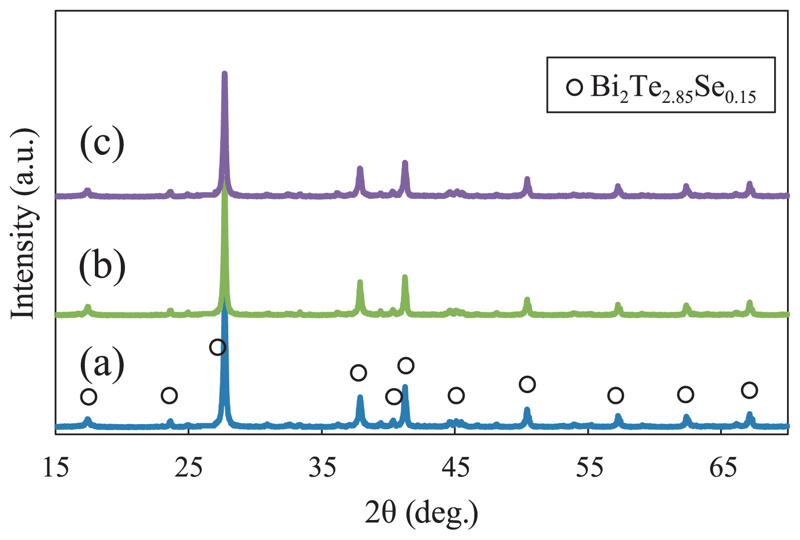
Fig. 3 shows the EPMA results of the samples SPSed at 300 °C. The different colors in the maps represent different composition (CP) levels. From the backscattered electron image (BEI) shown in Fig. 3 (a), where no Cu was doped, it can be found that there exist some dark regions in the matrix. In comparison with the distribution map of Te, these dark regions can be regarded as a Te-rich phase, which is considered to result from the vaporization or sublimation of Te from Bi2Te2.85Se0.15 matrix due to its high vapor pressure11). Bi and Se exhibited homogeneous distributions, as shown in Bi and Se maps. Fig. 3 (b) illustrates the maps of Cu-doped sample. Although Cu exhibited a low composition level, no severe segregation was observed and the Te-rich phase was still present in the matrix.

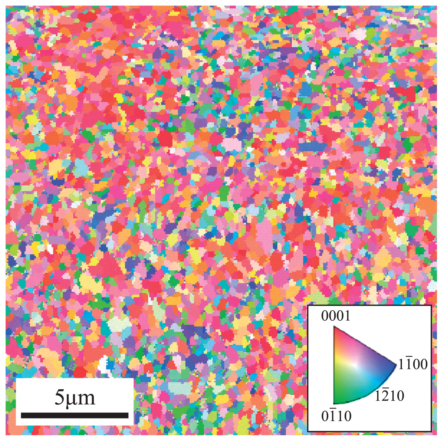
Fig. 4 shows the OIM map of the sample SPSed at 340 °C on its cross section perpendicular to the pressing direction. The sintered sample exhibited a fine microstructure with an average grain size of 0.4 μm. Fine-grained microstructures were also observed in the samples SPSed at other sintering temperatures. Furthermore, the SPSed sample still exhibited a preferred orientation of (0001) due to layered rhombohedral structure of Bi2Te3-based compound12), even though (0001) orientation in the SPSed sample is weaker than that in the hot-extruded sample6,13).
3.2 Thermoelectric properties
Fig. 5 shows the dependence of carrier concentration on Cu content. The carrier concentration exhibited a decreased tendency with increasing the Cu content in both sintering temperatures. This result contradicts the common opinion in which Cu acts as a donor of free electrons and should increase carrier concentration. The reason for the reduction of carrier concentration is likely related to the mechanical defects (Te vacancies [VTe] and anti-site defects [TeBi]) introduced by MA14,15). Oh et al. have proposed that the defects act as doping defects via the following equation16):
|
T
e
T
e
+
V
B
i
’’’
+
3
h
•
→
V
T
e
•
•
+
T
e
B
i
•
+
3
e
′ | (1) |
where h• is the produced hole; e′ is the produced electron, which can cause an increase in carrier concentration for n-type materials. Due to weak van der Waals bond between Te(1)–Te(1) layers12), the mechanical deformation during the MA and SPS processes promotes the formation of Te vacancies [VTe], anti-site defects [TeBi], and [e], as expressed in Eq. (1). It should be noted that the vaporization or sublimation of Te results in formation of many pores with sizes much larger than the vacancies and Te-rich phase with a micro scale in the matrix, as shown in Fig. 3. It is considered that there is no strong relationship between the vaporization of Te and Te vacancies, and the effect of these pores on the carrier concentration is not significant. Liu et al.10) have reported that the formation of [VTe] is limited due to the presence of Cu, which results in a reduction of [e], and thus causes decrease in carrier concentration in this work.
It has been confirmed that the donor-like defects ([VTe] and [TeBi]) can be reduced by annealing treatment15,17). Consequently, at a higher sintering temperature, fewer defects remain, which causes a shift of the reaction in Eq. (1) from the left to the right, resulting in an increase in [e]. Thus, when small amounts of Cu (x ≤ 0.015) were doped, the carrier concentration exhibited a higher level at 400 °C than that at 300 °C. As Cu content increases, it seems that the limitation of [VTe] by Cu becomes predominant, which results in significant decrease in carrier concentration at 400 °C. This may be possible because the diffusion of Cu occurs easily at a higher temperature.
Fig. 6 shows the dependences of the Seebeck coefficient and electrical resistivity on Cu content. The absolute values of the Seebeck coefficient increased with increasing Cu content, as shown in Fig. 6 (a). The change was larger at 400 °C than that at 300 °C. The Seebeck coefficient highly depends on carrier concentration, and it is determined by α ≈ γ − ln n18), where α, γ and n are the Seebeck coefficient, scattering factor, and carrier concentration, respectively. Thus, the variations of the Seebeck coefficient are in good agreement with the results of carrier concentration shown in Fig. 5.
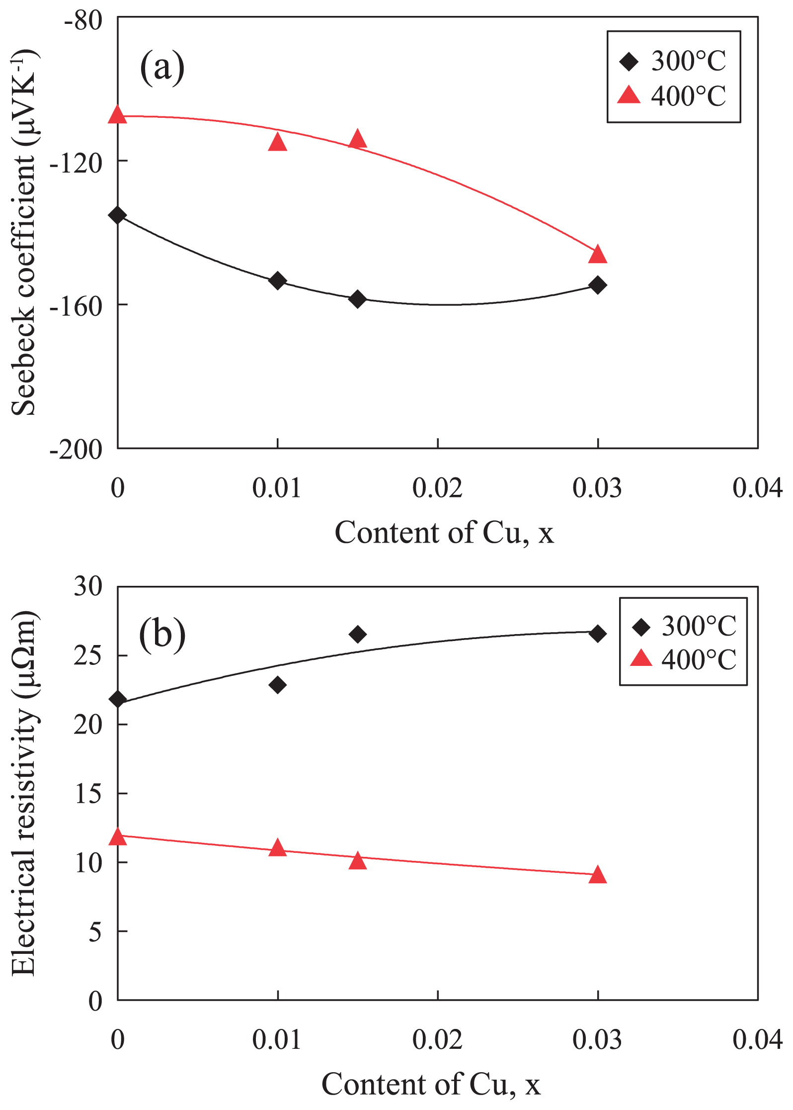
From Fig. 6 (b), it appears that the electrical resistivity does not change significantly with increasing Cu content. However, the electrical resistivity of the sample sintered at 300 °C was much higher than that sintered at 400 °C. This is mainly because that a lower sintering temperature leads to formation of a fine-grained microstructure, resulting in increase in scattering of carriers and thus electrical resistivity.
Fig. 7 shows the dependences of thermal conductivity and figure of merit ZT on Cu content. A slight change of thermal conductivity was found as the Cu content increased (Fig. 7 (a)), and the samples SPSed at 400 °C exhibited higher thermal conductivity than those SPSed at 300 °C. Thermal conductivity is related to electron-phonon interaction and it can be expressed according to the following equation19):
where κph and κel are lattice thermal conductivity and electron thermal conductivity, respectively. Higher thermal conductivity at 400 °C is due to larger grain sizes at higher sintering temperature, which causes the decrease in phonon scattering from grain boundaries and thus increase in thermal conductivity. As a result, a largest ZT value of 0.58 was obtained (Fig. 7 (b)) at room temperature for Cu0.03Bi2Te2.85Se0.15 sample SPSed at 400 °C.
Based on the above results, currently, we have tried to prepare CuxBi2Te2.85Se0.15 bulk materials by hot-extrusion method. The extruded samples exhibited high relative density of > 98 % and refined microstructure with a strong preferred orientation of (0001). Compared to the SPSed Cu0.01Bi2Te2.85Se0.15 sample, the extruded sample with the same composition exhibited a 2.5 times larger power factor (α2/ρ), which is determined by the Seebeck coefficient and electrical resistivity. Therefore, MA and hot-extrusion technique is a promising method to enhance the performance of n-type Bi2Te3-based thermoelectric materials.
4 Summary
Dense n-type CuxBi2Te2.85Se0.15 bulk thermoelectric materials were fabricated by MA and SPS technique. The SPSed samples exhibited fine-grained microstructure. At a lower sintering temperature of 300 °C, the effect of Cu doping on thermoelectric properties was not evident. At 400 °C, the carrier concentration was reduced significantly with increasing Cu content, and thus resulting in a significant increase in the absolute value of the Seebeck coefficient. However, the effect of Cu doping on electrical resistivity and thermal conductivity was not significant. An increase in dimensionless figure of merit ZT was found with increasing Cu content. A largest ZT value of 0.58 was achieved at room temperature for the Cu0.03 Bi2Te2.85Se0.15 sample sintered at 400°C.
Acknowledgements
The authors would like to thank Prof. Hiroyuki Kitagawa of Shimane University for his experimental supports and fruitful discussion. This work was supported in part by Japan Science and Technology Agency and the Amada Foundation.
References
- 1) J. T. Im, K. T. Hartwig, et al.: “Microstructural refinement of cast p-type Bi2Te3–Sb2Te3 by equal channel angular extrusion ”, Acta Mater., 52 (2004) 49–55.
- 2) P. J. Taylor, J. R. Maddux, et al.: “Room-temperature anisotropic, thermoelectric, and electrical properties…”, J. Appl. Phys., 85 (1999) 7807–7813.
- 3) W. M. Yim, F. D. Rosi: “Compound tellurides and their alloys for peltier cooling—A review”, Solid-State Electron., 15 (1972) 1121.
- 4) J. Y. Yang, T. Aizawa, et al.: “Thermoelectric properties of n-type (Bi2Se3)x(Bi2Te3)1−x prepared by bulk mechanical alloying and hot pressing”, J. Alloys Compd., 312 (2000) 326–330.
- 5) Y. Nagami, K. Matsuoka, et al.: “Preparation and Characterization of Bi0.4Sb1.6Te3 Bulk Thermoelectric Materials”, J. Electron. Mater., 43 (2014) 2262–2268.
- 6) Z. L. Wang, K. Matsuoka, et al.: “Extrusion behavior and thermoelectric properties of Bi2Te2.85Se0.15 thermoelectric materials”, Procedia Eng., (2014) 616–621.
- 7) T. E. Svechnikova, P. P. Konstantinov, et al.: “Physical Properties of Bi2Te2.85Se0.15 Single Crystals Doped with Cu, Cd, In, Ge, S, or Se”, Inorg. Mater., 36 (6) (2000) 556–560.
- 8) F. Wu, H. Song, et al.: “Effects of Ce, Y, and Sm doping on the thermoelectric properties of Bi2Te3 alloy”, Prog. in Nat. Sci.: Mater. Inter., 23 (4) (2013) 408–412.
- 9) J. L. Cui, L. D. Mao, et al.: “Thermoelectric properties of Cu-doped n-type (Bi2Te3)0.9(Bi2− xCuxSe3)0.1(x = 0–0.2) alloys”, J. Solid State Chem., 180 (12) (2007) 3583–3587.
- 10) W. S. Liu, Q. Zhang, et al.: “Thermoelectric Property Studies on Cu-Doped n-type CuxBi2Te2.7Se0.3 Nanocomposites”, Adv. Energy Mater., 1 (2011) 577.
- 11) Y. Suga, ed., Thermoelectric semiconductor, Tokyo: Makisyoten, (1966) 317.
- 12) J. R. Drabble, C. H. L. Goodman: “Chemical bonding in bismuth telluride”, J. Phys. Chem. Solids, 5 (1958) 142–145.
- 13) Z. C. Chen, K. Suzuki, et al.: “Microstructural features and deformation-induced lattice defects in hot-extruded Bi2Te3 thermoelectric compound”, Mater. Sci. Eng., A 500 (2009) 70–78.
- 14) J. Navrátil, Z. Starý, et al.: “Thermoelectric properties of p-type antimony bismuth telluride alloys prepared by cold pressing”, Mater. Res. Bull., 31 (1996) 1559–1566.
- 15) L. D. Zhao, B. P. Zhang, et al.: “Effects of annealing on electrical properties of n-type Bi2 Te3 fabricated by mechanical alloying and spark plasma sintering”, J. Alloys Compd., 467 (2009) 91–97.
- 16) M. W. Oh, J. H. Son, et al.: “Antisite defects in n-type Bi2(Te, Se)3: Experimental and theoretical studies”, J. Appl. Phys., 115 (13) (2014) 133706.
- 17) J. M. Schultz, J. P. Mchugh, et al.: “Effects of heavy deformation and annealing on the electrical properties of Bi2Te3”, J. Appl. Phys., 33 (1962) 2443.
- 18) X. D. Liu, Y. H. Park: “Structure and Transport Properties of (Bi1−xSbx)2Te3 Thermoelectric Materials Prepared by Mechanical Alloying and Pulse Discharge Sintering”, Mater. Trans., 43 (2003) 681.
- 19) T. S. Kim, I. S. Kim, et al.: “Thermoelectric properties of p-type 25 % Bi2Te3 + 75 % Sb2Te3 alloys manufactured by rapid solidification and hot pressing”, Mater. Sci. Eng., B 90 (2002) 42–46.