Abstract
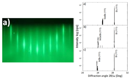
The single crystalline InSb and GaSb thin films on the same Si(111) substrate is an essence of CMOS device fabrication. In this study, the growth of InSb has been observed on InGaSb intermediate layer grown on High Quality (HQ) GaSb buffer layer of single crystalline nature. In this case, InxGa1–xSb was initially grown on HQ GaSb/Si(111)-√3 × √3-Ga surface following a two-step growth method. The controlled and precise flux ratio of Ga and Sb enabled HQ GaSb layer to grow without twins. For InxGa1–xSb intermediate layer, In ratio x ranged from 0.90 to 0.75 for samples S1–S4 with a step 0.05. To analyze the growth nature and surface morphology, Reflection High Energy Electron Diffraction (RHEED), Scanning Electron Microscopy (SEM), X-Ray Diffraction (XRD) have been performed and studied. It is concluded that InSb epitaxial surfaces have shown better smoothness and fewer defects towards Gallium increase. The growth nature in this case for both InSb epitaxial layer and InGaSb intermediate layer were coherent where HQ GaSb buffer layer was effective in decreasing twins. Some complementary samples were prepared to support the assumptions made before starting the experiments. Finally, the possibility of single crystalline InSb and GaSb thin films on the same Si(111) substrate has been demonstrated. [DOI: 10.1380/ejssnt.2018.20]