Abstract
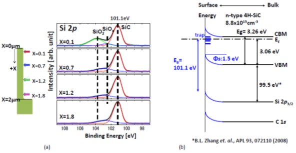
SiC trench structures having a width of 0.6 μm and a depth of 2.0 μm are fabricated by reactive ion etching (RIE) using a gas mixture of SF6, Ar, and O2. Further, SiC trench structures are cleaved to expose the sidewall for the channel region of a trench MOSFET. These structures were analyzed by pin-point photoelectron spectroscopy using a 100 nm soft-X-ray beam. It is observed that around 2 nm-thick homogeneous carbon-rich layer containing 1—2% F forms on the SiC sidewalls. This may be caused due to the re-deposition of RIE reaction products, CF4 and SiF4, under appropriate conditions to fabricate the trench walls that are approximately vertical using RIE. Further, a carbon-rich layer having a thickness of about 2.4 nm is also formed on the bottom of the SiC trench, suggesting the possibility of selective etching of Si from the SiC substrates. The position of the dominant peak that is associated with the SiC component remains constant regardless of the trench depth, suggesting homogeneous band bending due to the RIE defects, which may explain the reason for no variation being observed in the gate oxide/SiC interface trap density values. Further, the band bending of 1.50 eV that is observed on the sidewall can be attributed to a positively charged carbon vacancy (VC+). [DOI: 10.1380/ejssnt.2018.257]