Abstract
Microstructures were examined on the chip specimen of pure titanium with close-packed hexagonal (cph) structure (α-Ti, the shear strain, γ, is ~22), and those of pure iron (α-Fe, γ ≈ 7.5) and 0.83%C steel which had originally pearlite structure (γ ≈ 7.5) with body-centered cubic (bcc) structure by the FE-SEM/EBSP method and optical microscopy. The hardness of the chip specimens was also measured and compared to that of the original materials. UFGed materials could be produced at relatively small shear strain (~7.5) in pure iron and 0.83%C steel. The average grain diameter of the chip specimen was slightly larger in the 0.83%C, because lamellar cementite phase in original pearlite structure hindered the formation of submicron grains. The hardness of the chip specimens increased with increasing shear strain, and the hardness of the chip specimen with γ ≈ 7.5 (391 Hv) was ~4 times as much as that of the original material (93.9 Hv) in pure iron. However, it was impossible to produce the ultra-fine grained materials by machining of α-Ti even at γ ≈ 22. According to the experimental results obtained so far, the number of slip systems (crystal structure) as well as shear strain seems to be one of the important factors controlling the generation of equiaxed submicron grain structure. Higher stacking fault energy is favorable for cross-slip or climb of dislocations in dynamic recovery which probably governs the generation of submicron grains.
1. Introduction
For production of ultra-fine grained (UFGed) metals and alloys, machining is a unique severe plastic deformation (SPD) process which can impose a large shear strain up to ~20 on chips by a single cutting process, and is applicable to high-strength materials.1,2) Nano-structured materials often show very high strength without serious loss of ductility compared to the materials with deformed microstructure formed by usual processing.3,4) It is also known that UFGed materials have large internal friction.5,6) Therefore, strong particles which can be produced by milling of chips with UFGed structure are applicable as strengthening phase to the production of multi-functional metal matrix composites. Based on the microstructural observation using transmission electron microscopy (TEM) of thin foils, Ravi Shankar and his co-workers concluded that a large volume of equiaxed SMGs was obtained in the specimen with relatively small shear strain (γ), for example, ~5.2 for 6061-T6 alloy with face-centered cubic (fcc) structure7) and ~3.2 for α-Ti with close-packed hexagonal (cph) structure.8) Ni and his co-workers reported similar results on 1100 aluminum9) and pure Cu.10) According to the microstructural analysis by the FE-SEM/EBSP method,11,12) Tanaka et al.13,14) recently found that the chip specimen with γ ≈ 7.5 of the ferritic SUS430 (16Cr) steel with body-centered cubic (bcc) structure was principally composed of equiaxed submicron grains (SMGs). However, the chip specimens with shear strain (γ) up to ~10 of the 6061-T6 alloy as well as the chip specimen with γ ≈ 14 of the austenitic SUS304 (18Cr–8Ni) steel (fcc) had principally a deformed microstructure with elongated grains. Thus, there is controversy on the generation of UFGed materials by machining. Can machining really produce UFGed materials in any metals and alloys? It is necessary to examine the factors controlling the generation of UFGed materials in order to identify applicability of this technique. In this study, microstructures were examined on the chip specimens of pure titanium (α-Ti, the shear strain, γ, is ~22), pure iron (α-Fe, γ ≈ 7.5) and 0.83%C steel (γ ≈ 7.5) with pearlite structure by the FE-SEM/EBSP method and optical microscopy. The hardness of the chip specimens was also measured and compared to that of the original materials. Then, the factors controlling the generation of equiaxed SMG structure by machining were discussed on the basis of the experimental results obtained so far.
2. Experimental Procedure
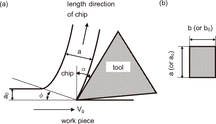
Pure titanium (α-Ti, 99.8 mass%Ti) with cph structure were supplied in the form of round bars with a diameter of 20 mm air-cooled after annealing at 963 K. Round bars with 20 mm diameter of pure iron pure iron (Fe - 0.03 mass%C) with bcc structure were air-cooled to 973 K after solution-heating for 7200 s at 1323 K and then furnace-cooled from 973 K to room temperature in order to produce ferrite single phase. Those of 0.83%C steel (Fe - 0.83 mass%C) were air-cooled to 973 K after solution-annealing for 3600 s at 1373 K and then furnace-cooled from 973 K to room temperature to generate pearlite structure. The microstructure of the heat-treated steel consisted of lamellar cementite (Fe3C) phase and ferrite matrix with bcc structure, accompanied by a small amount of pro-eutectoid cementite. The averaged grain size of the original material was 28 μm for α-Ti, 70 μm for pure iron and 80 μm for 0.83%C steel. The chip specimens were produced by dry cutting using a lathe and cutting tools of the same high-speed steel with a rake angle (α) of 4.8°. Table 1 reports the cutting conditions and geometry of resulting chip specimens in machining. The cutting depth (a0) and feed (b0) in machining, and the thickness (a) and width (b) of the chip specimens are also listed in the table. Figure 1 shows the schematic illustration of cutting process and the geometry of chip specimens. Relatively low cutting speed of Vg = 0.24 m/s was chosen to avoid excessive heating of chip specimens during machining. Two dimensional cutting was adopted for producing chip specimens in this study. The approximate shear strain (γ) in the central part of the chip specimens was calculated by the following equation.15)
|
γ = cotΦ + tan(
Φ–α
)
| (1) |
where Φ is the shear plane angle, and
|
tanΦ = (
a
0
/a
)
cosα/
[
1–(
a
0
/a
)
sinα
]
)
| (2) |
The thickness of chip specimens is in the range from 0.75 to 1.10 mm, and is much larger than the cutting depth (0.05 to 0.10 mm) (
Table 1). A small cutting depth may lead to a small value of shear angle (Φ) in the cutting process, which results in a large thickness of chip specimens.
Table 1. Cutting conditions and geometry of resulting chip specimens in machining.
| Material | Approximate shear strain (γ) | Cutting conditions | Geometry of chip specimens |
|---|
| Cutting depth (a0), mm | Feed (b0), mm | Thickness (a), mm | Width (b), mm |
|---|
| pure titanium | 22 | 0.05 | 0.55 | 1.10 | 0.20 |
| pure iron | 7.5 | 0.10 | 0.55 | 0.75 | 1.15 |
| 0.83%C steel | 7.5 | 0.10 | 0.55 | 0.75 | 0.55 |
In order to produce chip specimens with the same microstructure in the same material, the cutting conditions including the rake angle, the cutting depth, the feed and the cutting speed were kept constant during machining. The geometry of cross section in the chip was maintained during machining, because wear of cutting tools may affect the geometry of the chip specimen. Machining was repeated several times to produce continuous chips of at least 20 mm in length.
Misorientation (rotation angle, θ°) between neighboring grains in the chip specimens was examined by the FE-SEM/EBSP method, which is an orientation imaging microscopy (OIM).11,12) In SUS430 steel,14) ~90% in volume of the chip specimen with γ ≈ 7.5 had equiaxed SMG structure, while very small grains were observed near the surface contacting with cutting tool and a little larger grains were partly involved in the region near free surface. Similar result was obtained in the chip specimen with γ ≈ 22 in Inconel X-750 (NCF 750) alloy. In this study, microstructural analysis by the FE-SEM/EBSP method was at first made in a wide area of 200 μm × 200 μm in the middle part of chip specimens in the thickness direction, and the detailed analysis was carried out on the representative region with an area of 20 μm × 20 μm. According to the misorientation (θ), grain boundaries are conventionally classified into three categories, namely, small angle grain boundaries (2° ≤ θ < 5°), medium angle boundaries (5° ≤ θ < 15°) and large angle grain boundaries (θ ≥ 15°). Fractions of these grain boundaries were examined in chip specimens. The size range of grains or the averaged grain diameter was examined by the FE-SEM/EBSP method on 100 grains in each chip specimen. The hardness of original materials and chip specimens was also measured using a Micro Vickers Hardness Tester at the load of 0.98 N. The hardness was obtained as an averaged value over eight out of ten indentations by excluding the maximum and minimum values for each measurement.
3. Results and Discussion
3.1. Microstructures of Chip Specimens
Figure 2 shows the result of microstructural analysis in the chip specimen with γ ≈ 22 of pure titanium. The analyzed area is 20 μm × 20 μm. The length direction of the chip specimen (the direction of chip formation) is vertical. As shown in the image quality map (Fig. 2(a)), the chip specimen is principally composed of deformed microstructure with large elongated grains (~4 to ~40 μm in length and ~2 to ~15 μm in width) surrounded by large angle grain boundaries, which is similar to the one observed in the chip specimens of the SUS304 steel (γ ≈ 14) and 6061-T6 alloy (γ ≈ 10),14) although equiaxed SMGs of ~0.5 μm are partly observed between large grains in the inverse pole figure map (Fig. 2(b)). There are also many subgrains separated by small angle (2° ≤ θ <5°) or medium angle (5° ≤ θ < 15°) grain boundaries in large grains (Fig. 2(c)). The fractions of small angle, medium angle and large angle (θ ≥ 15°) grain boundaries are ~31%, ~32% and ~37%, respectively (Fig. 2(d)). The hardness of the chip specimens increased with increasing shear strain, and the hardness of the chip specimen with γ ≈ 22, 256 Hv, was considerably higher than that of the original pure titanium, 155 Hv.
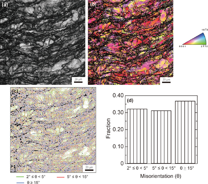
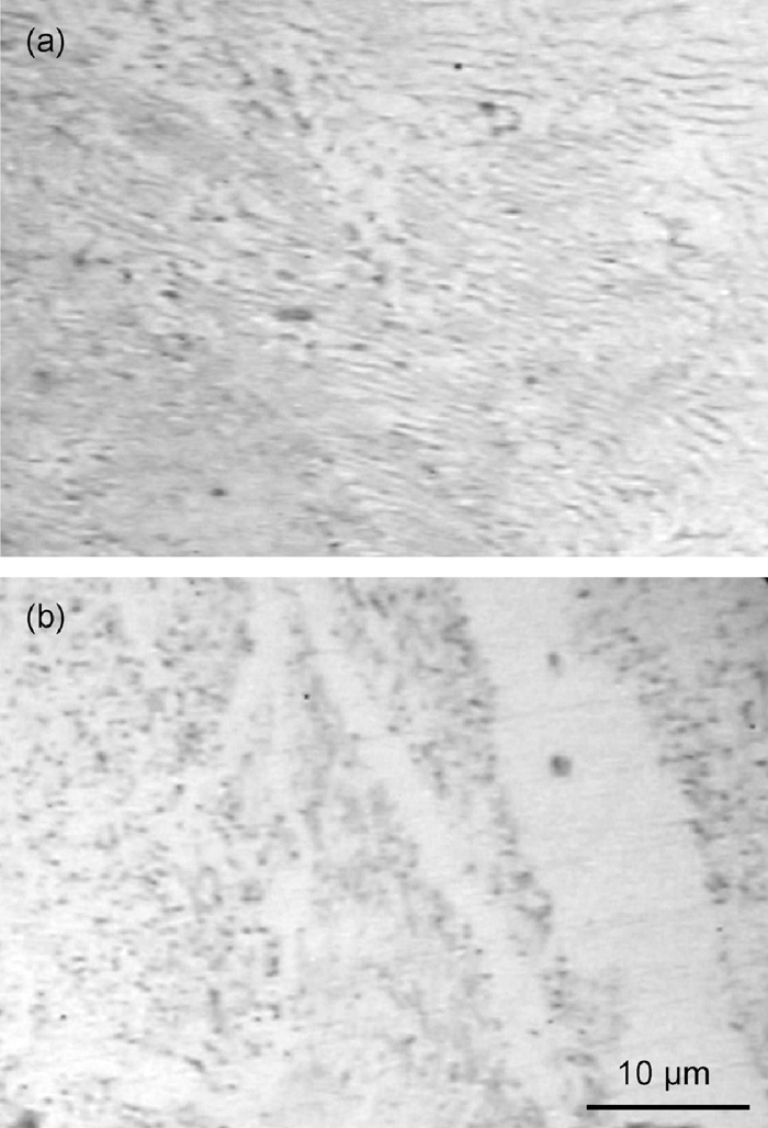
Figure 3 shows the result of microstructural analysis on the chip specimens with γ ≈ 7.5 of pure iron. At the lower magnification, very fine grains which are observed in the image quality map (Fig. 3(a)) have various orientations, as shown in the inverse pole figure map (Fig. 3(b)). This chip specimen is composed of equiaxed SMGs with the averaged grain diameter of ~0.5 μm (Figs. 3(c) and 3(d)), which are principally separated by large angle grain boundaries (Fig. 3(e)). The fraction of large angle grain boundaries is ~78% and that of medium angle grain boundaries is ~17%, while the fraction of small angle grain boundaries is only ~4.8% (Fig. 3(f)). The hardness of the chip specimens largely increased with increasing shear strain in pure iron. The hardness of the chip specimen with γ ≈ 7.5 was 391 Hv and ~4 times as much as that of the original pure iron, 93.9 Hv. In the chip specimen of 0.83%C steel with γ ≈ 7.5 (Fig. 4), there are dark regions and slightly bright regions in the image quality map (Fig. 4(a)) The dark regions seem to involve many areas in which crystallographic orientation is not known. The chip specimen is for the most part composed of equiaxed SMGs (Fig. 4(c)). The averaged grain diameter, ~0.7 μm, in the chip specimen of 0.83%C steel is slightly larger than that in the chip specimen of pure iron, because larger grains (a few micron meters in length) are partly observed in the former specimen (Fig. 4(d)). The fraction of large angle grain boundaries is ~60% (Fig. 4(f)) and this value is smaller than that of the chip specimen of pure iron (~78%). The hardness of the original 0.83%C steel was 283 Hv and was considerably higher than that of the original pure iron (93.9 Hv) because of existence of lamellar cementite phase. It is interesting to note that the hardness of the chip specimen with γ ≈ 7.5 of 0.83%C steel was 410 Hv and was only slightly higher than that of the chip specimen with γ ≈ 7.5 of pure iron (391 Hv).
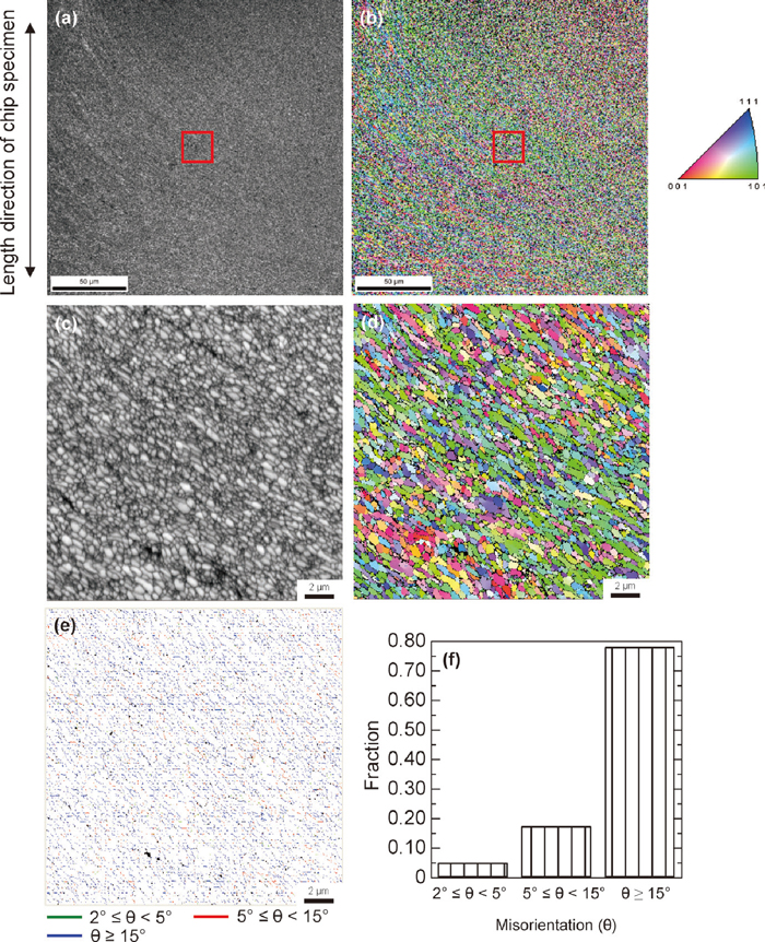
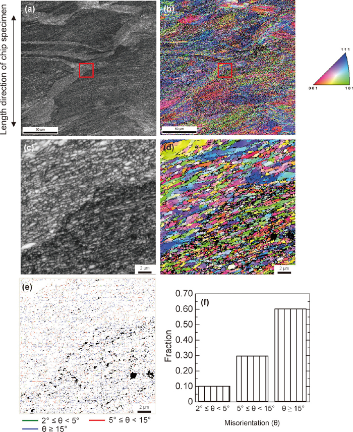
Figure 5 shows the microstructures of the original material and the chip specimen of 0.83%C steel. Pearlite structure with lamellar cementite phase is observed in the original material (Fig. 5(a)). However, pearlite structure is not clear in the chip specimen with γ ≈ 7.5 (Fig. 5(b)). The length direction of chip specimen is horizontal in this figure. Small granular precipitates together with precipitate-free zones running in the vertical direction are visible in the chip specimen. Lamellar cementite phase becomes an obstacle to impede the movement and rearrangement of dislocations which are introduced by machining. At the same time, a part of cementite lamellar phase may be cut by dislocations to form segments or granular particles, or may dissolve into ferrite matrix during heating in the cutting process. These processes may lead to slightly larger grain size (~0.7 μm) in the chip specimen of 0.83%C steel compared to that (~0.5 μm) in the chip specimen of pure iron (Fig. 2) at the same shear strain of ~7.5.
The chip specimens with shear strain (γ) of ~7.5 of the materials with bcc structure such as pure iron (Fig. 3), 0.83%C steel (Fig. 4) and SUS430 steel14) were principally composed of equiaxed SMGs mostly separated by large angle grain boundaries (θ ≥ 15°). Similar microstructure was observed in the chip specimen of Inconel X-750 (NCF 750) alloy at much larger strain of ~22. However, the chip specimen of pure titanium exhibited deformed microstructure with elongated grains and sub grains even at the shear strain of ~22 (Fig. 2). The stacking fault energy (SFE) for pure titanium (α-Ti) is 0.31 J/m2 16) and is higher than the SFE of pure iron (0.20 J/m2).17) The SFE of 0.83%C steel and SUS430 steel is considered to be as high as that of pure iron, and the SFE of 6061-T6 alloy is probably almost the same as that of pure Al (0.20 J/m2).17) Much lower SFE was reported in the solution-treated specimen of Inconel X-750 alloy (0.09 J/m2),18) while the SFE of the SUS304 steel was estimated to be 0.011 J/m2 according to Breedis.19)
Temperature measurements of chips were not made in this study. However, the maximum temperature of chips during machining can be deduced to some extent from the maximum tool temperature in the published data.20) The maximum chip temperature seems to be in the range from ~0.4Tm to ~0.5Tm in the cutting process of these alloys.14) Thus, machining process essentially belongs to hot deformation, although the heating time of chips may be very short (shorter than ~0.2 s).14) McQueen21) reported that the degree of dynamic recovery observed in metals at a certain value of strain rate and homologous temperature depends on the relative abilities of dislocations to leave the slip planes. This has been found to be limited in metals of low SFE because the dislocations are extended on the slip plane and require thermal activation to constrict in order to cross-slip or climb. This suggests that SMGs are formed by dynamic recovery in the materials with bcc structure, 6061-T6 alloy and pure titanium with high SFE, because high SFE is favorable for cross-slip or climb of dislocations in dynamic recovery process. However, nano-structured materials were produced only in the materials with bcc structure and in NCF 750 alloy with the lower SFE and fcc structure.
The number of slip systems in metals and alloys with bcc structure is 48, and is larger than that in the materials with fcc structure (12). Frequent cross-slip or climb of dislocations in more slip systems may increase the opportunity of interactions between dislocations in the materials with bcc structure, which may lead to the enhanced tangles of many dislocations in different slip systems introduced by machining. About ECAP for production of UFGed microstructure in high-purity aluminum,22) the route BC seems to be favorable for operating many slip systems to produce high misorientation boundaries as a result of accumulation and dynamic recovery of dislocations during ECAP. The number of slip systems may be restricted in comparison with ECAP with route BC, when materials are subjected to a simple shear deformation process in the chip formation during machining. Accumulation of slip dislocations may occur more easily in metals and alloys with bcc structure, which have more slip systems than those with fcc or cph structure. This is why the chip specimen principally composed of equiaxed SMGs was produced at relatively small shear strain (~7.5) by dry cutting of the materials with bcc structure. Thus, the number of slip systems (crystal structure) as well as the shear strain seems to be one of the important factors controlling the generation of equiaxed SMG structure. Swaminathan et al.23) reported that equiaxed SMG structure in an OFHC Cu (SFE is 0.050 J/m2) was caused by dynamic recrystallization. However, dynamic recovery may also lead to the formation of SMGs even in NCF 750 alloy and SUS304 steel with low SFE and fcc structure, because migration of atoms in a large scale by grain-boundary diffusion or short-circuit diffusion through dislocation cores may be unrealistic for nucleation of equiaxed SMGs in a very short period of cutting.
Ravi Shankar and his co-workers7,8) claimed that a large volume of equiaxed SMGs was obtained in the specimens with relatively small strains (γ ≈ 5.2 for 6061-T6 alloy and γ ≈ 3.2 for α-Ti). Similar results were reported by Ni and his co-workers.9,10) These are probably because they examined the microstructures in a relatively small area of each chip specimen.1,2,7,8,9,10) In the preparation of thin foils for TEM, the region that involves a lot of lattice defects such as grain boundaries and dislocations is in energetically high state and may be selectively polished electrolytically to the thickness that is transparent by electron beam. However, such an area does not represent the microstructure of the chip specimen. For the microstructural analysis of chip specimens by the FE-SEM/EBSP method or by TEM, it is necessary to confirm how large area one observes in the analysis.
4. Conclusions
UFGed materials could be produced at relatively small shear strain (~7.5) in the materials with bcc structure such as pure iron and 0.83%C steel compared to NCF 750 alloy (~22) in the previous study. Further, the average grain diameter of the chip specimen was slightly larger in the 0.83%C, because lamellar cementite phase in original pearlite structure became an obstacle in the formation of submicron grains (SMGs). The hardness of the chip specimens increased with increasing shear strain, and the hardness of the chip specimen with γ ≈ 7.5, 391 Hv, was ~4 times as much as that of the original material, 93.9 Hv, in pure iron. However, it was impossible to produce the UFGed materials by machining of α-Ti with cph structure even at a large shear strain (γ) of ~22. According to the experimental results obtained so far, the number of slip systems (crystal structure) as well as shear strain seems to be one of the important factors controlling the generation of equiaxed SMG structure. Higher stacking fault energy (SFE) is favorable for cross-slip or climb of dislocations in dynamic recovery which probably governs the generation of SMGs.
Acknowledgements
The authors thank Ms R. Yoda, Kobelco Research Institute Inc., for microstructural analysis of chip specimens by the FE-SEM/EBSP method, and Mr. R. Kato, Research Assistant, and Mr. T. Hino, Student of Graduate School, of Akita University for their assistance in machining experiments.
References
- 1) T. L. Brown, S. Swaminathan, S. Chandrasekar, W. D. Compton, A. H. King and K. P. Trumble: J. Mater. Res., 17 (2002), 2484.
- 2) S. Swaminathan, M. Ravi Shankar, S. Lee, J. Hwang, A. H. King, R. F. Kezar, B. C. Rao, T. L. Brown, S. Chandrasekar, W. D. Compton and K. P. Trumble: Mater. Sci. Eng. A, 410 (2005), 358.
- 3) B. Q. Han, E. J. Lavernia and F. A. Mohamed: Metall. Mater. Trans., 35A (2004), 1343.
- 4) H. W. Höppel and R. Z. Valiev: Z. Metallkd., 93 (2002), 641.
- 5) R. R. Mulyukov, N. A. Akhmadeev, R. Z. Valiev and S. B. Mikhailov: Mater. Sci. Eng. A, 171 (1993), 143.
- 6) Y. Koizumi, M. Ueyama, N. Tsuji, Y. Minamino and K. Ota: J. Alloy Comp., 355 (2003), 47.
- 7) M. Ravi Shankar, S. Chandrasekar, W. D. Compton and A. H. King: Mater. Sci. Eng. A, 410 (2005), 364.
- 8) M. Ravi Shankar, R. Verma, B. C. Rao, S. Chandrasekar, W. D. Compton, A. H. King and K. P. Trumble: Metall. Trans., 38A (2007), 1899.
- 9) H. Ni and A. T. Alpas: Mater. Sci. Eng. A, 361 (2003), 338.
- 10) H. Ni, M. Elmadagli and A. T. Alpas: Mater. Sci. Eng. A, 385 (2004), 267.
- 11) B. L. Adams, S. I. Wright and K. Kunze: Metall. Trans., 24A (1993), 819.
- 12) D. J. Prior, A. P. Boyle, F. Brenker, M. C. Cheadle, A. Day, G. Lopez, L. Peruzzo, G. J. Potts, S. Reddy, R. Spiess, N. E. Timms, P. Trimby, J. Wheeler and L. Zetterström: Am. Mineralogist, 84 (1999), 1741.
- 13) M. Tanaka, R. Kato, J. Kobayashi and R. Yoda: ISIJ Int., 48 (2008), 815.
- 14) M. Tanaka, R. Kato, T. Fujita and R. Yoda: ISIJ Int., 51 (2011), 1142.
- 15) T. Baumeister: Marks’ Standard Handbook for Mechanical Engineers, Section 13, 7th ed., McGraw-Hill, Kogakusha, Tokyo, (1967), 69.
- 16) Z. Guo, A. P. Miodownik, N. Saunders and J-Ph. Schille: Scr. Mater., 54 (2006), 2175.
- 17) R. J. McElroy and Z. C. Szkopiak: Int. Metall. Rev., 17, (1972), 175.
- 18) R. A. Mulford: Acta Metall., 27 (1979), 1115.
- 19) J. F. Breedis: Trans. Metall. Soc. AIME, 230 (1964), 1583.
- 20) T. H. C. Childs, K. Maekawa, T. Obikawa and Y. Yamane: Metal Machining – Theory and Applications, Arnold, London, (2000).
- 21) H. J. McQueen: Metall. Trans. A, 8A (1977), 807.
- 22) M. Furukawa, Y. Iwahashi, Z. Horita, M. Nemoto and T. G. Langdon: Mater. Sci. Eng. A, 257 (1998), 328.
- 23) S. Swaminathan, M. Ravi Shankar, S. Lee, J. Hwang, A. H. King, R. F. Kezar, B. C. Rao, T. L. Brown, S. Chandrasekar, W. D. Compton and K. P. Trumble: Mater. Sci. Eng., A410–411 (2005), 358.