Ex Situ Electron Microscopy Study of the Lithiation of Single-Crystal Si Negative Electrodes during Charge Reaction in a Lithium–Ion Battery
2019 年 60 巻 11 号 p. 2328-2335
詳細
2019 年 60 巻 11 号 p. 2328-2335
Silicon (Si) has attracted considerable interest as a negative electrode material for next-generation lithium (Li)–ion batteries because of its high capacity density. In this study, ex situ electron microscopy was applied to observe Si negative electrodes under different charge states within an actual battery structure to reveal the Li intrusion direction and the effects of Li concentration on the electrode structure. All of the processes from disassembly of the charged battery and preparation of specimens for use in electron microscopy observation to specimen transport to the electron microscopes were performed under non-atmospheric exposure conditions. The orientation of the single-crystal Si powder in the charged state was observed by electron backscatter diffraction, indicating that lithiation occurred preferentially along the (110) plane of Si. The initial stage of amorphization was observed by high-angle annular dark field-scanning transmission electron microscopy, demonstrating that the Li atoms occupied the tetrahedral sites of Si crystals, and that the crystal structure was destroyed via the severing of Si–Si bonds between the {111} planes. During the charge reaction, Li occupied the tetrahedral sites via intrusion along the ⟨110⟩ direction of Si, and amorphization proceeded as the Li concentration increased. Thus, the amorphous region grew preferentially in the ⟨110⟩ direction of Si.

Lithium (Li)–ion secondary batteries are used in many applications, including electric vehicles (EVs) and various types of mobile electronic devices. For EV batteries, the development of materials with high capacities is essential because battery discharge capacity directly affects the driving range of the vehicle.1) Compared to conventional carbon materials, which store a large amount of Li when charged, silicon (Si) has attracted considerable attention as a negative electrode material because it is expected to increase the capacity-to-weight ratio by approximately 10 times compared to carbon.2) Although studies on the practical applications of batteries with Si negative electrodes are underway, basic microstructural analyses of Si and Li during electrochemical reactions remain insufficient. Compared to solid-state reactions at high temperature, anisotropy of the reaction with respect to crystallographic orientation has frequently been reported. In this case of electrochemical lithiation, atomic-level studies based on first-principles calculations and other approaches have suggested that the lithiation of Si crystals occurs preferentially in the {110} plane of Si, ultimately leading to amorphization.3–6) As the Li concentration increases, Li diffuses along the ⟨110⟩ direction of Si to occupy the tetrahedral sites of the {110} plane of Si, and amorphization occurs as zigzag chains are cut through the crystal structure via the destruction of Si–Si bonds between the {111} planes. In another study, single-crystal Si nanopillars with different crystal orientations were prepared, and their lithiation process was investigated with in situ scanning electron microscopy (SEM).7) The authors found that the swelling rate of the amorphous Li–Si phase (a-Li–Si) differed based on the crystallographic orientation, with the ⟨110⟩ direction exhibiting the fastest swelling rate. This orientation-dependent anisotropy of the amorphous phase formed during the lithiation of Si crystals and its swelling rate were also clarified in an investigation of the charge reaction of single-crystal Si nanowires with ⟨100⟩, ⟨110⟩, ⟨111⟩, and ⟨112⟩ orientations with respect to the axial direction.8) Although studies based on nuclear magnetic resonance9,10) and experiments on special Si structures11–13) have also been reported, no atomic-level observations of Li intrusion and the resulting structural changes in Si negative electrodes within actual battery structures have been reported.
In recent years, microscopic analyses using SEM, scanning transmission electron microscopy (STEM), and focused ion beam (FIB) have matured, and it has become possible to visualize and analyze the microstructures of composite materials from the micron level to the atomic level. The detection of light elements including Li has also become relatively easy because of improvements in the sensitivity of electron energy loss spectrometry (EELS) at the atomic level, and limited examples of in situ TEM observation have even been reported.14,15) It is important to clarify the causal relationship between the performance of functional materials and their microstructures using electron microscopy. Furthermore, it is necessary to enhance the use of electron microscopy in the analysis of the reactions that occur in Li–ion batteries using actual battery structures.
Since the materials used in Li–ion batteries are generally extremely active when exposed to moisture and air, it is difficult to know how long the microstructure remains stable when a battery in a charged state is exposed to the atmosphere. Thus, when observing and analyzing actual batteries, it is necessary to conduct ex situ experiments under strictly controlled environments that prevent the battery components from contacting the atmosphere during all processes, including battery disassembly, the preparation of specimens for electron microscopy, and specimen transport. For this reason, in this study, all processes from the preparation of charged Si powder specimens for electron microscopy to specimen transport were performed under non-atmospheric exposure conditions. After preparing negative electrodes using Si powder, the electrodes were charged through assembly in an Li–ion battery. After battery disassembly, the microstructural changes from the micron level to the atomic level were investigated by ex situ SEM and ex situ STEM observation.
The materials used to create the Li–ion secondary battery and the mixing ratios used when preparing the electrodes are described in this section. To produce the negative electrode, a copper (Cu) foil with a thickness of 20 µm was coated by Si powder: acetylene black: polyvinylidene fluoride (80:10:10 mass%), dried, and then pressed to form the electrode. The Si powder, which served as the active material of the negative electrode, was comprised of single crystals with an average particle size of 10 µm. The coating density was 2.1 mg/cm2 per unit area. An Li counter electrode half-cell formed from Li metal foil served as the positive electrode. The cell structure was created using a polyethylene separator with a thickness of 20 µm. Coin-type batteries were prepared by punching the electrodes to φ16 mm. Figure 1 shows a coin battery fabricated in this manner. The electrolytic solution was prepared by mixing 1 mol/L LiPF6 electrolyte in a solvent consisting of ethylene carbonate and diethylene carbonate (1:1 by volume).
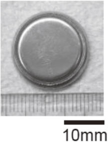
Image of the coin-type battery.
An electrochemical interface (CompactStat, Ivium Technologies) was used to charge the battery. In this study, to evaluate the theoretical capacity of the Li–ion secondary battery with a Si negative electrode, the state of charge (SOC) was determined from the mixing amount assuming 4.2 Ah/g as the upper limit in the fully charged state. Multiple sample batteries were prepared and charged once to SOC = 0% (before charging), 20%, 40%, 60%, 80%, or 100% (fully charged) and used in subsequent observations.
Figure 2 shows the charging curve of the battery charged to SOC = 100%. The voltage decreased sharply at the onset of charging, and the battery was charged to 4.2 Ah/g by capacity, which was defined as SOC = 100%. The potential at SOC = 100% was essentially 0 V. Immediately after charging, the coin batteries were disassembled in a glovebox in which the atmosphere had been replaced with highly pure Ar gas. The atmosphere in the glovebox was kept at a dewpoint of −80°C or less and an oxygen concentration of 1 ppm or less. Only the separated negative electrode was sampled from each disassembled battery. After disassembly, the negative electrode was cleaned three times with dimethyl carbonate and used in the analysis.

Charging curve of an Si negative electrode.
Cross sections of the negative electrodes were prepared using an ion milling system (Hitachi, IM4000) and observed by SEM (Hitachi, S-4800). A dedicated jig referred to as a transfer vessel was used to transfer the negative electrode in the charged state to the ion milling system. The closed structure of this transfer vessel maintained an inert atmosphere or vacuum around the specimen, making it possible to perform all processes from the transfer of the electrode to the ion milling system to the completion of processing without exposing the electrode to the atmosphere. After the coin battery was disassembled in the glovebox, it was placed in the transfer vessel of the ion milling system, and cross-sectional milling was carried out at a voltage of 4.0 kV and a current of 0.2 mA. Immediately after cross-sectional milling, the specimen was transferred to the microscope for SEM observation. It should be noted that the effect of the atmosphere on the charged negative electrodes was investigated to understand the effectiveness of the transfer vessel. A carbon negative electrode was fully charged to SOC = 100% and observed by SEM using the transfer vessel. After removing the specimen from the SEM chamber, it was exposed to the atmosphere for 1 min and then observed again by SEM for comparison. All SEM observations were performed at an accelerating voltage of 1.2 kV.
To investigate the effects of charging on the microstructure of the Si powder in the negative electrodes, specimens with different SOCs (0%, 20%, 40%, 60%, 80%, and 100%) were observed by SEM using the same procedure described above. To determine the relationship between lithiation and the crystallographic orientation of the Si powder, the crystallographic orientation of a Si negative electrode charged to SOC = 40% was analyzed by EBSD with OIM Analysis software (TSL).
2.4 TEM and STEM observationThe sample with SOC = 40% was analyzed by TEM and spherical aberration-corrected STEM at an accelerating voltage of 200 kV using a transmission electron microscope (JEOL, ARM200F). Composition analysis was carried out using EELS. Thin-film specimens were prepared with a FIB device (FEI, VERSA 3D) and transported to the microscope using a transfer vessel, as for the SEM analyses. Since the sample holder structures of the transfer vessels differed between SEM and TEM; thus, to prevent exposure to the atmosphere when transferring specimens between devices, the transfer vessel was returned to the glovebox, and the sample was placed in a different transfer vessel while still in the glovebox. The transfer vessel was not a commercial product, but it developed by JFE Techno Research was used.
Figure 3 shows SEM images of carbon negative electrodes with SOC = 100% for specimens before and after exposure to atmosphere for 1 min. By observing the same field of view on the sample before and after exposure to atmosphere, the Li that had lithiated in the carbon was shown to precipitate as a hydroxide via reaction with the atmosphere (Temperature: 298 K, Humidity: 45%). Thus, the charged negative electrodes were clearly degraded by atmospheric exposure for even a short period of time. This demonstrates that conducting battery disassembly and sample transfer for microscopy in an inert glovebox is an effective strategy for observing the microstructures of negative electrodes containing active Li.

Cross-sectional SEM images of a carbon electrode in the fully charged condition (a) before and (b) after exposure to the atmosphere for 1 min. For the image in (a), the sample was disassembled, cleaned, and dried in a glovebox; transferred to the ion milling system in a transfer vessel; and then transferred again to the SEM instrument in a transfer vessel after cross-sectional milling. For the image in (b), the sample in (a) was removed from the microscope and allowed to stand in the open atmosphere for 1 min.
Figure 4 shows the SEM mages of Si negative electrodes charged to various SOCs between 0% (before charging) and 100% (fully charged). The images, which show the entire electrode thin film, indicate increasing swelling of the Si powder with increasing SOC due to lithiation during charging. The swelling of the Si powder began at SOC = 40%, and the thin-film thickness at SOC = 100% [Fig. 4(f)] was approximately 5 to 6 greater than that at SOC = 0% [Fig. 4(a)]. The delamination of the Si powder from the Cu foil collector resulting from swelling was also observed in the regions indicated by white circles in the images of electrodes with SOC = 60% [Fig. 4(d)] and SOC = 80% [Fig. 4(e)]. Figures 4(g)–(l) show enlarged SEM images of the interior of the Si powder in Figs. 4(a)–(f), respectively. No major differences in Si grains were observed between the electrodes with SOC = 20% [Fig. 4(h)] and SOC = 0% [Fig. 4(g)]. However, linear parts with bright contrast are observed in the Si grains in the image of the specimen with in SOC = 40% [Fig. 4(i)], indicating that the structure of Si was changed during charging as a result of lithiation. As shown in Figs. 4(j)–(l), Si grain refinement resulting from lithiation was observed in specimens with SOC ≥ 60%, and the Si grains could no longer maintain their shape. At SOC = 100%, almost all Si grains were refined. As the SOC increased, the increasing refinement of Si grains was accompanied by the appearance of regions of decreased adhesion between Si grains. Thus, volumetric swelling resulting from lithiation caused grain refinement by destroying the Si grains, resulting in a rapid decrease in capacity.

Cross-sectional SEM images of Si negative electrodes with different SOCs: (a) and (g) 0% (before charging); (b) and (h) 20%; (c) and (i) 40%; (d) and (j) 60%; (e) and (k) 80%; and (f) and (l) 100% (fully charged). (g) to (l) show enlarged SEM images of the interior of the Si powder depicted in (a) to (f).
Figure 5 shows an enlarged view of an Si grain in an electrode with SOC = 40% [as observed in Fig. 4(i)]. As shown by the arrows, the linear parts caused by lithiation appear to have either a mutually parallel or an approximately 90° orientational relationship. Lithiation appears to progress in an anisotropic manner with respect to the crystallographic orientation of Si, suggesting the existence of a correlation between the intrusion path of Li and the crystallographic orientation. To confirm this, crystallographic orientation was analyzed by EBSD.

Enlarged SEM image of the interior of the Si powder (SOC = 40%) depicted in Fig. 4(i).
Figure 6 shows an SEM image, inverse pole figure (IPF) map, and schematic diagram of Li intrusion in a Si grain based on the Si crystal lattice. As shown by the arrows in Fig. 6(a), many linear parts propagated in a mutually parallel manner inside the Si grain, and the lithiation displayed anisotropy, as in Fig. 5. The (001) plane of Si was observed in the IPF map [Fig. 6(b)], indicating that the Si grain was a single crystal. Furthermore, the linear parts had low image quality (IQ) values and appeared black. These results indicate that the linear parts caused by lithiation propagated along the (110) plane of Si, and it is thought that Li intrusion occurred in the ⟨110⟩ direction, as shown schematically in the Si crystal lattice in Fig. 6(c). It should be noted that the grain shown in Fig. 6 was selected because its measurement surface was easy to examine based on the EBSD results and the analyses of multiple Si grains. Yang et al. prepared single-crystal Si nanowires with orientations of ⟨100⟩, ⟨110⟩, ⟨111⟩, and ⟨112⟩ with respect to the axial direction and investigated the orientation dependency of volumetric swelling accompanying lithiation during charging.8) The cross-sectional observation of the Si single-crystal nanowires in which lithiation had occurred during charging indicated that volumetric swelling caused by lithiation displayed anisotropy, and swelling occurred preferentially in the ⟨110⟩ direction (⟨111⟩ up to 20%, ⟨110⟩ up to 170%). This suggests that the diffusion of Li in the ⟨110⟩ direction occurs rapidly, which is consistent with the abovementioned analysis of crystallographic orientation. Therefore, the diffusion path of Li was evaluated in greater detail using TEM and STEM observation.

(a) Cross-sectional SEM image, (b) Inverse pole figure (IPF) map, and (c) Schematic diagram of Li intrusion into the Si crystal lattice. When the observed plane of Si is (001), Li intrusion into Si occurs along the (110) plane.
Figure 7 shows a TEM image of an Si grain in an electrode with SOC = 40% observed in the [110] direction along with electron diffraction (ED) patterns of regions (i) and (ii) in the TEM image. Elongated plate-like structures with widths of 100 to 200 nm can be observed in the TEM image. This width is almost identical to the widths of the lithiated linear parts observed by SEM, indicating that these plate-like structures were lithiated regions. The lattice reflection of Si can be observed in the ED pattern of region (i); however, a halo pattern indicative of an amorphous phase is observed in the pattern of the plate-like structure in region (ii). The ED pattern of region (i) suggests that the plate-like structure indicated by the arrows in the figure formed parallel to the $[\bar{1}10]$ direction. As mentioned earlier, in the IPF map [Fig. 6(b)], the linear parts had low IQ values and appeared black. The TEM results suggest that these features were caused by low crystallinity resulting from the amorphization of the linear parts via lithiation.

Cross-sectional TEM image showing the linear parts of Si in the sample with SOC = 40% along with the ED patterns obtained in regions (i) and (ii).
Figure 8(a) shows a high-angle annular dark-field (HAADF) STEM image of an Si grain in an electrode with SOC = 40%, while Fig. 8(b) shows the STEM-EELS analysis results obtained in the same field of view. The contrast of a HAADF-STEM image is proportional to the second power of the atomic number z; thus, the white areas of the HAADF-STEM image in Fig. 8(a) are Si (z = 14). The Li map in Fig. 8(b) indicates the presence of Li in the plate-like structure, as highlighted in red. From the EELS spectra measured in regions (i) and (ii) in Fig. 8(b), spectra in the Li energy range can be observed in both, but in comparison with region (i), a high spectrum is also observed in the Li–K energy range in region (ii). These results suggest that the plate-like structures contain a high content of Li compared to Si. Combined with the ED pattern of region (ii) in Fig. 7, the EELS results indicate that the plate-like structures underwent amorphization as a result of the high Li concentration. Figure 8(b) also showed differences in Li concentration within the red regions, particularly at the intersections between the plate-like structures. The amorphization of Si crystals via lithiation is a well-known phenomenon, and if the Li concentration increases after amorphization, a Li15Si4 phase (Cu15Si4 prototype, space group I43d) is formed.5) Based on the in situ TEM observation of lithiation during the charging reaction of Si, Wang et al. proposed a two-phase formation process of the a-Li–Si phase accompanying increasing Li concentration (lithiation).16) These structural changes during the electrochemical reaction caused by increasing Li concentration occur in a non-equilibrium state; thus, a condition in which the composition contains different Li concentrations might also exist in the non-equilibrium state accompanying concentration until crystallization is achieved.

(a) Cross-sectional HAADF-STEM image and (b) STEM-EELS map analysis result (red: Li, blue: Si) of Si in the sample with SOC = 40%. The EELS spectra obtained in regions (i) and (ii) are also shown on the right side (b).
Figure 9(a) shows a high-resolution TEM image of the linear structure surrounded by the white square in Fig. 7. This linear structure is in contact with the plate-like structure and has a small width, as shown in Fig. 7. Thus, this structure is considered to show the initial stage of Li intrusion into the Si crystal lattice. The image in Fig. 9(a) also shows the disordering of the Si crystal lattice with a width of approximately 2 nm. Figure 9(b) shows an enlarged HAADF-STEM image of the region enclosed in the white square in Fig. 9(a). The dark contrast observed along the {111} plane in Fig. 9(b) corresponds to the disordered region of the Si crystal lattice. This indicates that the Li concentration in this region was high in comparison to the surrounding area, and that Li intrusion was accompanied by the destruction of the Si crystal lattice.

Figure 10(a) shows low-pass filtered HAADF-STEM image of Fig. 9(b), while Fig. 10(b) shows a schematic diagram of the Si crystal lattice observed from the [110] direction. Fourier power spectrum image of Fig. 9(b) is inserted in Fig. 10(a). White circle denotes the information limit. Si–Si dumbbells with sizes of 0.136 nm were clearly observed in the Si crystal lattice. Some of the Si–Si dumbbells remained in the region where the Si lattice was disordered by Li intrusion. Thus, this disordering of the Si crystal lattice was considered to be the initial stage of amorphization driven by the increase in Li concentration. Despite the fact that the Si crystal lattice was not disordered in the region marked by the white square in Fig. 10(a), particulate contrast was observed at the tetrahedral sites, suggesting the possibility of Li atoms. As indicated by the yellow lines in Fig. 10(b), the Li atoms intruded between the {111} planes of Si.

(a) Low-pass filtered HAADF-STEM image of Fig. 9(b). Particulate contrast indicative of Li atoms is observed at tetrahedral sites (indicated by the white square). (b) Schematic diagram of the Si crystal lattice observed from the [110] direction. The yellow lines indicate the {111} planes between which the Li atoms intrude.
Figure 11(a) shows a schematic diagram of the amorphization process of the Si crystal lattice by the intrusion of Li based on the results of this study. As indicated in the schematic, Li intrudes along the ⟨110⟩ direction and occupies the tetrahedral sites of the {110} plane of Si. As the concentration of Li increases, amorphization proceeds via the destruction of the Si crystal structure as the Si bonds between the {111} planes are severed. This process can be visualized as cutting along a zigzag pattern, as indicated by the arrows in Fig. 11(a). Si–Si dumbbells were reported to remain when the crystal structure was decomposed into zigzag chains in the initial stage of lithiation because the {111} planes of Si have low surface energy compared to other crystal planes and thus cleave more easily.9) Ab initio calculations of hydrogen injection into Si indicated that the Si bonds between the {111} planes were destroyed by hydrogen atoms after hydrogen injection, resulting in the propagation of fine cracks in the {111} plane.17) The interstitial spacing along the ⟨110⟩ direction is large in Si and other substances with diamond structures, providing ion channels during ion injection processes.18) If the Li concentration in Si increases because of an increase in charging depth, an amorphous phase is thought to be formed by the destruction of the Si crystal lattice resulting from increased Li intrusion into tetrahedral sites. This region of this amorphous phase will expanded via preferential growth in the ⟨110⟩ direction, as shown in the schematic diagram presented in Fig. 11(b). The anisotropy of the linear parts with sizes of several microns (see Figs. 5 and 6) originates from this anisotropic growth of the amorphous phase.

Schematic diagram of the amorphization process of the Si crystal lattice via the intrusion of Li atoms: (a) amorphization as Li atoms cut a zigzag chain across the Si crystal lattice; and (b) formation of the amorphous phase via the concentration of Li and its growth in the ⟨110⟩ direction.
In this study, Si negative electrodes in the charged state were observed by ex situ electron microscopy, and the changes in the shapes of the Si grains resulting from lithiation during charging were investigated in detail. The intrusion direction of Li into the Si crystals and the amorphization process resulting from lithiation were clarified experimentally at the atomic level. The findings of this study support the results of first-principles calculations of Si lithiation. Furthermore, the anisotropy of amorphization and the growth of the amorphous phase in the ⟨110⟩ direction were confirmed in the negative electrodes of an actual battery structure, in agreement with a previous in situ TEM study on the lithiation of Si nanowires. The results of this study also confirm the effectiveness of microstructural observation of Si negative electrodes under non-atmospheric exposure conditions.
This study investigated the direction of Li insertion in Si powder and the microstructural changes accompanying the lithiation of single-crystal Si in charged negative electrodes within an actual battery structure. All experimental processes ranging from battery disassembly to the preparation of specimens for observation to specimen transport for ex situ electron microscopy observation were performed in a glovebox where the electrodes were isolated from the atmosphere. The results are summarized as follows.