Current Trends in Research
Recent Development of Joining and Conductive Materials for Electronic Components
2021 年 62 巻 8 号 p. 1270-1276

詳細
2021 年 62 巻 8 号 p. 1270-1276
This study introduces research trends in the electronics materials, such as joining materials including high-temperature lead-free solder, sintered materials using metal particles and transient liquid phase (TLP) materials, and conductive materials such as aluminum and copper alloys. These studies include the content of the special issue published in Materials Transactions (Vol. 57, No. 6 and Vol. 60, No. 6) entitled Frontier Researches Related to Interconnection, Packaging and Microjoining Materials and Microprocessing for Such Materials. It also introduces interesting research contents, leading the development of next-generation electronics.

Figure: Number of papers published on research related to electronics materials after year 2010. Data were used from Science Direct on April 17, 2021.
Today, electronic devices are used everywhere, including information and communication devices such as computers, smartphones, home appliances such as air conditioners and TVs, and industrial devices such as machine tools. These devices contribute to societal and industrial development. To enhance the performance of these electronic devices, it is crucial to improve the performance of semiconductor devices, and the materials used for electronic components such as wiring and packaging. Figure 1 shows the number of papers published on research related to electronics materials after year 2010. The number of related papers has been increasing every year, and now more than 13,000 papers are published a year.

Number of papers published on research related to electronics materials after year 2010. Data were used from Science Direct on April 17, 2021. Search words are used as a combination; “material” AND (“semiconductor” OR “electronic component” OR “electronic device”) AND (“joining” OR “conductive” OR “packaging”).
Although many research reports exist on materials used in the electronics field, special issues related to electronic materials were published in Materials Transactions. The first special issue was published in 2016 in Materials Transactions (Vol. 57, No. 6) titled Frontier Researches Related to Interconnection, Packaging and Microjoining Materials and Microprocessing for Such Materials.1) The issue introduces special interconnection technologies that deal with solder alloys,2–7) wire bonding,8) electrodeposited film,9) conductive adhesives,10,11) diffusion joining,12–14) and joint interface science.15,16) In 2019, the part II of the special issue was published in the journal (Vol. 60, No. 6).17) The issue introduces research related to electronic materials: evaluations of mechanical properties of solder alloys18–21) and metal materials used in electronic equipment parts,22) investigation of intermetallic compounds formed on bonding wires,23) development of resin materials,24) and evaluations of fatigue properties of sintered materials,25) solder alloys26) and underfill resin.27) From these special issues, there are 18 researches on joining materials and 4 researches on conductive materials, which shows the importance of these materials. Therefore, this study presents current research on joining and conductive materials used in electronics.
Recently, expectations have increased for technological innovation in power electronics, which play an essential role in renewable energy and energy conservation. Power semiconductor plays a pivotal role in power electronics technology. Therefore, several technologies related to power semiconductors are being studied. Precisely, studies on die-attach materials for power semiconductors are actively conducted, and some related studies have been published in the special issues. Pb–Sn high-temperature solder, having excellent heat resistance and high joining reliability, is generally used as a joining material for the power semiconductors. However, the use of environmentally friendly lead-free joining materials are increasingly used. It has been actively reported that lead-free high-temperature solders, sintered materials using metal particles, and transient liquid phase (TLP) materials are used as high-temperature joining materials to replace Pb–Sn solder.
2.1 High-temperature lead-free soldersSoldering is a method in which a solder alloy is melted by heating, and an intermetallic compound is formed at the joint between the base metal and the solder alloy for joining. Soldering is a short and low-cost process compared to other joining methods. Sn-based (Sn–Sb28,29)), Au-based (Au–Sn30) and Au–Ge31)), Zn-based (Zn–Sn32,33) and Zn–Al34)) and Bi-based (Bi–Ag35,36)) high-temperature solder alloys have been reported.
In Sn-based solder alloys, Sn–Sb solder alloys with minor Ni addition have been developed to improve mechanical properties.19) Figure 2 shows the back-scattered electron (BSE) images of microstructures, the results of tensile and fatigue tests of Sn–5Sb and Sn–5Sb–xNi (x = 0.05–0.50 mass%). As the amount of Ni in the solder increases, the number of NiSb phases increases and the phases are coarsened as shown in the figure. Moreover, this solder material improves tensile and fatigue properties compared with a Sn–Sb solder alloy without Ni addition but maintains the melting temperature without decreasing. However, Sn-based solder alloys have low heat resistance and thermal conductivity. Therefore, various solder alloys with excellent heat resistance and thermal conductivity have been developed.

BSE images of microstructures and results of tensile and fatigue tests of Sn–5Sb and Sn–5Sb–Ni.19) Tensile tests were conducted at a strain rate of 2 × 10⁻³ s−1 at 25°C, 150°C and 200°C. Low-cycle fatigue tests were conducted at a strain rate of 2 × 10⁻³ s−1 at 200°C. The symbols with α in the right figure are the fatigue ductility exponent, which is the straight line slope in the caption.
For Au-based solder, an Au–30Ga solder alloy with a melting point of 450°C has been reported.37) Although the thermal conductivity (50 W/m·°C) and the thermal expansion coefficient (13.8 ppm/°C) are similar, this solder alloy has a higher shear strength compared with conventional Au-based solders such as Au–20Sn and Au–12Ge. Furthermore, it shows excellent wettability on Ni substrates without flux.
A Sn–9Zn binary eutectic solder alloy is a well-known as low-temperature solder with a eutectic point of 199°C. Zn-based solders are attracting attention as high-temperature solder because increasing the Zn amount raises the liquidus temperature of the alloys. However, Zn-based solder alloys have lower wettability than other high-temperature lead-free solders because of their lower oxidation resistance. It has been reported that adding a small amount of Cu and Ti to Zn–Sn solder alloy reduces the surface tension and improves the wettability of the alloy.38,39) It has also been reported that adding a small amount of Ce to Zn–Sn–Cu solder alloys improves the mechanical properties,40,41) and the addition of Ge and In reduces the growth rate of intermetallic compounds formed at the joining interface between the Cu substrate and the Zn–Sn solder alloy.42) Zn–Ni solder alloys have been developed for high temperature applications.43,44) The melting point of Zn–Ni solder with 0–1.5 mass% Ni is higher than 420°C. Increasing the Ni content (ranging from 0–1.5 mass%) improves the ultimate tensile strength of Zn–Ni solder alloys. However, the elongation of Zn–Ni solder is very low at 3–5%. Thus, it is necessary to add a ternary element to improve it.
For Bi-based solder, Bi–Ag–Ti solder alloys have been reported.45) The addition of Ti to Bi–Ag alloys improves the solder wettability on the SiC substrate during the soldering process. The Bi–11Ag–3Ti solder completely melts at 411°C.
2.2 Sintered materialsSinter joining with metal particles is characterized by forming a continuous sintered network at a temperature lower than the melting temperature of the bulk metal. Sintered Ag materials with high thermal and electrical conductivity have been used as a die attachment material.46–49) Many studies have reported on pressureless,50–52) short,53) and low-temperature52,54) processes for Ag nanoparticles. The disadvantage of the Ag nanoparticles is that organic solvents can limit aggregation. Ag nanoparticles’ large specific surface area increases the relative amount of organic solvent in the Ag paste.55) Excessive amounts of organic matter inevitably form voids and carbon residues at the joints, significantly reducing the properties of sintered Ag materials.56) To overcome this problem, Ag particles such as micron- and submicron-scale particles, which have gained attention, are used.55–58) It is interesting that pastes containing micron- and submicron-scale Ag particles have been reported to show excellent sintering properties and joining strength under low-temperature (250°C), pressureless, and atmospheric conditions.58,59) Many researchers are considering various methods of evaluating the mechanical properties and joining reliability of sintered Ag materials. It has been reported that the mechanical properties of sintered materials have been obtained using tensile,60–65) shear,65–67) and nanoindentation66–68) tests.
The joining reliability of sintered materials has been evaluated using high-temperature aging test,69–72) thermal cycle test,73–75) fatigue test and FEM analysis.25,76) In predicting thermal fatigue life, as shown in Fig. 3, the fatigue crack propagation law of Paris type holds between fatigue crack propagation rate of pressure-sintered Ag nanoparticles and the inelastic strain energy density range (ΔWin) near the fatigue crack tip region.25) In the SEM images, it was confirmed that the fatigue cracks propagated along the sintered interface of Ag particles at all test temperatures.
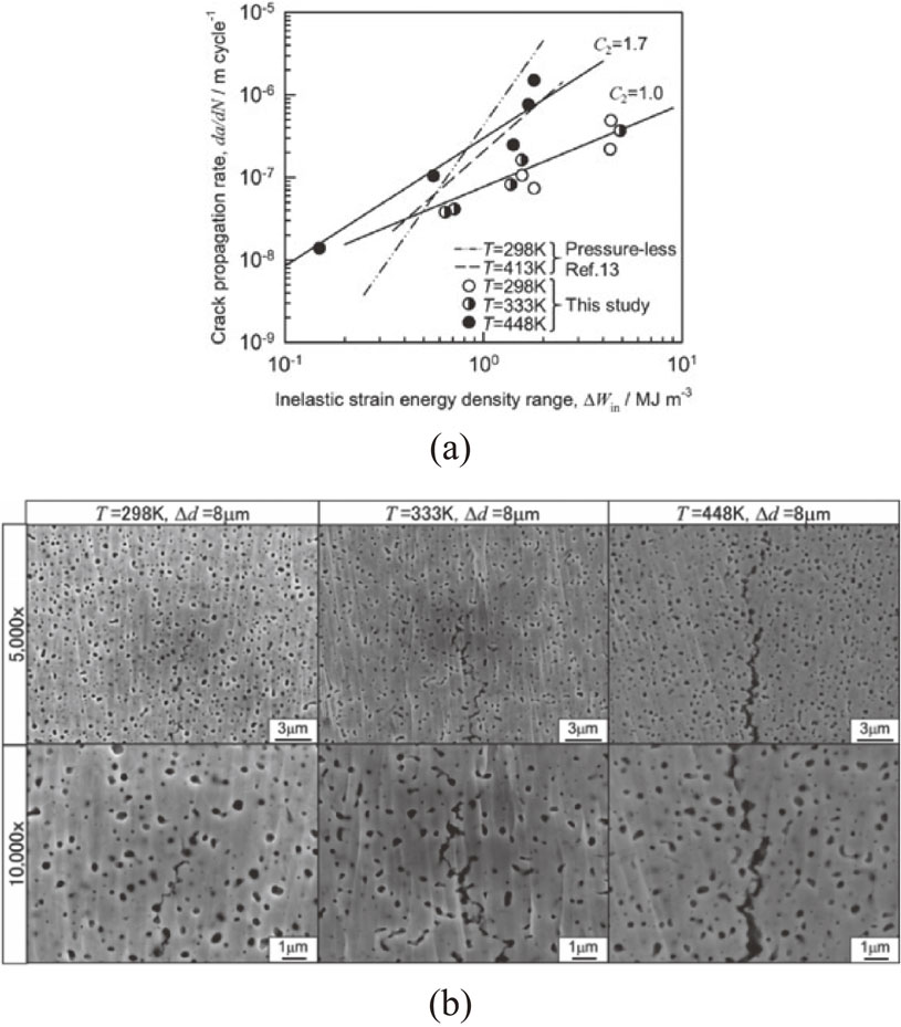
Fatigue crack propagation behavior of pressure-sintered Ag nanoparticles and its application to thermal fatigue life prediction. (a) Relationship between fatigue crack propagation rate of pressure-sintered Ag nanoparticles and ΔWin.25) “Ref. 13)” and “This study” in the legend correspond to the papers by Kimura et al.76) and Sato et al.,25) respectively. (b) SEM images showing microstructures around fatigue crack tip after fatigue test.
In addition to the sintered Ag materials, studies on low-cost sintered Cu materials with almost the same thermal and electrical conductivity as Ag have been conducted. Studies on the mechanical properties77) and joining reliability78,79) of sintered Cu materials have also been reported. The disadvantage of using Cu particles is that they can easily oxidize during joining. Consequently, researchers have proposed reducing the oxide film formed on Cu particles using an intense pulsed light (IPL) sintering process,80) a process in formic acid81,82) or H277,83) atmosphere, and using reducing solvents such as polyethylene glycol (PEG).84) Ag-coated Cu particles have also been proposed to prevent oxidation during high-temperature sintering.85)
Cu particles also have the problem of void formation due to the organics, as with Ag particles. To solve this problem, a solid-state joining technique using a nanoporous Cu sheet fabricated using dealloying has been developed.86) Interestingly, the nanoporous sheet can obtain high joining strength without using organic solvents. Many studies on the low-temperature process of sintered Cu materials have been reported. Cu nanoaggregates capable of low-temperature sintering have been developed.83,87) A large amount of Cu nanoaggregates, 5-nm in size is attached to the outer periphery of Cu particles protected by an organic layer. Due to the size effect, Cu nanoaggregates can improve the sintering properties at low-temperature and obtain a good joining state of the Cu–Cu joint. As for other methods, it has been reported that by sintering a mixture of copper particles and copper-based metal-organic decomposition ink, a highly conductive sintered copper film could be obtained at a sintering temperature of 100°C.88,89)
2.3 TLP materialsTLP joining is a method in which a low melting point metal reacts and joins with a high melting point metal by atomic diffusion and dissolution at a specific temperature. This process is similar to soldering; however, an intermetallic compound with a melting temperature higher than the process temperature is formed over the entire joint after joining. Therefore, it is possible to realize the multi-step joining of electronic components required to the manufacture power modules. Sn/Cu,90–96) Sn/Ni,95,96) Sn/Ag,97–99) In/Ag100) and In/Au100) have been reported as structures of TLP joint (interlayer/substrate or metallization). A combination of solder alloy/substrate such as Sn–Au/Cu,101,102) Sn–Au/Ni,103) Sn–Bi/Cu,104) Sn–Cu/Cu,105) and Sn–Ag/Cu106) has also been reported. In the case of Cu/Sn-based solder, there is a problem that voids are formed at the interface between the Sn-based solder and Cu substrate. The mechanism of void formation is due to imbalanced diffusion caused by the Kirkendall effect. It has been reported that a Zn layer is added to the joint interface to reduce Kirkendall voids.14) Figure 4 shows cross-sectional views of joint layer using deposited Sn/Cu/Zn/Sn coatings. By adding a thin Zn layer to the joint surface, the Zn segregation inhibits Cu diffusion and reduces the number of Kirkendall voids.

Cross sections of the joint interfaces using deposited Sn/Cu/Zn/Sn (= 2/0.38/0.02/2 µm thickness) coatings at 300°C with a bond time of 1800 s.14) (a) SEM image and (b) Zn mapping analysis result.
This process has the disadvantage of a long treatment time since TLP is diffusion joining. Therefore, to realize the formation of an intermetallic compound in the joint in a short time, a method for mixing Cu particles,107–109) Ag particles,110–112) Ni particles,113–115) In particles112,116) and Cu–Zn–Al particles104) with Sn-based solder powder or paste, and the application of Sn-coated Cu particles117) have been reported.
Another problem with the TLP joint is that hard and brittle intermetallic compounds are formed at the joints, making it difficult to withstand excessive thermal strain. Consequently, die-attach materials for power modules using TLP-polyimide resin composites have been developed118,119) to reduce the stiffness of the joints. The TLP joint structure, partially filled with polyimide resin, provides excellent thermal reliability. Another consideration is how to measure mechanical properties such as Young’s modulus, tensile strength and elongation of intermetallic compounds formed by the TLP joint. Methods for obtaining these mechanical properties include nanoindentation tests,120,121) bending tests101) using microcantilever manufactured by focused ion beams (FIB), and tensile tests using a TLP-joined at the center of the specimen.122)
Hereafter, we will focus on conductive materials such as aluminum and copper alloys for electronic material parts and their processing. Continuous advances in technology and engineering have made it possible to miniaturize machines, which require increased material strength and improved material workability. Alloying is one of the measures to increase strength. It was reported that Cu–Ni–Si alloy with the addition of Co and P has high strength due to the discontinuous precipitation after aging treatment123) and that Cu–Ti alloy with the addition of Mg has higher strength and elongation than Cu–Ti alloy.124) Also, the treatment of cold-sprayed pure Al substrate and Cu-clad Al wire causes mutual diffusion forming a reaction layer and increasing the strength.23,125) Furthermore, intermetallic compound layers formed on the Cu-clad Al wire are kinetically considered from the experimental and the analysis results.126)
Another way of improving mechanical properties is grain refining. In conventional manufacturing processes, solidification conditions’ effect on pure Cu castings was investigated, and because of the solidification conditions affecting the microstructure, it was shown that the deformation behavior was affected.127) Grain refinement using ultrasonic radiation during the casting of high-purity Al has been reported.128) Recently, ultrafine-grained structures produced by accumulative roll bonding (ARB) have attracted attention for improving material properties such as the ultimate tensile strength of processed high-purity Al, which increased 3–5 times compared with that of coarse-grained Al.129) It was also shown that the ultrafine-grained structure formed by equal-channel angular pressing (ECAP) could be simulated.130) By applying a miniaturized Charpy impact test to evaluate the toughness of small Cu and Al samples, it was confirmed that high reproducibility was obtained.22)
This study introduced current research on materials used in electronics, emphasizing on joining materials such as high-temperature lead-free solders, sintered and TLP materials, and conductive materials such as wiring and contact materials. The development of materials used in the electronics field, such as high-temperature joining and conductive materials, is advancing, and some of these materials are adopted in actual products. In the future, as products become more sophisticated, the elements required for materials will increase. For high-temperature joining materials, it is essential to achieve excellent thermal conductivity, mechanical and thermal fatigue properties while decreasing the joining temperature and time. For conductive materials, the material’s microstructure needs to be highly controlled to improve its mechanical properties and workability. To solve these problems and obtain high reliability, it is essential to understand the main causes of these phenomena, and it is necessary to continue studies in the future.