Materials Processing
Microstructural Change during Heat Exposure in Air of Modeled Environmental Barrier Coating Processed by Aerosol Deposition Method
2022 年 63 巻 11 号 p. 1567-1575

詳細
2022 年 63 巻 11 号 p. 1567-1575
Optimal deposition parameters for the aerosol deposition of a β-SiAlON coating and the microstructure change of an EBC after heat exposure in air are investigated. Dense and crystalline SiAlON coating having developed texture, where the (0001) plane is declined approximately 10° from the coating plane is formed. The deposition rate increases with the gas flow rate when the rate is ranging from 12 to 16 L/min. Further increase of the gas flow rate decreases the deposition rate. Regarding the 15 µm thick mullite coating deposited on SiAlON substrate heat exposed at 1573 K over 30 h, delamination of the coating occurs due to the oxidation of SiAlON. 30 µm thick mullite coating prevents the oxidation. As for the EBC deposited on Si–SiC substrate, delamination occurs at Si–SiC/SiAlON interface by the oxidation of SiC during heat exposure at 1573 K. At the bonded region during heat exposure, SiAlON prevents the mullite coating to become (SiO2+mullite) two-phase state by supping Al to the mullite. Residual Si at the substrate moves to SiAlON and mullite coating under heat exposure at 1673 K. Structure of EBC is maintained by using SiC substrate in which the Si will not move to the coating during exposure.
This Paper was Originally Published in Japanese in J. Japan Thermal Spray Soc. 57 (2020) 88–96.

Fig. 11 SEM micrographs and EDX maps showing a cross-section of a modeled EBC deposited on a SiC substrate. EDX maps showing the distribution of the Si, Al, O and N elements. The distribution of the elements is represented by shading. The as-deposited EBC specimens (a), (b) were heat exposed in air at 1673 K for (c), (d) 10 h.
In the jet engines of aircraft, further weight reduction of components and improvement of the combustion efficiency are required to reduce the environmental burden. The application of SiC fiber-reinforced SiC matrix (SiC/SiC) composites as high-temperature components for high-pressure turbines is being investigated because they are lightweight and have excellent heat resistance. It has been reported that SiC exhibits excellent oxidation resistance due to the formation of a SiO2 film on the surface of SiC under relatively high oxygen partial pressure.1,2) On the other hand, it is known that the assumed environment of use is a high-combustion environment that contains O2, CO2, and water vapor; therefore, the SiC is reduced due to the volatilization of oxides and hydroxides from SiC.3,4) The application of multi-layered environmental barrier coatings (EBCs) composed of a material such as mullite with excellent oxygen-shielding properties is thus indispensable. In recent years, a three-layer structure that uses Si as a bond coat layer, mullite, which is a compound of Al2O3 and SiO2 as an oxygen barrier layer, and rare earth (RE)-silicate as a water vapor barrier layer, has been proposed.5–7)
Conventional EBCs have been deposited by the atmospheric plasma spraying (APS) method. The mullite coating produced by the APS method has been reported to contain many amorphous phases because the molten high temperature mullite particles are rapidly cooled when the particles collide with the substrate.8) When an EBC in such a state is used in a high-temperature environment, the amorphous phased mullite crystallizes and cracks occur in the mullite coating due to shrinkage of the structure volume. Therefore, a method has been proposed in which the temperature of the substrate is kept above 1273 K and mullite is crystallized during the deposition process by the APS method.8) Even in this case, a porous coating forms; similar to the coating produced by the general APS method, so that the coating shrinks due to sintering when in a high-temperature environment. Tensile stress is generated in the direction parallel to the interface, which causes vertical cracks to occur in the coating. Such damage to the coating has become a problem because it leads to a decrease in the environmental shielding performance and delamination of the coating.6,7,9,10)
The aerosol deposition (AD) method is known to produce dense and crystalline coatings at room temperature.11–15) The ability to form a coating to a thickness of several tens of micrometers without heating is one advantage of the AD method. Various powders such as ZrO2,16–19) α-Al2O3,12,13,20–25) lead zirconate titanate (PZT)26,27) and AlN13) have been employed for AD coating to date. Therefore, it has been considered that mullite, which is a constituent material of EBCs, could also be formed by the AD method. In addition, it has been considered that a mullite coating could be formed that is stable even when used in a high-temperature environment. However, when a dense mullite coating is formed on a Si substrate by the AD method, Al in the mullite diffuses to the surface of the mullite coating in a high-temperature environment, and Si diffuses from the Si substrate into the mullite coating. As a result, a reacted layer is formed at the center of the coating and in the vicinity of the interface between the substrate and the coating, and the coating becomes a two-phase mixture of SiO2 and mullite that contains about 80% of SiO2.28) This phenomenon occurs when the surface of the mullite coating is exposed to high oxygen partial pressure and the vicinity of the interface between the Si substrate and the mullite coating is exposed to low oxygen partial pressure. Under such an oxygen partial pressure gradient, Al in the mullite diffuses from the low oxygen partial pressure side to the high oxygen partial pressure side, and the Al component is depleted in the mullite coating on the bond coat layer side, so that the mullite layer decomposes.29) SiAlON has attracted attention in recent years as a new bond coat layer to supply depleted Al and stabilize the structure of the mullite layer.30–32) In this study, the conditions for the deposition of SiAlON particles by the AD method were established. In addition, the modeled EBC specimen on which mullite and SiAlON are deposited was exposed to heat in the air, and the effect of heat exposure on the EBC microstructure was experimentally investigated.
The raw material powders used in this work were high purity mullite (Al6O13Si2; KM101, KCM Corporation Co., Ltd.) and β-SiAlON (Si3Al3O3N5; BSI3-001B(SN), AG Materials Inc.). The composition of the mullite powder was almost the same as the stoichiometric composition of mullite (Al2O3 71.9 mass%; impurities: Fe2O3 0.013, TiO2 0.004, CaO 0.008, MgO 0.012, Na2O 0.012, K2O 0.008, and ZrO2 0.001 mass%). The median diameter (D50) of the powder particles was 1.63 µm. Although the shape of the particles was slightly angular, it was almost equiaxed.28) The chemical composition of SiAlON powder was Si 29.8, Al 27.6, O 17.7, N 22.9, Fe 0.034, Ti 0.003, and Y 0.004 mass%. There was dispersion in particle size, and the median particle diameter was 1.04 µm (Fig. 1). All powders were sieved with a #60 sieve to remove large aggregates of powder. The powder was dried at 523 K before use. A SiAlON substrate (sintered body using Si3Al3O3N5 powder manufactured by AG Materials Inc.) was used to confirm the possibility of forming a mullite coating on SiAlON. In addition, a reaction sintered SiC (Si–SiC) substrate (Covalent Material Co., Ltd.) and a SiC substrate (ADMAP Inc., deposited on the Si surface of a single-crystal) were used to produce modeled EBCs.
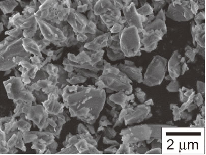
SEM micrograph of β-SiAlON raw powders used for the AD coating process.
The coating was deposited using an AD apparatus (Type GD-AE04/SS2, Fuchita Nanotechnology, Ltd.). The substrate temperature, carrier gas, and gas flow rate for deposition of the mullite coating were 353 K, He, and 28 L/min, respectively. The substrate temperature, carrier gas, and gas flow rate for deposition of the SiAlON coating were 303∼373 K, N2, and 12∼24 L/min, respectively. The dimensions (width and thickness) of the nozzle port were 20 × 0.5 mm or 30 × 0.5 mm for the deposition of all particles. During the deposition process, other parameters such as angle formed by the gas flow from the nozzle and the substrate surface (nozzle angle), nozzle-substrate distance, scan speed and number of scans were 60°, 3 mm, 50∼300 mm/min, and 20∼36 times, respectively.
2.2 Microstructure and textureThe thickness of the deposited coating was measured with a surface roughness meter (ET200, Kosaka Laboratory Ltd.). The texture of the SiAlON coating was characterized using the Schultz reflection method, with Cu Kα radiation filtered by a monochromator (Ultima IV, Rigaku Co.; 40 kV X-ray tube voltage and 40 mA tube current). A Si substrate was used for the measurement to prevent overlap between the SiAlON diffraction peaks and those from the substrate. From the incomplete pole figures obtained, the orientation distribution function (ODF) was calculated by the arbitrarily defined cell method33) (LaboTex Version 3.0.24, LaboSoft s. c.). The main component and sharpness of the texture were determined from the normalized pole figure and the inverse pole figure derived from the ODF.
The specimens were heat exposed in air at 1573 K for 10, 30, 50, and 100 h, and at 1673 K for 1 and 10 h. In addition, some specimens were heat-treated under a N2 gas atmosphere at 1573 K for 10, 30, and 50 h. The microstructure from the surface and cross-section of the coating specimens before and after heat exposure was observed using scanning electron microscopy (SEM; JSM-7001F, JEOL Ltd.; SU8010, Hitachi High-Technologies Corp.). Chemical composition analysis was performed using energy dispersive X-ray spectroscopy (EDX; TEAMTM EDS System, EDAX Inc.). In some specimens, the cross-section before observation was prepared using ion milling (IM4000 PLUS, Hitachi High-Technologies Corp.).
Figure 2 shows the effect of the gas flow rate on the deposition rate of SiAlON powder. Deposition was performed with the 20 mm wide nozzle. The substrate temperature, scan speed, and number of scans for the deposition were 303 K, 150 mm/min, and 20 times, respectively. The deposition rate increased with the gas flow rate up to 16 L/min and then decreased with further increase of the gas flow rate. Partial delamination of the coating was observed for the coating deposited at the highest gas flow rate. The relationship between the gas flow rate and the deposition rate by the AD method has been reported for TiN34) and Al2O325) powder at a nozzle angle of 90°, and for mullite powder28) at a nozzle angle of 60°. For both nozzle angles, the deposition rate increased with the gas flow rate up to a maximum value and then decreased. It is considered that deposition of the coating occurs due to the fracture and plastic deformation of particles at the time of collision with the substrate, which is referred to as the room temperature impact consolidation phenomenon.12,13) Therefore, when the gas flow rate is low, the particles cannot obtain the critical velocity at which the coating will form, and no coating will be formed on the substrate. When many particles exceed the critical velocity to form a coating, then a coating will be deposited and the deposition rate increases. However, when the gas flow rate is too high, the deposition rate decreases due to the occurrence of wear by the collision of the particles with the coating surface due to the increase in the velocity of the particles.34) The same phenomenon occurred during the formation of SiAlON powder coatings, and the relationship between the deposition rate and the gas flow rate shown in Fig. 2 was obtained.

Relationship between deposition rate and gas flow rate.
Figure 3 shows the surface and cross-sectional microstructure of the SiAlON coating deposited at a gas flow rate of 12 L/min. Although no cracks or chips were observed on the surface of the coating, a flat-shaped region was observed on a part of the coating surface as if the particles were crushed by collision (Fig. 3(a)). The formation of such a region is considered to be due to plastic deformation caused by particle collision with the substrate during deposition. The formation of a dense coating was revealed by cross-sectional microstructure observations of the coating; no voids were observed at this magnification (Fig. 3(b)). Figure 4 shows a (0001) pole figure of the deposited SiAlON coating. The deposition was performed with the 30 mm wide nozzle, a substrate temperature of 373 K, a gas flow rate of 19 L/min, a scan speed of 300 mm/min, and 36 scans. A fiber texture in which the (0001) plane was tilted approximately 10° from the deposition plane was observed. The maximum pole density was approximately 10, which indicates that the texture is developed. Here, the random level is 1.
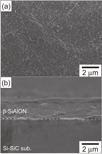
SEM micrographs of a β-SiAlON coating deposited on reaction-sintered Silicon Carbide (Si–SiC) substrate: (a) surface of as-deposited specimen, and (b) cross-section of as-deposited specimen.
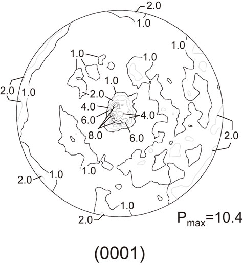
(0001) pole figure of β-SiAlON coating deposited on Si substrate.
Figure 5 shows the cross-sectional microstructure and EDX elemental analysis results for a part of the cross-sectional area of a specimen after heat exposure at 1573 K for various times. The distribution of elements is represented by shading, where bright regions indicate the presence of many elements, and dark regions indicate the presence of few elements. The thickness of the coating was about 15 µm. Fine voids were observed in the cross-section of the coating, regardless of the thickness direction of the coating, although the coating was mostly dense (Fig. 5(a)). The cross-sectional elemental mapping indicated that Si, Al and O were evenly distributed throughout the coating (Fig. 5(b)). The formation of the voids was observed for the heat exposure at 1573 K for 10 h. However, no delamination of the coating was observed (Fig. 5(c) and (d)). Delamination was observed for heat exposure at 1573 K for 30 h (Fig. 5(e)). Elemental analysis of the delaminated part suggested that the delamination occurred at the interface between the mullite and SiAlON (Fig. 5(f) and (g)). However, as shown in the heat exposed mullite coating deposited on a Si substrate, diffusion of Al to the mullite coating surface or diffusion of Si into the mullite coating from the Si substrate were not observed.28)
SEM micrographs and EDX maps showing a cross-section of a 15 µm thick mullite coating deposited on a β-SiAlON substrate. EDX maps showing the distribution of the Si, Al and O elements. The distribution of the elements is represented by shading. Bright regions indicate the presence of many elements. The as-deposited specimens (a), (b) were heat exposed in air at 1573 K for (c), (d) 10, and (e), (f), (g) 30 h.
There are two possible reasons for interfacial delamination. One is delamination due to thermal stress caused by the difference in thermal expansion coefficient between mullite and SiAlON due to the increase in temperature. The other is delamination due to the oxidation of SiAlON. Assuming the thermal stresses generated in the direction parallel to the interface between the substrate and each coating layer are σs and σi, respectively, the thermal stress applied to the substrate and each layer in the case of a specimen having n layers of coating on the substrate will be given based on the report by Hsueh:35)
| \begin{equation} \sigma_{s} = E_{s}\left(c + \frac{z - t_{b}}{r} - \alpha_{s}\varDelta T \right)\quad (- t_{s} \leq z \leq 0) \end{equation} | (1) |
| \begin{equation} \sigma_{i} = E_{i}\left(c + \frac{z - t_{b}}{r} - \alpha_{i}\varDelta T \right)\quad (i = 1 - n), \end{equation} | (2) |
| \begin{equation} c = \frac{\left(E_{s}t_{s}\alpha_{s} + \displaystyle\sum\nolimits_{i = 1}^{n}E_{i}t_{i}\alpha_{i} \right)\varDelta T}{E_{s}t_{s} + \displaystyle\sum\nolimits_{i = 1}^{n}E_{i}t_{i}} \end{equation} | (3) |
| \begin{equation} t_{b} = \frac{- E_{s}t_{s}^{2} + \displaystyle\sum\nolimits_{i = 1}^{n}E_{i}t_{i}(2h_{i - 1} + t_{i})}{2\left[E_{s}t_{s} + \displaystyle\sum\nolimits_{i = 1}^{n}E_{i}t_{i} \right]} \end{equation} | (4) |
| \begin{equation} \frac{1}{r} = \frac{3\left[E_{s}(c - \alpha_{s}\varDelta T)t_{s}^{2} - \displaystyle\sum\nolimits_{i = 1}^{n}E_{i}(c - \alpha_{i}\varDelta T)t_{i}(2h_{i - 1} + t_{i}) \right]}{E_{s}t_{s}^{2}(2t_{s} + 3t_{b}) + \displaystyle\sum\nolimits_{i = 1}^{n}E_{i}t_{i}[6h_{i - 1}^{2} + 6h_{i - 1}t_{i} + 2t_{i}^{2} - 3t_{b}(2h_{i - 1} + t_{i})]}, \end{equation} | (5) |
| \begin{align} &\text{4(Si$_{3}$Al$_{3}$O$_{3}$N$_{5}$) (s)} + \text{15O$_{2}$ (g)} \\ &\quad\rightarrow \text{2(3Al$_{2}$O$_{3}{\cdot}$2SiO$_{2}$) (s)} + \text{8SiO$_{2}$ (s)} + \text{10N$_{2}$ (g)}. \end{align} | (6) |
| \begin{align} \text{$\beta$-SiAlON (s)} &\rightarrow \text{15R-SiAlON (s)} + \text{4SiO (g)}\\ &\quad +\text{2N$_{2}$ (g)} + \text{Si (l)} \end{align} | (7) |
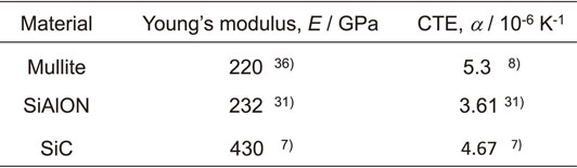
Figure 6 shows the cross-sectional microstructure and the results of EDX elemental analysis of a partial area of the cross-sectional microstructure. The specimen with a 15 µm thick mullite coating was heat treated at 1573 K for 50 h in N2 gas and that with a 30 µm thick mullite coating was heat exposed at 1573 K for 100 h in the air. The distribution of the amount of the elements is represented by shading, where bright regions indicate the higher concentration of each element and dark regions indicate the lower concentration of each element. No interfacial delamination was observed when the heat treatment was performed in N2 gas (Fig. 6(a) and (b)). When the delamination of coating and substrate is due to thermal stress, it will occur even when heating in N2 gas. However, no delamination was observed, even if the specimen was held at 1573 K for 50 h. Therefore, the delamination by heat exposure in the air is mainly due to the generation of N2 gas by the oxidation of SiAlON. However, it is also considered that delamination occurs due to the force induced by the bulging of the coating accompanied by the formation of bubbles from the generation of gas, and the force caused by buckling of the coating due to the compressive load applied to the coating. When the mullite coating thickness was doubled to about 30 µm and exposed to heat in the air at 1573 K for 100 h, no delamination of the coating was observed over a wide range of the specimen (Fig. 6(c)–(e)). It was thus clarified that the oxidation of SiAlON can be suppressed with a thickness of about 30 µm if the mullite coating is dense. It was also determined that the coating does not delaminate if the oxidation of SiAlON can be suppressed.
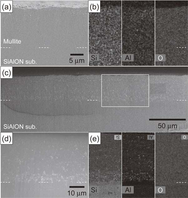
SEM micrographs and EDX maps showing a cross-section of a mullite coating deposited on a β-SiAlON substrate. EDX maps showing the distribution of the Si, Al and O elements. The distribution of the elements is represented by shading. The specimen having 15 µm thick mullite coating was heat treated in N2 gas at 1573 K for 50 h (a), (b). The specimen having 30 µm thick mullite coating was heat exposed in air at 1573 K for 100 h (c), (d), (e).
In the mullite coating on the SiAlON substrate, the formation of a reacted layer containing SiO2 as the main component was not observed. The reacted layer that forms at the mullite coating on the Si substrate is due to the diffusion of Al to the mullite coating surface from the inside of mullite and the diffusion of Si into the mullite coating from the Si substrate. It is difficult to suppress the diffusion of Al to the surface of the mullite coating because of the oxygen partial pressure gradient. However, it is considered that the mullite coating was maintained by the supply of Al from SiAlON. In addition, the inclusion of N in SiAlON is expected to suppress the formation of SiO2 (cristobalite) because the crystal structure is maintained even if Al is depleted in SiAlON. It was clarified that the decomposition of dense mullite can be suppressed by changing the bond coat layer from Si to SiAlON. Based on these results, modeled EBCs with about 4 µm thick SiAlON and about 50 µm thick mullite was deposited on the reaction-sintered SiC (Si–SiC) and SiC substrates, and the effect of microstructural change on the modeled EBCs was examined by heat exposure in air.
3.3 Microstructure of modeled EBC under heat exposure in airFigure 7 shows the cross-sectional microstructure of the modeled EBC specimen deposited on the Si–SiC substrate that was heat exposed in the air at 1573 K for various times. Delamination between the coating and the substrate was observed partially in the specimen that was heat exposed in the air at 30 h (Fig. 7(a)). The number of delaminated regions increased with the heat exposure time for 50 h and 100 h, and small delaminations were observed ahead of the delamination front, as shown by the arrows (Fig. 7(b) and (c)). EDX elemental analysis was performed to evaluate the changes in the microstructure of the coating in the delaminated and non-delaminated areas. Figure 8 shows the cross-sectional microstructures of the as-deposited modeled EBC specimen and specimens exposed to heat at 1573 K in air for various times. The elemental analyses were performed for the areas indicated by the white lines. The distribution of the amount of the elements is represented by shading, where bright regions indicate the higher concentration of each element and dark regions indicate the lower concentration of each element. The thickness of the mullite coating was about 50 µm. Fine voids were observed, although it is generally considered a dense coating (Fig. 8(a)). EDX elemental mapping in the vicinity of the interface between the substrate and coating revealed Si, Al, O, and N were uniformly distributed throughout each coating. The Si–SiC substrate, SiAlON layer, and mullite layer could be identified according to the composition. The thickness of the SiAlON layer was about 4 µm (Fig. 8(b)). The elemental analysis revealed that the delaminated region was at the interface between the Si–SiC substrate and SiAlON layer for the specimen after heat exposure in the air at 30 h (Fig. 8(c) and (d)). The boundary between the SiAlON layer and the mullite layer, which remained joined even after 30 h heat exposure in air, became indistinguishable from the results of the elemental analysis. The concentration of Al was high on the surface side of the mullite layer, and low on the mullite side and SiAlON layer of the interface between the SiAlON layer and the mullite layer (Fig. 8(e) and (f)). Furthermore, as the heat exposure time was increased to 50 and 100 h, the region of the mullite layer with low Al concentration expanded toward the surface of the mullite layer. However, as in the case of the mullite coating on the Si substrate, the Si composition did not increase in the region of low Al content, which suggests that the reaction layer does not form in this region (Fig. 8(g)–(j)). Although the Al in the mullite layer diffuses to the surface of the mullite layer due to the oxygen partial pressure gradient, the formation of the reacted layer at the mullite layer is considered to be suppressed by the supply of Al from the SiAlON layer to the mullite layer.29,30,32) In addition, the boundary between the SiAlON layer and the mullite layer is indistinguishable; therefore, there is a possibility that the SiAlON layer changes to the mullite layer due to oxidation, as shown in eq. (6), under low oxygen partial pressure caused by oxide ions from the mullite layer.

SEM micrographs showing a cross-section of a modeled EBC deposited on a reaction-sintered Silicon Carbide (Si–SiC) substrate. The specimens were heat exposed in air at 1573 K for (a) 30, (b) 50, and (c) 100 h.
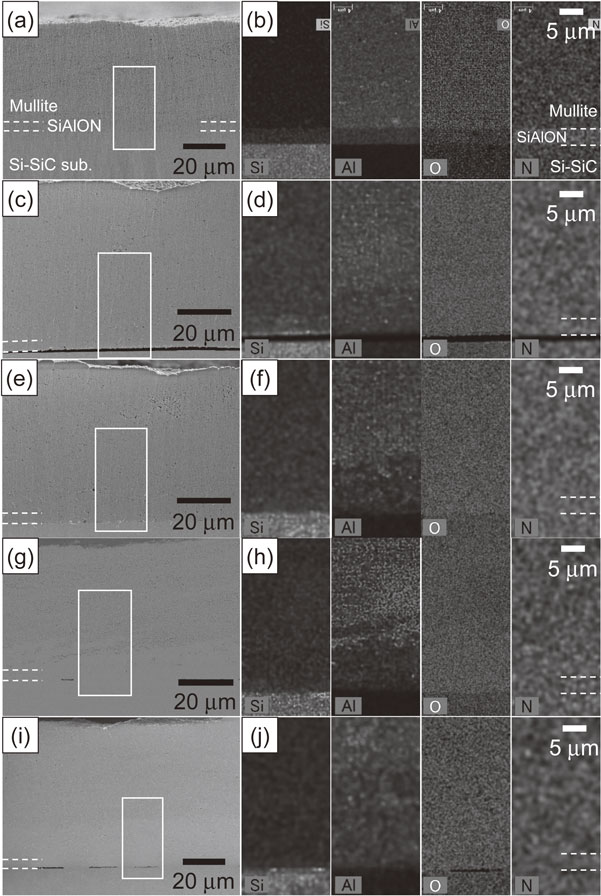
SEM micrographs and EDX maps showing a cross-section of a modeled EBC deposited on a Si–SiC substrate. EDX maps showing the distribution of the Si, Al, O and N elements. The distribution of the elements is represented by shading. The as-deposited EBC specimens (a), (b) were heat exposed in air at 1573 K for (c), (d), (e), (f) 30, (g), (h) 50, and (i), (j) 100 h.
Two reasons are considered for the delamination at the interface between the Si–SiC substrate and SiAlON layer. One is delamination due to the thermal stress caused by the difference in the thermal expansion coefficients of Si–SiC, SiAlON, and mullite during heating. The other reason is the oxidation of SiC. In the former case, thermal stress in the vicinity of the interface of the Si–SiC substrate, SiAlON layer, and mullite layer can be derived by applying Young’s moduli and the thermal expansion coefficients shown in Table 1, and thickness of the substrate and each layer to eqs. (1) to (5) in the case i = 2. Thermal stresses in the vicinity of the interface of the Si–SiC substrate, SiAlON layer, and mullite layer were thus 9.9 MPa, 318 MPa, and −171 MPa, respectively. Compressive and tensile loads are applied to the mullite layer and SiAlON layer, respectively; therefore, delamination could occur at the interface between mullite and SiAlON due to buckling of the mullite layer. However, the thickness of the SiAlON layer (4 µm) is thinner than that of the mullite layer (50 µm), so that the SiAlON layer could also delaminate due to buckling when the mullite and SiAlON layers are strictly bonded. Even if thermal stress occurs, considering that the SiAlON layer has changed to a mullite layer due to oxidation, the mullite layer is still subject to a compressive load, and the possibility of delamination due to buckling remains. On the other hand, when considering the oxidation of SiC, the SiAlON layer and the mullite layer are in contact with the SiC; therefore, it is considered to be active oxidation under low oxygen partial pressure and the formation of SiO and CO gas are reported as:1,2)
| \begin{equation} \text{SiC (s)} + \text{O$_{2}$ (g)} \rightarrow \text{SiO (g)} + \text{CO (g)}. \end{equation} | (8) |
Figure 9 shows the cross-sectional microstructure of the modeled EBC specimen heat-treated at 1573 K for 50 h in N2 gas. Large-scale delamination of the coating was not observed macroscopically (Fig. 9(a)). Delamination on a small scale was also not confirmed in the microscopic region (Fig. 9(b)). If interfacial delamination occurs between the coating and the substrate due to the thermal stress, then delamination would occur even when the specimen is heated in N2 gas. However, no delamination was observed even after holding for 50 h; therefore, any delamination would be caused by the generation of SiO and CO gas due to the oxidation of SiC.

SEM micrographs of a modeled EBC deposited on a Si–SiC substrate. The specimens were heat treated in N2 gas at 1573 K for 50 h. Cross-section view of (a) low magnification and (b) high magnification.
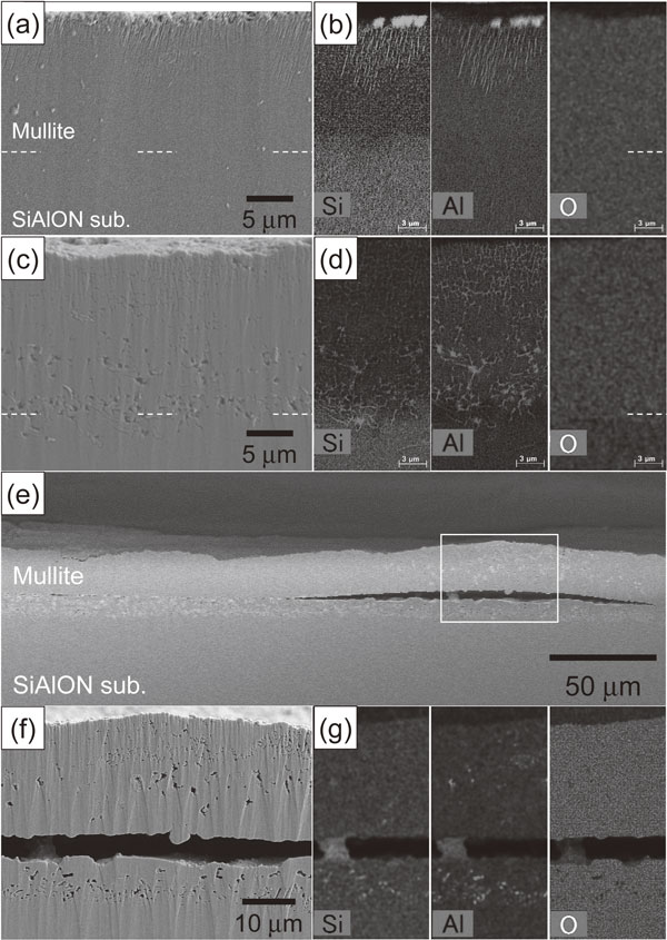
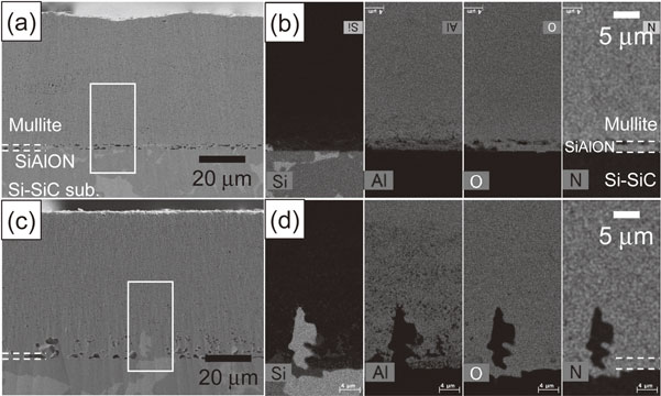
SiAlON has higher heat resistance than Si; therefore, it is considered for use as the bond coat for EBCs applied at 1673 K.31,32) The modeled EBC with Si–SiC as a substrate was thus exposed to heat at 1673 K for up to 10 h. Figure 10 shows the cross-sectional microstructures of the modeled EBC specimens exposed to heat at 1673 K in air for 1 and 10 h. EDX elemental analyses were performed for the areas indicated by the white lines. The distribution of the amount of the elements is represented by shading, where bright regions indicate the higher concentration of each element and dark regions indicate the lower concentration of each element. After heat exposure in air, relatively large voids were observed at the interface between the Si–SiC substrate and the SiAlON layer, and in the vicinity of the interface between the mullite and SiAlON layers (Fig. 10(a)). The concentration of the Al in the mullite layer in the vicinity of the interface between the SiAlON layer and the mullite layer, and in the SiAlON layer tended to be low compared to the central part of the mullite layer (Fig. 10(b)). When the specimen was heat exposed in air for 10 h, the size of the voids observed along the interface became slightly larger, and appeared to spread toward the surface of the mullite layer. The bright shade phases present in the Si–SiC substrate were partially in the SiAlON layer and in the mullite layer (Fig. 10(c)). Chemical analysis revealed that the bright phase was Si. In addition, the concentration of Al tended to be low near up to the central part of the mullite layer (Fig. 10(d)). It was thus clarified that there is a problem in that some residual Si in the Si–SiC substrate moves to the SiAlON and mullite layers at 1673 K. Figure 11 shows the cross-sectional microstructures of the as-deposited modeled EBC where the substrate has changed from Si–SiC to SiC and the EBC was exposed to heat at 1573 K in air for 10 h. EDX elemental analyses were performed for the areas indicated by the white lines. The distribution of the amount of the elements is represented by shading, where bright regions indicate the higher concentration of each element and dark regions indicate the lower concentration of each element. Almost dense coatings were formed (Fig. 11(a)). EDX elemental mapping distinguished the SiC substrate, SiAlON layer, and mullite layer according to the composition (Fig. 11(b)). As in the case of the EBC with the Si–SiC substrate, many voids were observed at the interface (Fig. 11(c)), and the concentration of Al tended to be low near up to the central part of the mullite layer (Fig. 11(d)) after heat exposure in the air for 10 h. However, since Si is not included in the SiC substrate, the penetration of residual Si to the SiAlON and mullite coating layers will not occur as in the case of Si–SiC substrate. Therefore, when an EBC on a SiC/SiC composite is applied at 1673 K, the use of a composite substrate in which Si does not remain is required.
SEM micrographs and EDX maps showing a cross-section of a modeled EBC deposited on a Si–SiC substrate. EDX maps showing the distribution of the Si, Al, O and N elements. The distribution of the elements is represented by shading. The EBC specimens were heat exposed in air at 1673 K for (a), (b) 1, and (c), (d) 10 h.

SEM micrographs and EDX maps showing a cross-section of a modeled EBC deposited on a SiC substrate. EDX maps showing the distribution of the Si, Al, O and N elements. The distribution of the elements is represented by shading. The as-deposited EBC specimens (a), (b) were heat exposed in air at 1673 K for (c), (d) 10 h.
The process of β-SiAlON coating using the AD method and the microstructural changes of the modeled EBC specimens due to heat exposure in the air, were experimentally investigated. The major conclusions are summarized as follows:
This research was supported by the Council for Science, Technology, and Innovation (CSTI), Cross-ministerial Strategic Innovation Promotion Program (SIP), and “Structural Materials for Innovation” (Funding agency: Japan Science and Technology Agency (JST)). Furthermore, this research was supported by a grant-in-aid for scientific research (B) (18H01745) from the Japan Society for the Promotion of Science. The authors greatly appreciate the grants. The authors express their gratitude to Mr. T. Kayama and Mr. K. Sagawa for their contributions to the experiments.