抄録
Multilayer iron-doped indium-saving indium–tin oxide (ML ITO50:Fe2O3) thin films with high conductivity and high transmittance in the visible spectrum have been fabricated by sputtering method. Structures consisting of very thin layer of conventional indium tin oxide (90 mass% In2O3–10 mass% SnO2) and iron-doped indium-saving indium–tin oxide layer with reduced content of In2O3 (ITO50:Fe2O3) to 50 mass% are discussed. By optimizing oxygen flow rate in iron-doped indium-saving indium–tin oxide layer, the lowest volume resistivity of 3.78 × 10⁻⁴ Ω·cm, mobility of 29.8 cm2/(V·s), carrier concentration of 4.60 × 1020 cm−3 and transmittance larger than 90% in the visible range have been achieved. ML ITO50:Fe2O3 thin films deposited under optimal conditions demonstrated lower volume resistivity and higher transmittance than undoped multilayer indium-saving ITO thin films and iron-doped single-layer thin films obtained under the same oxygen flow rate Q(O2) = 0.1 sccm. ML ITO50:Fe2O3 thin films demonstrated optimal parameters at the lower oxygen flow rate (Q(O2) = 0.1 sccm) than undoped ML ITO50 thin films. ML ITO50:Fe2O3 thin films are crystallized and show In4Sn3O12 structure.
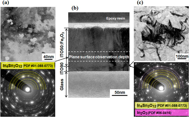
Fig. 3 TEM images of as-deposited ML ITO50:Fe
2O
3 thin film: (a) plane view image from 2nd layer, (b) cross-sectional image and (c) plane view image closed to interface between 1st and 2nd layers. SAED patterns of 2nd layer (a) and closed to interface between 1st and 2nd layers (c).
Fullsize Image

