1. Introduction
Heterophase metallic multilayer materials, composed of alternating layers of dissimilar metals with thicknesses ranging from several millimeters to a few nanometers, have garnered increasing interest as a new design approach for structural materials with improved mechanical properties compared to bulk single-phase materials.1,2) Traditional fabrication methods, such as electrodeposition or physical vapor deposition (PVD), allow precise control of layer thicknesses and crystal orientation relationships at interfaces, but are limited to producing materials in the form of thin films.3–6) Recent advances in severe plastic deformation (SPD) processes, particularly accumulative roll bonding (ARB), have enabled the fabrication of bulk nanolaminates, such as copper/niobium (Cu/Nb) nanolaminates, opening the door for their use as structural materials.6–8)
The effect of the ARB process on the layer thickness distribution, texture development, orientation relationship at interfaces and mechanical behavior of Cu/Nb composites has been extensively studied both experimentally,6–10) theoretically,11) and numerically.12–17) The strain accumulation during repeated rolling in the ARB process causes significant changes in texture for both the body-centered cubic (bcc) Nb phase and the face-centered cubic (fcc) Cu phase. The Nb phase tends to exhibit strong α-fiber and γ-fiber that are characteristic of rolled fcc crystals while the Cu phase shows a dominance of Copper {112}⟨111⟩ and Goss {110}⟨001⟩ components but with lower intensity than in the Nb phase.5,6) The strength of the fiber texture was observed to be highest at grains near Cu/Nb interfaces. The texture evolution with the ARB process is different from that of rolled single phase Cu and Nb which was inferred to be due to the Cu/Nb interface preventing dynamic recrystallization.5,6) Indeed, the continuous crystal reorientation due to the ARB process results in a specific orientation relationship at the Cu/Nb interface18) which was not observed in the cases of Al/Nb interfaces,19,20) although both are fcc/bcc nanolayers with similar initial microstructures. At the difference of the Kurdjumov-Sachs (KS) or Nishiyama-Wasserman (NW) orientation relationship, {111}Cu||{110}Nb, observed in PVD for the plane interface, the Cu/Nb interface in ARB composite is {112}Cu||{112}Nb2,5) and semi-coherent which was found to be metastable by crystal plasticity finite element (CPFE) simulation of bicrystal.12) The yield strength was found to be length-scale dependent, generally increasing monotonically with the decrease in the layer thickness, following a Hall-Petch type relationship, while the ductility showed the opposite trend.10) The Hall-Petch relationship was found to predict the strength for layer thickness as low as 5 nm.11) Other strengthening mechanisms such as the single-dislocation-based confined layer slip (CSL) model may be applied for lower thicknesses.21) Significant in-plane strength anisotropy between the rolling direction (RD) and the transverse direction (TD) was also reported and was argued to be due to the strong crystallographic texture based on visco-plastic self-consistent (VPSC) simulations.10)
To be suitable as structural materials, it is important to understand not only the deformation behavior but also the failure mechanisms under both monotonic and cyclic loading. In PVD Cu/Nb nanolaminates, decreasing the layer thickness resulted in a transition from brittle opening fracture to a more ductile shear mode, with a similar trend observed when decreasing the thickness of the Cu phase compared to the Nb phase, highlighting the ductile and brittle characteristics of each phase.22) A fracture toughness model that considered the effect of different layer thicknesses and used linear elastic fracture mechanics accurately predicted these observations.22) In-situ bending of micro-beam ARB Cu/Nb specimens along the RD and TD direction and containing a micro-notch revealed a strong anisotropy and orientation dependence of the interface shear strength and individual layer strengths on failure behavior.23,24) Molecular dynamics simulations confirmed that the Cu/Nb {112}Cu||{112}Nb interface of ARB samples does not shear in the RD while the shear strength along the TD was found to be about 1.2 GPa.25)
To the authors’ best knowledge, the fatigue behavior of ARB Cu/Nb materials have not been clarified yet. Thus, the objective of the present work is to investigate the effect of the loading direction on the tensile and fatigue behavior of a Cu/Nb laminates by means of experimental analyses and CPFE simulations.
2. Material and Method
2.1 Material
The material investigated was a Cu/Nb laminate procured from Takefu Special Steel Co. Ltd. (Japan) containing equal volume fraction of Cu and Nb and fabricated by ARB from pure Cu and Nb sheets. At first, Nb and Cu sheets were stacked and sealed within a container. It was then rolled to a 1 mm thickness plate, unsealed, and cut into smaller pieces. The process was repeated until obtaining a sheet containing 500 layers (250 Nb and 250 Cu). The material on the surface of the final sheet was always the Cu phase.
The final microstructure was examined by means of optical microscopy (OM) and electron backscatter diffraction (EBSD) measurement using a field emission scanning electron microscope (SEM, JEOL JSM-4700F) at an acceleration voltage of 20 kV.
Tensile tests were carried out on flat dog-bone specimens with the tensile axis aligned along either the RD or the TD. The gauge dimensions were 20 × 4 × 1 mm. The tests were performed on a servo-hydraulic machine under strain control, with a constant strain rate of 1.0 × 10⁻³ s−1. The strain was controlled and measured by a 5-mm clip-on extensometer.
Four-point bending fatigue tests were carried out on a micro-testing machine (SHIMADZU Micro-servo MMT-500N), with a stress ratio R = 0.1 and a frequency f = 20 Hz. Specimens with a rectangular cross section of 5 × 1 mm were machined with the tensile axis aligned either along the RD or TD. The loading span corresponded to 1/3 of the support span which was set to 30 mm. The fatigue tests were carried out until failure or until 107 cycles. A 45° inclined mirror was positioned below the specimen surface subjected to a tensile stress and a digital microscope was employed to observe the time of appearance of micro-cracks in-situ by interrupting the tests at regular cyclic intervals (1000 cycles in the present work). The tensile surface of the specimens was polished with a P4000 silicon carbide paper to reduce the initial surface roughness.
2.2 Crystal plasticity model
To clarify the effect of the loading direction on the local elasto-plastic response of the microstructure at the grain scale, crystal plasticity finite element simulations were carried out on synthetic microstructures. To this end, a phenomenological rate-dependent crystal plasticity model was employed. Assuming plastic deformation in both Cu and Nb phase is carried out by dislocation slip on Ns slip systems, the plastic velocity gradient is defined as:26,27)
| \begin{equation}
\boldsymbol{L}_{p} = \sum\nolimits_{\alpha=1}^{N_{s}} \dot{\gamma}_{0}\left| \frac{\tau^{\alpha}}{\tau_{c}^{\alpha}} \right|^{n}\mathit{sgn}(\tau^{\alpha})\boldsymbol{m}^{\alpha} \otimes \boldsymbol{n}^{\alpha},
\end{equation}
| (1) |
where $\dot{\gamma }_{0}$ is the reference shear rate taken as 10−3 s−1, n is the strain rate exponent, $\tau^{\alpha}$ is the resolved shear stress and $\tau_{c}^{\alpha }$ is the critical resolved shear stress (CRSS) on the slip system α of direction and normal vectors mα and nα, respectively. Twelve {110}⟨111⟩ and twelve {112}⟨111⟩ slip systems are considered for the bcc Nb phase while twelve {111}⟨110⟩ slip systems are active in fcc Cu. The evolution of the CRSS follows a Voce-type law:
| \begin{equation}
\tau_{c}^{\alpha} = \tau_{0}^{\alpha} + \tau_{1}^{\alpha} \left(1 - e^{-\frac{b_{1}^{\alpha}}{\tau_{1}^{\alpha}}\Gamma_{s}} \right),
\end{equation}
| (2) |
with
| \begin{equation}
\dot{\tau}_{c}^{\alpha} = \frac{d\tau_{c}^{\alpha}}{d \Gamma_{s}}\sum\nolimits_{\zeta = 1}^{N_{s}} h^{\alpha \zeta}|\dot{\gamma}_{s}^{\zeta}|.
\end{equation}
| (3) |
$\tau_{0}^{\alpha }$, $\tau_{0}^{\alpha } + \tau_{1}^{\alpha }$, $b_{1}^{\alpha }$ are the initial strength, the saturated strength and initial hardening rate of the slip system α, respectively. Γs is the total shear strain, hαζ is the interaction coefficient between the slip systems α and ζ, set to 1 for simplicity, and $\dot{\gamma }_{s}^{\zeta }$ the shear strain rate on the slip system ζ. The crystal plasticity model was implemented as a user-material (UMAT) for the FE software Abaqus following the forward gradient time integration scheme.
3. Results and Discussion
3.1 Microstructure analysis and modeling
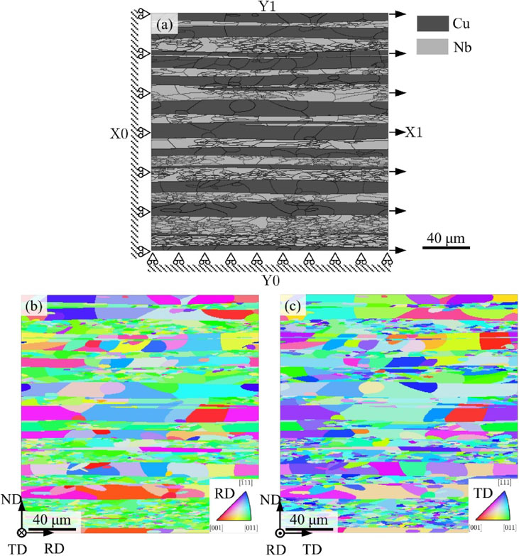
Figure 1(a)–(b) presents an EBSD map on the RD face, using inverse pole figure (IPF) color coding to distinguish the Cu and Nb phases. The layers were not entirely uniform, with individual layer thicknesses ranging from 1–2 µm to 30–40 µm for both phases, and each layer exhibiting some degree of waviness along the normal direction (ND). Table 1 provides the mean and standard deviation of layer thicknesses for each phase, which averaged around 6 µm. The grain shape is highlighted in the grain boundary misorientation map in Fig. 1(c). To characterize the grain morphology of each phase statistically, each grain was approximated with an ellipse having a major axis (a) and aspect ratio (b/a), using a misorientation angle of 5° as the threshold for identifying grains. Figure 1(d)–(g) displays the probability distributions of grain major axis size and aspect ratio for the two phases. The Cu phase had a relatively coarse microstructure, with an average grain major axis of 11 µm, elongated along the layer direction and a mean aspect ratio of 0.33. In contrast, the Nb phase exhibited a heavily refined grain structure, with an average grain major axis of approximately 3 µm and a mean aspect ratio of 0.2. Most grains in both phases were inclined parallel to the layer direction, and the coarse layers were composed of multiple grains stacked along the ND.
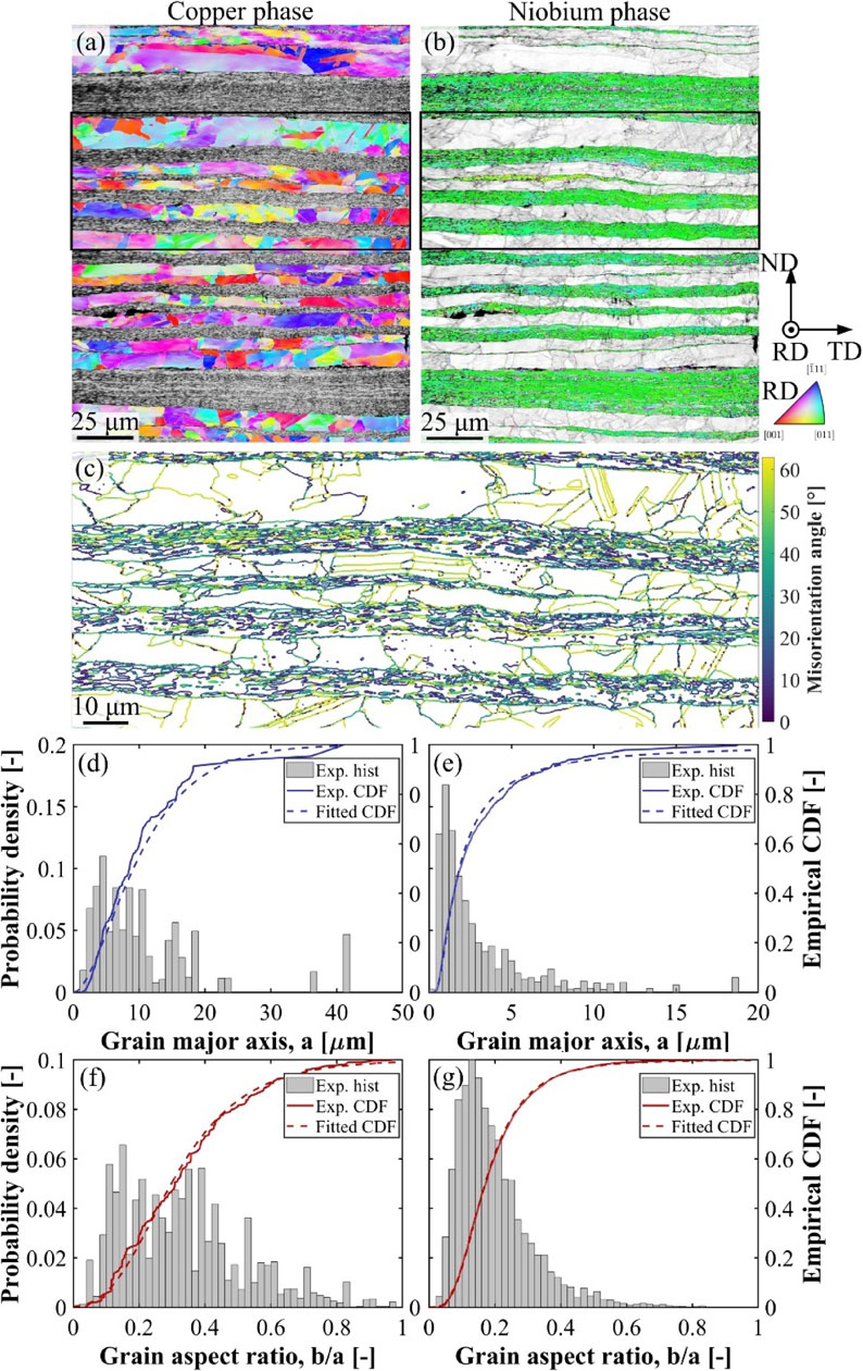
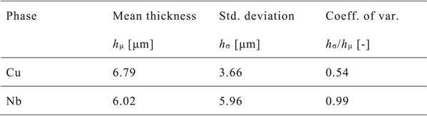
Table 1 Mean, standard deviation, and coefficient of variation of the thickness layers for the two phases.
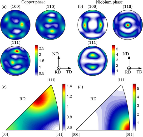
In Fig. 1(a), the IPF map of the Cu phase revealed local variations in crystal orientation within each grain, indicating high retained plastic strain. Additionally, multiple {111}⟨112⟩ twins were observed. In contrast, the Nb phase showed a nearly uniform orientation map, with most grains having one of their ⟨110⟩ directions parallel to the RD. The orientation distribution functions (ODFs) for the Cu and Nb phases are presented on the {100}, {110}, and {111} pole figures, as well as on the IPF along the RD, in Fig. 2. The Cu phase exhibited a weak texture, with a maximum index value close to 2.5. A weak Brass orientation {110}⟨1-12⟩ was also observed on the IPF in Fig. 2(c). In contrast, the Nb phase showed almost a single crystal texture, with a peak texture index value above 5 localized on the {110} pole figure near the RD. This orientation corresponds to an α-fiber texture (⟨110⟩||RD), as confirmed by the IPF in Fig. 2(d). A weak γ-fiber texture (⟨111⟩||ND) was also present. These results are consistent with previous studies by Carpenter et al.,5) which extensively analyzed the texture evolution of the two phases as a function of layer thickness. The study showed that as the layer thickness decreased, the Nb phase tended to continuously evolve towards a single orientation component, while multiple orientations were still observable in the Cu phase at all length scales.
The EBSD measurement data was used to generate a synthetic microstructure using a multi-scale anisotropic Voronoi tessellation procedure,28,29) which involved fitting the statistical data to probability distributions (Fig. 1) and randomly sampling ellipses for each phase within a 200 µm × 200 µm domain composed of multiple layers. An anisotropic tessellation was applied to each layer to preserve its shape, and crystal orientations were assigned to each grain using the ODF of each phase and an algorithm that accounts for the effect of grain size.30) To isolate the effect of crystal orientation from that of grain morphology, the same microstructures were used for specimens deformed in the RD and TD, with crystal orientations rotated by 90° around the ND. An example of the resulting microstructure and IPF maps for RD and TD specimens is shown in Fig. 3. The model comprised approximately 2500 grains and was meshed with 8-node brick elements with reduced integration (C3D8R) of size 0.5 µm, resulting in a total of 160,000 elements.
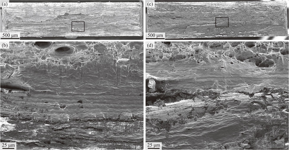
The stress-strain curves obtained from the tensile tests conducted along the RD and TD are reported in Fig. 4. It can be observed that the yield stresses at 0.2% offset were nearly identical along the two directions, with a value of about 370 MPa. However, the tensile stress was higher in the TD with a value of about 440 MPa, indicating a slightly higher work hardening behavior. Both directions showed limited ductility, with a maximum elongation to failure of about 2% for the RD specimen. The fracture surfaces of the tensile specimens were observed by SEM and are shown in Fig. 5. It was found that both specimens exhibited the presence of flat, cleavage-like surfaces, which are typical of brittle fracture. However, there were also areas with ductile void formation, indicated by the presence of dimples on the fracture surfaces. This suggests that the failure mechanism for these specimens was a combination of brittle and ductile fracture, in agreement with reported literature.22)

To better understand the effect of in-plane anisotropy on the tensile behavior of the material, crystal plasticity parameters were determined through inverse analysis by matching the experimentally measured stress-strain curves with those predicted by numerical simulations. The microstructures shown in Fig. 3 were subjected to uniaxial tensile strain with the boundary conditions as depicted in Fig. 3(a). To ensure a uniform out-of-plane displacement, multi-point constraints (MPCs) were applied to nodes on the front face (z = 0.5 µm) while the back face (z = 0 µm) was blocked in the out-of-plane direction. Elastic constants for the two phases were obtained from literature sources.12) In the case of the Nb phase, it was assumed that the strength and hardening behavior of the two slip system families were identical. The crystal plasticity parameters estimated through inverse analysis are summarized in Table 2, and the resulting numerical stress-strain curves are presented in Fig. 4. The agreement between the predicted and experimental curves is acceptable, and the strength anisotropy between the two directions was successfully reproduced. The estimated CRSSs for the two phases indicate that the strength of the Nb phase is higher than that of the Cu phase, which is consistent with previous reports.10,13,14)

Table 2 Crystal plasticity parameters.
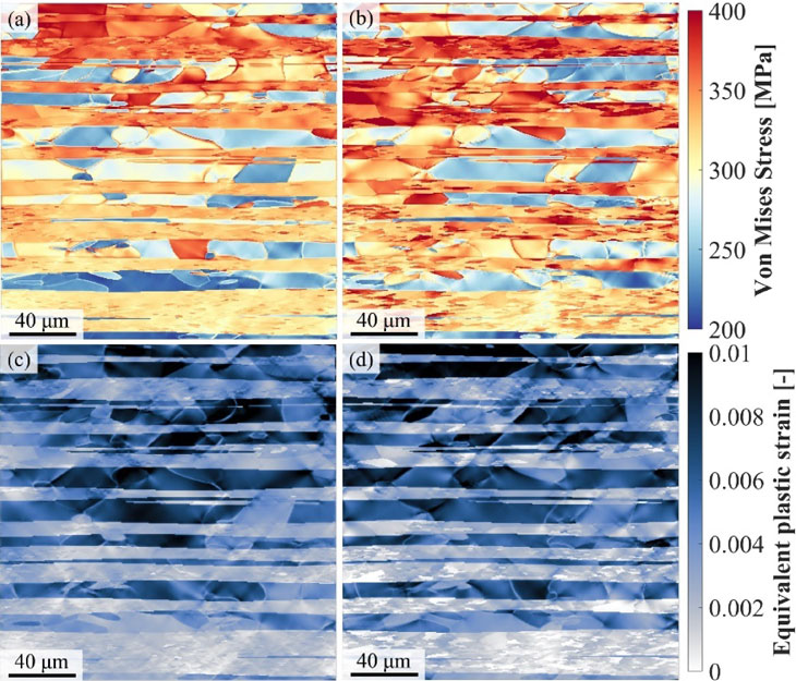
Figure 6(a)–(d) illustrates the von Mises stress field at the 2% applied strain for of the microstructures shown in Fig. 3 under uniaxial tensile strain along either the RD or TD. The stress distribution between the two phases and the two loading directions exhibits significant heterogeneity, with the von Mises stress being higher in the Nb phase, particularly in the vicinity of some interfaces. This large stress gradient is likely the underlying cause of the cleavage-like facets observed on the fracture surface. It is noteworthy that the von Mises stress is greater in the Nb phase when loaded along the TD (Fig. 6(c)–(d)), which can be attributed to the presence of an α-fiber texture (⟨110⟩||RD). Indeed, Nb grains oriented close to this texture tend to exhibit a lower maximum Schmid factor in average when deformed along the TD than along the RD. This may also explain the slightly higher tensile strength in this direction. The low ductility of the material, compared with Nizolek et al.,10) may be attributed to its initial states where Cu grains exhibit significant orientation spread suggesting they are already highly deformed.

The equivalent plastic strain field, shown in Fig. 6(e)–(h), further reveals strain partitioning between the two phases and within each phase between grains. Overall, the plastic activity is predicted to be higher in the Cu phase due to the lower slip strength, with peak intensity of approximately 6% at 2% applied strain. However, some regions of the Nb phase also exhibit some degree of plastic deformation, which often corresponds to the domain between two highly deforming Cu grains on either side of a Nb layer. The discrepancy in strength between the two phases results in early strain localization in some Cu grains, particularly near Cu/Nb interfaces, leading to the emergence of shear bands that propagate across multiple layers and are oriented approximately 45° from the loading direction. This observation is similar to that of Koga et al.32) in the case of a multilayered ferrite/martensite steel sheet who observed similar plastic activity within the soft ferrite and hard martensite. However, not all the highly deformed regions in the Cu phase necessarily propagated through the adjacent Nb layer to form large shear bands, indicating a potential orientation relationship dependence between the two phases for shear banding. This is consistent with previous findings by Jia et al.,14,15) who demonstrated that the development of shear bands is highly dependent on the initial orientation of the two crystals at a given interface. In particular, the presence of the Brass orientation observed in the Cu phase may easily activate shear banding.
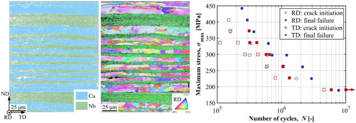
3.3 Fatigue behavior
Figure 7 shows the maximum stresses plotted against the number of cycles to failure for the four-point bending high-cycle fatigue experiments. The arrow indicates a runout specimen. Notably, fatigue life in the RD was found to be higher than in the TD. In-situ observation by OM enabled the determination of the number of cycles for crack initiation, which was predominantly found to occur below the two loading pins on the outer tensile surface due to the positive stress ratio (R = 0.1). It is worth mentioning that for all samples exhibiting a fatigue crack, cracks were observed to initiate in the (Cu phase) outer surface layer. Crack initiation life represented between 35 to 75% of the total fatigue life. Interestingly, cracks tended to nucleate later for specimens loaded in the RD than in the TD for the same maximum stress, indicating the possible influence of the crystallographic texture.

To investigate the effect of texture on crack initiation, CPFE simulations were conducted on multiple synthetic microstructures subjected to four-point bending fatigue conditions. The simulation employed a sub-modeling approach, as illustrated in Fig. 8 and following previous works.28,31) First, a three-dimensional macroscopic simulation representing half of the four-point bending condition was performed. The material behavior was assumed to be isotropic elasto-plastic, with the properties extracted directly from the tensile test results presented in Fig. 4. The specimen was then subjected to ten loading cycles. Next, the nodal displacements obtained from the macroscopic simulation were directly applied as boundary conditions to the edges of the synthetic microstructure (as shown in Fig. 8(c)). The front and back faces are subjected to an imposed z-displacement extracted from the macroscopic simulation. To ensure accuracy, the mesh of the macroscopic model was refined in the region of the imposed displacements (see Fig. 8(b)).

Figure 9 displays an example of von Mises stress at peak load and equivalent plastic strain field accumulated after 10 loading cycles with a maximum stress of 300 MPa. The comparison of these fields with the uniaxial condition presented in Fig. 6 reveals significant differences in terms of their spatial distribution and intensity. The bending condition leads to a higher intensity of both Mises stress and accumulated strain near the tensile surface, which decreases as we move deeper into the material. In contrast, the tensile simulations result in a more homogeneous distribution of both fields. Moreover, the plastic strain field under bending conditions is more heterogeneous, with a significant absence of shear bands propagating across different layers. Instead, the strain is mostly confined within the Cu layers. The Nb layers, on the other hand, exhibit lower plastic activity, but the Mises stresses at peak load are higher. The comparison of the plastic activity between RD and TD shows slightly higher accumulated strain at the outer surface in the TD case suggesting a directional dependence of the accumulated plastic strain.
To better understand the potential cause of the discrepancy in fatigue crack initiation cyclic number, a critical plane fatigue indicator parameter (FIP) based on the combination of the Fatemi-Socie33) and Tanaka-Mura34) criteria was investigated. The FIP is defined by:35,36)
| \begin{equation}
\mathrm{FIP}^{\alpha} = d^{\alpha}\left[\frac{\Delta \gamma^{\alpha}}{2}\left(1 + k\frac{\sigma_{nn}^{\alpha}}{\sigma_{y}} \right)\right]^{2},
\end{equation}
| (4) |
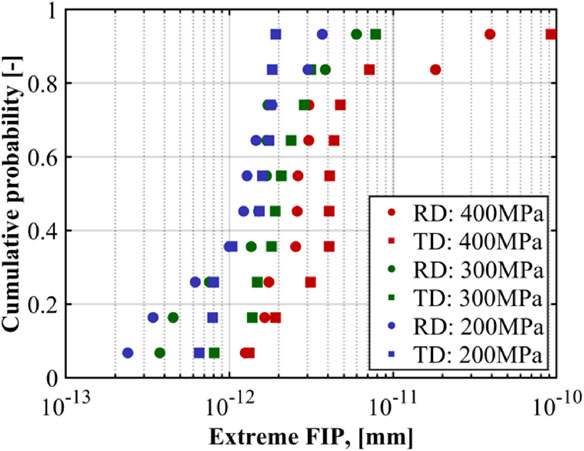
where Δγα and $\sigma_{nn}^{\alpha }$ are the shear strain accumulated in one cycle and the maximum normal stress on the slip system α, respectively. k is a parameter taken to 0.5 and σy is the yield stress. The number of cycles for crack initiation is generally assumed to be proportional to the inverse of the FIP.30) The FIP was analyzed for each individual Cu grain on the tensile surface, along multiple potential crack paths (PCPs) of lengths dα that were defined as the intersection between the slip plane of the slip system α, the normal surface, and the grain boundaries. As such, Δγα and $\sigma_{nn}^{\alpha }$ correspond to the average shear strain and normal stress along the PCP. The detailed procedure for this investigation is outlined in previous research.28,29) This approach allows for a more comprehensive analysis of the potential factors contributing to fatigue crack initiation, as it explicitly considers both the specific morphology of each individual grain and the local heterogeneities of the stress and strain fields. To gather sufficient statistical evidence, ten microstructures were generated following the procedure previously described and exposed to bending fatigue conditions at three maximum stresses: 200, 300, and 400 MPa. Figure 10 illustrates the maximum stress plotted against the extreme FIP for the most critical site for crack initiation, which corresponds to the highest FIP per model. As expected, the FIP decreases with the decrease in applied stress due to the decrease in plastic activity and peak stress. Notably, on average, the RD microstructures exhibit a lower FIP than the TD microstructures, indicating that the crack initiation life is generally longer for the RD specimens. This finding is consistent with the experimentally estimated crack initiation lives presented in Fig. 7 and suggests that the crystallographic texture of the material plays an important role in determining the fatigue behavior of the material. This can be explained by the fact that when loaded along the RD direction, the grains of the material tend to deform slightly more uniformly (Fig. 9(c)), reducing the strain concentration.
Once a crack initiated on the outer tensile surface, it propagated first on the outer surface, perpendicular to the tensile stress direction and then in the thickness direction across the different layers. For the same applied stress, the crack propagation stage also appeared longer for RD specimens than for TD specimens suggesting that crack growth rate was slower in former ones. This is particularly noticeable at 300 MPa in Fig. 7. These trends are attributed
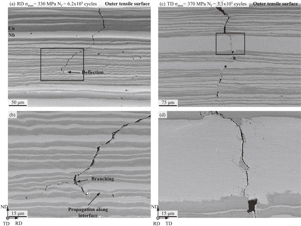
to anisotropy due to texture, contrary to the findings of Radchenko et al.,20) who showed that the interface shear strength may have an influence on the crack growth mechanism in ARB Cu/Nb nanolaminate when the deformation is along RD or TD due to the specific orientation relationship at the interfaces. In the present study, this effect is not observed as the individual layer thickness is of micrometer size and no orientation relationship has developed at interfaces yet, which is consistent with previous studies.2,5) Figure 11 depicts typical examples of crack paths in the thickness direction for RD and TD specimens observed by SEM. Crack paths appear serrated with multiple deflection visible within thick layers or at layer interfaces. In addition, crack branching was observed, predominantly in RD specimens, where a crack would split into different paths and often propagate along Cu/Nb interfaces (Fig. 10(b)). Such bifurcation may reduce the crack growth rate along the thickness direction and therefore improve the fatigue life along the RD. However, the crack growth was not recorded in the present work and is the subject of future study.
The present results may be compared to previous studies of fatigue in metallic foils. Read37) investigated the tension-tension fatigue behavior (R = 0.1) of copper foils produced by electron-beam-evaporation. The foils were polycrystalline with an average grain size of about 1 µm, with only a few grains through the thickness. However, the fatigue life at the same applied stress was significantly shorter compared to the present study, suggesting that not only the grain size but also the presence of interfaces due to the layered structure, the hardness and texture differences between the Cu and Nb layers may also play a major role in improving the fatigue life. Besides, the presence of residual stresses at the surface of the material, resulting from the rolling process, may also affect its fatigue behavior.38)