Abstract
This review article comprises three contents: 1) a general introduction of liquid crystals (LCs) and their chronological developments until their current status, 2) the descriptions of the achievements of defect-free and optically high-quality LC displays (LCDs), and 3) the description of the new and alternative methods for improving existing LCD technologies in terms of high-speed response, viewing angles, and power consumption through nanoparticle doping and optical compensation on a laboratory level. When these technologies are successfully developed, they will be used in the industry, where the fabrication process will be performed in a large-clean room using automated robotics.
1. Introduction
Currently, liquid crystal displays (LCDs) are used as information displays for televisions, notebook computers, personal computers, desktop computers, mobile phones, car navigators, and a variety of other instruments. They are indispensable in our daily lives and jobs. In this paper we first provide an overview of the history of the evolution of LCD technology from its inception to the present. However, the current state of LCDs has been realized by many accumulations of new technologies over the last 60 years. Thus, an LCD is an example of successful innovation in these centuries. Then, we discuss and introduce how high-performance LCDs were realized in terms of their performances such as optically high-quality and large-area LCDs in the early stages in the 1970s and 1980s and accomplishments in high-speed response, wide viewing angles, and low power consumption by comparing existing technologies with new approaches of doping nanoparticles (NPs) into LCDs and novel asymmetric optical compensation through computer simulations. If these new technologies are successfully realized in the laboratory, they can be applied to large-scale production in a large-clean room with robotics.
2. A brief review of the 60-year history of LCDs
In 1888, the first liquid crystal (LC) was discovered by F. Reinitzer.1) He discovered two melting points at 114.5 °C and 178.5 °C accompanied by the production of beautiful colors. Nowadays, this coloration is used for thermography with cholesteric LCs.
Since then, chemistry and physics research has been primarily conducted by scientists in Europe2)–5) and subsequently in the U.S.A.6) LCs have been categorized into nematic, smectic, and discotic types. They have been understood as rod-like or discotic-type organic molecules of finite order in a temperature range.2)–7)
LCD research started with thermography8) and infrared-phonics9),10) using cholesteric LCs. The electro-optic effect in nematic LCs abbreviated as PAA (p-azoxyanisole) was discovered by R. Williams at RCA Corp. in 1962.11) After that, G.H. Heilmeier and his colleagues at RCA developed the first LCDs called dynamic scattering mode (DSM) LCD12) and guest-host LCD.13) In 1968, RCA demonstrated the world’s first digital clock using a DSM LCD, as shown in Fig. 1.14),15) This piqued keen interest in LCs and LCDs globally. In 1970, S. Kobayashi et al. published a book on LCs and LCDs in which they predicted the possibility of digital calculators using LCDs due to the low power consumption of LCDs compared with existing calculators using light-emitting tube displays.16)

In 1973, SHARP Corp., Japan developed and sold the world’s first digital calculator using DSM LCDs, where DIC corporation (the former company name was Dainippon Ink and Chemicals, Incorporated) provided useful LC materials and necessary ionic molecules (Fig. 2).17),18)
Figure 3 shows the historical development of LCDs and organic light-emitting diode (OLED) displays. Currently, 4K and 8K LCD TVs are available, and OLED displays are used in smartphones and partially in TVs.
The chronological developments of appliances using LCDs and OLEDs are as follows:
-
1973: Digital calculators using DSM LCDs
-
1984: Portable LCD TVs
-
1988: 14′′ LCD TV
-
1991: Notebook PCs
-
1992: Digital videos
-
1995: Digital cameras
-
1997: PC monitors
-
2001: LCD TVs
-
2005: 65′′ LCD TV
-
2007: Smartphones
-
2015: 8K LCD TV
-
2018: OLED smartphones
-
2018: OLED TVs
-
Supplement: 2007 Metaverse, VR.
In the following, we shall describe the 60-year history of the development of LCDs.17),19)
In 1971, M. Schadt and W. Helfrich,20) and J. Fergason21) independently invented twisted nematic (TN) LCDs. TN LCDs have become one of the standard LCDs for digital watches and calculators and later for PC monitors since the 1980s. Then, in 1984, T. Scheffer and J. Nehring invented 540 × 270 dot-matrix super TN (STN) LCDs.22)
Therefore, it was necessary to fabricate defect-free LCDs with high optical quality for practical applications. To realize defect-free LCDs, S. Kobayashi and his colleagues successfully fabricated defect-free LCDs,23)–25) which will be discussed and introduced later in Section 3, and E.P. Raynes successfully removed reverse twist disclinations in LCs by doping them with chiral molecules to fabricate a cholesteric LC.26)
The development of the operation principles of LCDs is evidenced by the development of vertically aligned (VA) nematic LCDs,27),28) ferroelectric LCD (FLCD),29),30) in-plane switching (IPS) LCDs,31) and fringe field switching (FFS) LCD.32) These LCDs are currently and widely used in producing televisions, computers, mobile phones, and various instruments, including Metaverse and virtual reality (VR).
The monographs17),19),33),34) describe LCD technologies in detail. Above all, the books written by D.-K. Yang and S.-T. Wu33) and by D.J.R. Cristaldi, S. Pennisi, F. Pulvirenti34) thoroughly describe LCDs with full citations of literature. Furthermore, a monograph edited by K. Okano and S. Kobayashi well described the physics of LCs and the fabrication and characterization of LCDs.35) Books by P.G. de Gennes36) and S. Chandrashekar37) are standard textbooks on the physics of LCs.
3. Structures and operation principles of LCDs
In this section, we describe the structures and operation of all existing LCDs.
3.1. Current existing and advanced LCDs.
Figure 4 depicts the current LCD structure, which includes 2-dimensional thin film transistor drivers, resulting in several pixels of up to 4K and 8K (3840 × 2160, 7680 × 4320 RGB pixels, respectively: ITU-BT.2020: Parameter values for ultra-high definition television systems for production and international programme exchange. https://www.itu.int/rec/R-REC-BT.2020) and a large area with 80-inch diagonals. The red, green, and blue cell color filters were invented by T. Uchida in 1981.38)
In 1979, P.G. Le Comber et al. introduced amorphous Si transistors in the U.K.,39) and this technology was mainly developed by Japanese companies.17),19),40) This enabled the extensive use of LCDs in our society as computers, televisions, and mobile phones,17),19) where all the kinds of LCDs are illuminated by light-emitting diode backlight.
Based on these facts, LCD technology is an excellent example of a successful innovation made in the 20th and 21st centuries.
3.2. TN LCDs.
Figure 5 shows the structure and operation principles of TN LCDs. Under the quiescent condition (Voff), the LC conformation has a 90° twist by adding a chiral agent. With the crossed polarizers, the electric field of incident light rotates along the twisted LC molecules and transmits, resulting in the white state (called normally white). When an operating voltage (Von) is applied, the LC molecules take a vertical conformation except for the two boundary regions, where strong anchoring of the LC molecules is achieved. The transformation of the LC molecules from the planar conformation to the vertical conformation is caused by the torque equation:
| \begin{equation}
\gamma_{1}\frac{\partial \phi}{\partial t} = K_{2}\frac{\partial^{2}\phi}{\partial t} + \varepsilon_{0}\Delta \varepsilon E^{2}\sin\phi \cos\phi,
\end{equation}
| [1] |
where Δε
E2 denotes the dielectric torque force with the positive dielectric anisotropy Δε.
Figure 6 explains normally white and black operations in voltage–transmission (V-T) curves. The existing threshold voltages are also shown in the V-T curves, where the transmission abruptly changes.
Nowadays, TN LCDs are widely used in desktop PCs, notebook PCs, and indicators for all kinds of measuring instruments such as thermometers. An STN LCD is a TN LCD variation, where the twisting angle is increased up to 170°–270° rather than 90°. An STN LCD has a high direct multi-plex that enables it to exhibit 540 × 270 dot-matrix displays due to a sharp V-T curve.22) Conversely, in a TN LCD without using a thin film transistor driver, multiplexing is limited to the seven-segment display.
3.3. Electrically controlled birefringence (ECB) LCDs.
Figure 7 depicts a cross-sectional view of an ECB LCD and its operation principle.35) This device is also designated as a tunable birefringence LCD. Under the quiescent condition (Fig. 7a), LC molecules with a pretilt angle are oriented to be 45° to the transmission axes of the crossed polarizer; this situation produces the white state by illuminating this device from the bottom direction. The generation of the pretilt angle ensures defect-free LCDs. Under an operation voltage (Fig. 7b), LC molecules take a slated conformation in unison due to the positive dielectric torque. In the Appendix, we explain the optical effect in an optical system, where a planar LC cell with optical anisotropy is sandwiched between the crossed polarizers. This effect occurs commonly in all types of LCDs.
3.4. IPS and FFS LCDs.
Figure 8 shows the structure and operation principles of IPS and FFS LCDs with the driving electrodes (designated as inter-digital electrodes), rubbing direction, and LC molecular switching.31),32)
In the two LCD devices, LC molecules are aligned and switched in a plane. Under the quiescent condition, LC molecules are oriented at an angle to yield the white state; LC molecules with a positive Δε rotate in the plane when an operation voltage is applied to the electrodes. When the direction of LC molecules takes 45° to the edge direction of the crossed polarizers, the LC device produces the white state. When the angle is null, the device produces the black state.
An IPS LCD with a negative Δε is also available. IPS LCDs have a wide angle of view; thus, they are widely used in LCD TVs, advanced notebook PCs, and VR.
3.5. VA LCDs.
Figure 9 shows the structure of VA LCDs and their operation principles. Under the quiescent condition (Voff), a VA LCD produces a black state with the crossed polarizers. When an operation voltage (Von) is applied, LC molecules with a negative Δε take an inclined conformation, resulting in the white state,27),28) where the rubbing direction is set to be 45° to the axes of the polarizers to generate a pretilt angle for producing defect-free VA LCDs. A VA LCD has a high contrast ratio and is widely used in LCD TVs.
3.6. Optically compensated bent LCDs.
Figure 10 shows the structure of optically compensated bent (OCB) LCDs with a biaxial optical compensator. In an OCB LCD, LC molecules are aligned in a bent conformation; this device is designed for normally white operations by applying a bias voltage of 1.6 V. When an operation voltage is applied, this device exhibits a black state by switching the retardation form π to zero. This device has a ten-fold faster response speed compared with other LCDs using nematic LCs.41)
3.7. Polymer-stabilized V-shaped switching FLC LCDs.
Figure 11 depicts the molecular switching in a polymer-stabilized V-shaped (PSV) FLC LCD and its V-T curve characteristics.42),43) In Fig. 11A, (a) is the state of the polymer-stabilized ferroelectric liquid crystal display (PS-FLCD) molecules at the quiescent condition (Vappl = 0), where the polymer molecules are red-colored. In (b) the minus electric voltage is applied; then the FLC molecules tend to incline toward the left direction due to their permanent polarization, and in (c) the situation of the positive electric voltage is applied. In these processes, each of the FLC molecule slide and rotate on a cone like structure. In this figure, all the FLC molecules are represented as a projected figure on a plain. Under the crossed polarizers, the configurations (b) and (c) produces white state, whereas in (a) the black state is produced. In Fig. 11B, we show the electro-optical performance of the polymer stabilized V-shaped switching FLCD, called PSV FLCD that exhibits V-shaped gray scale operation. While, the ordinary FLCD exhibits a hysteresis operation with a memory capability.

The conventional FLC LCD exhibits hysteresis characteristics and bi-stability in its V-T curve. In contrast, a PSV FLC LCD exhibits a continuous grayscale IPS. This was demonstrated for the first time.
3.8. Color filter-less field-sequential LCDs.
Figure 12 shows how a full-color image will be constructed in the switching process of a field-sequential (also designated as color-sequential) LCD accompanying the timing chart in this device, where the switching of the backlight is performed sequentially in the order of R–G–B, each with a switching-on-time of 4.6 ms and the related switching on and off the LCD. Thus, it is required that τ = τon + τoff < 4.63 ms.43),44)
An FSC LCD has 30% low power consumption and exhibits three-fold higher lightness than color filter-based LCDs. Field-sequential full-color LCDs have been fabricated by using PSV FLCDs and narrow gap TN LCDs, with the latter being used as airport indicators in the baggage claim area.
4. Conditions for designing take-off in LCDs in the early 1970s and 1980s
Room-temperature LC materials are required to create practical LCDs; initial examples are shown in Table 1.45),46) Nowadays, practical LC materials are well developed.47),48)

Table 1. Initial room-temperature LCs
Among them, 5CB (4-cyano-4′-pentylbiphenyl)44) exhibits positive dielectric anisotropy and plays a role in fabricating TN LCDs. However, nowadays, LCs used in displays are eutectic mixtures of multiple components47),48) that can withstand a wide temperature range from −20 °C to 100 °C. In addition, such LCs should exhibit high resistivity, positive and negative large dielectric anisotropy, and low viscosity.
Now, we will summarize the dominant factors constituting the take-off in LCD technology as follows17),19):
-
1)
inventions of operation principles of various LCDs,
-
2)
syntheses of room-temperature LC materials that will be driven by an electric voltage of approximately 5 V,
-
3)
realization of defect-free, optically high-quality, and large-area LCDs using a rubbing machine and photo alignment,
-
4)
full-color LCD using in-cell color filters,
-
5)
improvement of viewing angle,
-
6)
improvement of the response speed of LCDs and power consumption, and
-
7)
the adoption of thin film transistor drivers for realizing LCDs with high information contents.
In the succeeding sections, we will focus on items 3), 4), and 5) and conduct experiments with them on a laboratory scale. Some of them are mass-produced.
5. Realization of defect-free, optically high-quality and large-area LCDs
5.1. Elimination of disclination defects and the demonstration of multicolor TN LCDs.
As mentioned in Section 2, the invention of TN LCDs20),21) in 1971 opened a new era of LCD technology for the fabrication of digital watches and calculators. However, optical defects degrade the optical quality of TN LCDs; these are reverse twist disclinations and reverse tilt disclinations as shown in Figs. 13 and 14, respectively.23),24)
In 1972, F. Takeuchi, a staff of BUSICOM Corporation in Osaka, became a visiting researcher at RIKEN, Saitama, Japan, where S. Kobayashi conducted LC research as a member of staff at RIKEN. In the early stage of the research, Takeuchi observed the appearance of unfamiliar patterns in TN LCD cells. He inquired “what are they?” Kobayashi explained that they are “disclinations (disinclinations) originating from the discontinuity of refractive indices and are visible when the TN cell is sandwiched between two closed polarizers”.49)
The structure and operation are shown in Fig. 5. However, it is impossible to fabricate optical defect-free TN LCDs. To fabricate defect-free TN LCDs, it is necessary to provide a pretilt angle, which is provided in advance before applying the operation voltage by performing the rubbing process on both substrates. Thus, the entire inclination of the LC molecule system is performed in unison, as will be introduced and discussed in the following parts of this paper. An illustrative explanation of the pretilt angle generation is presented in the Appendix.
When the splay and bent conformation coexist in a 90° twisted cell, the reverse twist disclination occurs, which causes light leakage and degrades optical contrast in the black state in the TN LCD cell. Takeuchi proposed an off 90° twist, i.e., 88° twist conformation that has lower energy than that of a 90° twist. This method was very effective and was granted a U.S. patent.25) In 1974, E.P. Raynes invented an alternative to our method; he proposed a method of doping chiral molecules such as a cholesteric LC.26)
Figure 15 shows the molecular conformation of the existing reverse tilt disclination in the TN LCD cell without a pretilt angle in both substrates. If there is no pretilt angle, there is no reverse tilt disclination.35),49) Based on the abovementioned research work, we demonstrated defect-free color TN LCDs, as shown in Fig. 16.23),24),49)
Figure 16 was obtained by Kobayashi and Takeuchi through collaboration with facilities at both RIKEN and BUSICOM Co. The results shown in Fig. 16 were demonstrated at RIKEN in October 1972, and many people saw a working TN LCD for the first time. The same demo was also performed at Tokyo Institute of Technology. It was also presented at the 1973 SID International Symposium23) and published in The Proceedings of SID in 1974.24)
The TN LCD shown in Fig. 16 was fabricated using a prototype of the rubbing machine; its practical version was invented by S. Kobayashi in 1972–1973.22),23),48) The rubbing machine consists of a metal cylinder wrapped with a fabric such as a woolen close, and the cylinder is rotated and horizontally transferred to rub the substrate plate covered with a transparent electrode and polymer film-like polyimide, where the pressure of the cylinder on the substrate is precisely controlled to determine the rubbing strength. Currently, such rubbing machines with the same principle and cylinder structure are in laboratories and factories around the world. The original rubbing machine shown in Fig. 17 is preserved in the Memorial Room at RIKEN as her 100-Year Anniversary.49)
5.2. Realization of defect-free and large-area STN LCDs.
In the 1980s, digital LCD watches and calculators were manufactured using the technique of oblique vacuum evaporation of oxide materials to realize LC molecular alignment with an appropriate pretilt angle.50) The scanning vacuum evaporation technique is available even though this technique is inferior to the rubbing technique during the mass production of large-area LCDs, which will be introduced subsequently.
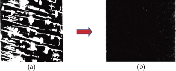
In 1984, an STN LCD was reported,22) fabricated using the scanning vacuum evaporation technique. In this STN LCD, when the pretilt angle is as low as that of TN LCDs, the stripe domain appears, as shown in Fig. 18a, which significantly reduces the contrast ratio.
To remove the stripe domain, H. Fukuro and S. Kobayashi modified the surface of a polyimide polymer by attaching alkyl branches to polyimide alignment molecules, as shown in Fig. 18a, and applying the rubbing process to them. Through this technique, they successfully produced high pretilt angles of 7°–10° (Fig. 18b) and fabricated a defect-free STN LCD.52)–54) This kind of STN LCDs were adopted for fabricating the world's first notebook PC Toshiba DynaBook (Fig. 19) and word processors.17)
In Fig. 20, the pale gray color represents LC molecules, the blue color represents molecules used in achieving a pretilt angle through rubbing, and the red color represents UV reactive molecules doped and migrated to the surface; this technology is called self-surface alignment, which requires no preliminary rubbing or applied voltage during UV photocuring.55),56)
5.3. Realization of defect-free FLC LCDs.
In 1980, an FLC LCD with a fast-switching speed of sub-millisecond was reported.29),30) This LCD piqued keen interest among many people. However, a severe challenge was encountered: a zigzag defect that degrades optical contrast. Nonetheless, this defect was again removed by the Kobayashi group using a very flat polymer alignment film, RN-1199, Nissan Chemical Co. as demonstrated in Fig. 21.42)
This zero pretilt angle method is also useful for fabricating IPS and FFS LCDs.
Using a defect-free PSV FLCD, we fabricated color filter-less field-sequential defect-free FLCD 4-inch SVGA 800 × 600 pixels (Fig. 22).43)
The technology of the color filter-less field-sequential color TN LCD was invented by H. Hasebe and S. Kobayashi in SID 1985.44)
The conventional FLCD demonstrates a bi-stable electro–optical operation; however, the adoption of polymer stabilization brings symmetric and V-shaped electro–optical characteristics.42),43)
Nowadays, photo alignment technology is widely used for manufacturing various LCDs instead of the rubbing process.57)–60)
5.4. Realization of defect-free and multidomain TN LCDs using photo alignment.
Figure 23 depicts a representative photo alignment method, where the polymer film is first irradiated vertically with a polarized UV light, and then, the substrate is rotated by 90° and irradiated with the oblique polarized UV light.60) This technology achieved four domains in a pixel and provide a wide viewing angle.61) This method had a positive impact on 10th generation LCD TVs.61)
5.5. Theoretical considerations and explanations of surface alignment of the treated substrates.
Regarding the physics of LC alignment in LCDs, we used lessons learned from our life mentor, Professor Koji Okano, who taught us statistical mechanics such as the steric interaction between LC molecules and substrates62) and quantum mechanics for anisotropic van der Waals force,63) to achieve uniaxial alignment of LC molecules; stick and slip in tribology will be the generation mechanism of pretilt angles, and the rubbing process that causes optical anisotropy in the treated substrates64) will be the origin of the uniaxial alignment of LC molecules, resulting in defect-free LCDs, as shown in Figs. 14 and 16.23),24),49),50) Other examples are alignment on stretched polymer films65) and Langmuir–Blodget films.66)
Regarding literature on LC molecule alignment, a review paper by S. Ishihara and M. Mizusaki67) and other books68),69) provide a thorough introduction to LC molecule alignment in LCDs.
6. Improvements in the performance of LCDs
6.1. Existing technologies for increasing the viewing angle in LCDs using optical compensation.
The first invention for increasing the viewing angle in TN LCDs was demonstrated by H. Mori at Fujifilm Co. using a discotic LC.70) Then, many related studies have been conducted such as the work by T. Miyashita et al.,71) K. Ono,72) and H.L. Ong.73)
Figure 24 demonstrates how to realize a wide viewing angle in TN and OCB LCDs by optical compensation. Figure 24a shows ISO transmission curves with viewing angle dependence; however, the transmission is homogeneous.71) M. Kitamura performed computer simulations of electro–optical performance of LCDs.74)
6.2. New alternative methods for increasing the viewing angles and optical uniformity in NP-doped LCDs.
The basic idea and motivation for doping NPs of size >100 nm is to modify the properties of LCs governed by the order parameter and optical properties, as discussed in a previous paper.75)
Figure 25 shows an example of the increase and broadening of the optical output intensity in a 0.05-wt.% SiO2 NP-doped ECB LCD.76)
Figure 26 shows argon laser light projected on a screen after passing through TN LCDs, where (a) shows TN LCDs without NP doping, and (b) shows a 0.075-wt.% PγCd-ZrO2-doped TN LCD cell. As shown in Fig. 26a, diffraction and laser speckle patterns are observed, whereas, in Fig. 26b, the optical pattern becomes uniform. The reduction in the number of speckle-patterns and crosses may be attributed to the forward optical scattering by NPs, and thus, de-coherence occurs when light passes through the NP-doped ECB cell, where the size of the NP is significantly smaller than the optical wavelength. This type of optical scattering will be analyzed with Rayleigh–Gans criteria such that
| \begin{equation*}
2ka| m - 1 | \ll 1,
\end{equation*}
|
where
k represents the wave number for light with wavelength λ propagating in a medium with a refractive index ratio
m between
nnanoparticle and
nmedium, and
k = 2π/λ = 2π
nmedium/λ
VAC, and
a represents the radius of the NP. In this system, the diameter of the NP is ∼7 nm, and the wavelength of light is 488 nm, which satisfies Rayleigh–Gans criteria.
76)
6.3. Reduction of the threshold voltage and that of the power consumption in NP-doped LCDs.
Figure 27 demonstrates that doping of MgO NPs reduces the threshold voltage of TN LCD by 26%.77)
The threshold voltage can be written as
| \begin{equation*}
V_{\textit{th}} = \pi \sqrt{\frac{K}{\varepsilon_{0}\Delta \varepsilon}},
\end{equation*}
|
where
K represents the elastic constant, and Δε denotes dielectric anisotropy and is proportional to the order parameter. Then, the relative threshold voltage against that of the order parameter is given as
| \begin{equation*}
\Delta V_{\text{th}}/V_{\text{th}} = (1/2) \Delta S/S.^{78)}
\end{equation*}
|
As shown in
Fig. 27, a 26% reduction in the threshold voltage results in a 50% reduction in the order parameter: This is an extreme case. In most cases, the quantity values of the Vth reduction range from 5% to 10%.
78) This Vth reduction is reproduced by raising the temperature by 10 °C; this temperature is known as the Kobayashi temperature.
75) This suggests that doping NPs into LCs could effectively increase temperature.
74),76) Power consumption in LCDs is proportional to the square of the applied voltage; thus, the reduction in Vth by NP doping reduces the power consumption of LCDs. A good example of the reduction in power consumption is introduced in the following.
We proposed that the power efficiency of a display be characterized by luminance efficiency (LE), defined as
| \begin{equation*}
\mathrm{LE} = \mathrm{cd}/\mathrm{W},
\end{equation*}
|
where cd is the unit for luminance and W is the unit of power consumption for one square meter by assuming that power consumption is proportional to the display area (
Table 2). Herein, we compare the LE of a standard commercial LCD TV and an NP-doped field-sequential TN LCD; their LE values are 1.95 and 5.13, respectively. According to the standard value of The Energy Star Program version 5.3 (
https://www.energystar.gov/products/spec/television_specification_version_5_3_pd), LE is 3.8 (cd/W).
Table 2. Quantitative numerical values of LE (cd/W)
| |
LCD TV (SHARP) 60′′ |
FSC LCD |
| [A] Luminance (cd/m2) |
450 |
1,050 |
| [B] Power (W/m2) |
230/1.00 (=230) |
1.92/0.0094 (=204) |
| [A]/[B] LE (cd/W) |
1.95 |
5.13 |
According to the Energy Star Program (ESP) version 5.3, the power consumption of LCD TV with 50 inches in the diagonal must be 108W or less. The ESP gives luminance efficiency (LE) = 3.8 (cd/W).
The numerical value of our LCD is 2.63 times better than current commercial LCD TVs in terms of power consumption.17),19) Another advantage of NP doping is the significant increase in color gamut in LCDs, but this topic is left in Refs. 17 and 19.
6.4. Quantum dot (QD).
Figure 28 shows the structure of QD, with (a) showing the core/shell, (b) the energy band structure, and (c) the actual structure of core/shell/and ligand and their sizes.79) A QD is a single crystal composed of nano-sized semiconductors as a novel photo-luminescence device for the backlight of LCDs.
Examples of the core/shell are as follows:
-
CdSe/ZnS,ZnSe. Cd-free materials, including InP/ZnS,InP/ZnSe.
-
InP/ZnS,InP/ZnSe. Another Cd-free material is Perovskite: CsPbX3 (X = Cl, Br, and I).
Ligand molecules such as oleic acid were adopted to prevent the segregation of QDs kept in an organic solvent before they are used to construct the LCD backlight. The design of the core/shell structure is to realize a long exciton lifetime. Photo-luminance produced by the illumination using a blue light source is red, green, and blue lights with a narrow half-value width, depending on the size.79)
7. Improvement of response speed in LCDs
The residual technical issue in LCDs that will be resolved is their slow response speed.
7.1. Existing technologies for increasing the response speed of LCDs.
As mentioned above, LCDs are widely used as information displays for televisions, computer monitors, and various instruments. However, their response speed needs further improvement. To this end, several methods have been adopted as follows: (1) using LC materials with low viscosity,47),48) (2) devising electrode structures,80),81) (3) doping with chiral agents,75) (4) doping with NPs,75) (5) using ferroelectric LC materials,29),30) (6) using an LCD with a narrow gap cel,82) (7) OCB LCD,41) (8) blue-phase LCD,83) and (9) overdriving the voltage threshold to increase the response speed during the switching-on process.84)
In the following, we shall describe two novel-alternatives to these existing technologies for improving the response speed.
7.2. Improvement of response speed in ECB LCDs using an asymmetric optical compensation system.
Discovery of the generation of the temporal effect in asymmetric optically compensated (OC) ECB LCDs and their performance is important.
Figure 29 illustrates the optical system of an OC ECB LCD cell, whose e-axis, e1, is rotated by π/4 from the x-axis, and the e-axis of the compensator (+A-plate), e2, is crossed to e1, where R = 2π(ne − no) d/λ is the optical retardation of each axis 1 and 2, where e and o denote the extraordinary and ordinary refractive index axes, respectively.75)

When the retardation in axes 1 and 2 is equal, the system is symmetric. In contrast, when they are different, the system is asymmetric. In 2015, we unintentionally discovered a slow response speed during the switching-off process of an asymmetric OC ECB LCD, where we chose δ2 = π/2 + α (α = 7°), in contrast to when we chose δ2 = π/2 − α (α = 7°). Then, we obtained a two-fold faster response speed during the switching-off process.75) The geometry phase, which is a historically well-known word, is performed by S. Pancharatnam85) and M.V. Berry.86) However, they did not deal with the temporal effect as a system response to the externally applied field.
The switching angle in the ECB LCD will be the polar angle, θ1 from the z-axis. However, the polar angle, θ1, will be replaced by optical retardation, δ1, as will be given as follows:
| \begin{equation}
\delta_{1} = \frac{2\pi dn_{\text{o}}}{\lambda}\left\{\cfrac{1}{\biggl[1 - \biggl(1 - \cfrac{n_{\text{o}}^{2}}{n_{\text{e}}^{2}} \biggr)\sin^{2}\theta_{1} \biggr]^{1/2}} - 1 \right\}.
\end{equation}
| [2] |
shows the relationship between δ
1 and θ
1 by the cell gap,
d = 2.78 µm.
Now, we shall derive a formula for the optical transmission in our optical system by updating previous work.75)
In the ECB LCD, the normalized optical transmission of the single cell reads
| \begin{equation}
T_{1} = \sin^{2}(\delta_{1}/2),
\end{equation}
| [3] |
where δ
1 represents the optical phase delay between the
e-axis and
o-axis for the incident light wave.
Equation [3] produces the normally white state when δ
1/2 = π/4. The normalized optical transmission of the OC ECB LCD is given as
| \begin{equation}
T_{2} = \sin^{2}[(\delta_{1} - \delta_{2})/2].
\end{equation}
| [4] |
When δ
1 = δ
2,
T2 = 0 and the optical system shown in
Fig. 29 becomes symmetric; under this condition, the system produces a black state, as shown in
Fig. 21. If we insert δ
2/2 = π/2 − α into
Eq. [4], we have
| \begin{equation}
T_{2} = \cos^{2}[(\delta_{1}/2 + \alpha)].
\end{equation}
| [5] |
This means that
T2 has a phase advancement α in δ
1/2. This phase advancement generates a temporal effect that produces a two-fold faster response during the switching-off process, as reported in a previous paper.
61) Regarding the switching-on process, there is no optical compensation effect due to the overdriving effect from the driving electric field.
84)
7.3. Generation of temporal effect in asymmetric OC IPS and FFS LCDs.
We shall then proceed to asymmetric OC IPS and FFS LCDs by extending to this field from the asymmetric OC ECB LCD given in Section 7.2.
Figure 31 illustrates the optical system of OC IPS and FFS LCDs, where e1 and e2 denote the e-axes of the active LCD and compensator, respectively.87)
In OC IPS and FFS LCDs, the switching angle is represented by ϕ1, and ϕ2 represents the setting azimuthal angle of a compensator (+A-Plate), whose angle is set to ϕ2 = 3π/4 − α, which can be controlled using a dynamic retarder when we use an IPS cell as the compensator. When α = 0, the system is symmetric with ϕ1 = π/4.
The entire system is sandwiched between crossed polarizers, where the incident light field into the LCD system is polarized in the x-direction and the transmitted wave is polarized in the y-direction. Labels e1 and o1 in Fig. 31 indicate the axes of the extraordinary and ordinary waves, respectively, and labels e2 and o2 indicate those of the compensator, respectively.87)
7.A. Analytical derivation of normalized optical transmission of a single IPS cell.
Using the system shown in Fig. 31, we perform a 2 × 2 Jones matrix calculation33) for the I1 of the single cell.
The input electrical field is
| \begin{equation}
\begin{bmatrix}
1\\
0
\end{bmatrix}
E_{0}.
\end{equation}
| [6] |
After performing Jones matrix calculations, we obtained the normalized optical transmission for the IPS single cell such that
| \begin{equation}
T_{1} = \sin^{2}(2\phi_{1}).
\end{equation}
| [7] |
For the asymmetric OC IPS LCD, we obtained the normalized transmission with a phase advance by α:
| \begin{equation}
T_{2} = \cos^{2}(2[\phi_{1} + \alpha]).
\end{equation}
| [8] |
In Ref. 87, a full description of the Jones matrix calculations for deriving these equations is given. In our system, the symmetry breaking causes a phase shift, which leads to a fast response during the switching-off process. This effect is shown in Table 3. When the LC cell and A-plate are crossed, ϕ1 = ϕ2 = π/4 and δ1 = δ2 ≈ π; then, the symmetric system produces a black (dark) state and no ultrafast switching process occurs.
Table 3. Results of response time for the n-OC IPS device
| |
Single n-IPS |
n-OC IPS
(α = 0) |
n-OC IPS
(α = −6.8°) |
| τoff (msec) |
25.6 |
25.1 |
14.9(42% decrease) |
| Vop (V) |
6.8 |
9.1 |
15.0 |
8. Experimental measurements
8.1. Optical configurations and switching of single and OC IPS and FFS LCD cells with Δε > 0 and Δε < 0.
Figures 32 shows the optical configurations and switching of single and OC IPS and FFS LCD cells used in this study, where p and n denote Δε > 0 and Δε < 0, respectively.
Next, we explain the switching process in our OC LCDs, along with the contents of Fig. 33. This figure shows simulation results for the normalized transmission and compares T1 (I1) with T2 (I2) against the switching angles calculated using Eqs. [7] and [8].
The top and central parts in this figure show the behaviors during the switching-off process, and the bottom and right parts show the behaviors during the switching-on process. Thus, ϕ1 for T2 (I2) starts from −α°, and ϕ1 for T1 (I1) starts from 45°.
The results in Fig. 33 are interpreted as follows:
(1) T2 (I2) has a phase advancement of α over T1 (I1);
(2) According to the top area, T2 (I2) starts the decay process with a finite inclination, whereas T1 (I1) starts the decay process with no inclination. This decay in the absence of inclination is attributed to the fast response in the decay process, which has been experimentally demonstrated in this study. This phenomenon is a purely optical effect, with the decay process occurring as the common molecular relaxation for both symmetric and asymmetric systems.
(3) T2 (I2) has a finite value at the right bottom because of energy conservation, which means that the operation is not normally black. The realization of a normally black operation is described in Section 3.4.
8.2. V-T curves of single p-IPS and p-OC IPS LCDs.
Figure 34 shows the experimentally obtained V-T curves of IPS LCDs, as recorded at 25 °C using a DMS-703 (Autronic Melchers, GmbH) instrument. Interestingly, in the symmetric compensation system, the introduction of optical compensation produces a wide operating voltage range, as shown in Fig. 35. The V-T curve with the Freedericksz transition is described in a book.33)
Figure 35 shows the V-T curves of the p-OC IPS devices without optical compensation (α = 0) and with optical compensation (α = −6.8°). The proposed asymmetric OC IPS produces T = 0 at 4 V, indicating a non-normally black operation. In general, an LCD is operated as normally black or white; thus, the normally black operation was achieved using a dynamic optical compensator (retarder), which was fabricated in our work.87) A simulation was also performed on this problem, as given in Section 10.
8.3. Experimental results of response time.
The physical properties of the LC materials and the specifications of the LCD cells used in this study are described as follows: The cell gap of the sample cells was 3.5 µm, and the wavelength of the optical light source was 589 nm. The anisotropy of refractive indexes and dielectric constants of used nematic liquid crystal materials are given in Table 4.
Table 4. Numerical values of the anisotropy of refractive indexes and anisotropy of dielectric constants of the used nematic liquid crystals*
| |
Δn (589 nm, 25 °C) |
Δε (25 °C) |
| p-IPS |
0.088 |
6.2 |
| n-IPS |
0.110 |
−4.1 |
| p-FFS |
0.110 |
11.9 |
| n-FFS |
0.110 |
−4.1 |
*) After Datasheet of DIC.
Based on these quantities, the experimental results in Tables 3 and 5 indicate that the response time of the proposed asymmetric OC IPS device was reduced by 42%–56% compared with that of single cell OC IPS devices. The same results were obtained for the ASOC FFS device, and we will report the corresponding data elsewhere. The results for the switching-on process indicate that the response time will be significantly reduced by adopting the overdriving technique.86)
Table 5. Results of response time for the p-OC IPS device
| |
Single p-IPS |
p-OC IPS
(α = 0) |
p-OC IPS
(α = −6.8°) |
| τoff (msec) |
18.3 |
14.1 |
8.1(56% decrease) |
| Vop (V) |
4.0 |
4.5 |
5.5 |
9. Temporal derivatives of I1 and I2 and their comparison
Here, we derive temporal derivatives of I1 and I2 as
| \begin{equation}
\frac{\partial I_{1}}{\partial t} = \frac{\partial I_{1}}{\partial \phi_{1}}\frac{\partial \phi_{1}}{\partial t} = 2I_{0}\sin(4\phi_{1})\frac{\partial \phi_{1}}{\partial t}.
\end{equation}
| [9] |
For an OC IPS:
| \begin{equation}
\frac{\partial I_{2}}{\partial t} = \frac{\partial I_{2}}{\partial \phi_{1}}\frac{\partial \phi_{1}}{\partial t} = - 2I_{0}\sin(4\phi_{2} - 4\phi_{1})\frac{\partial \phi_{1}}{\partial t},
\end{equation}
| [10] |
| \begin{align}
&= - 2I_{0}\sin(4\phi_{1})[\cos(4\alpha) \\
&\quad- \sin(4\alpha)\cot(4\phi_{1})]\frac{\partial \phi_{1}}{\partial t}.
\end{align}
| [11] |
Thus, we obtain a formula, the F-function, by taking the ratio between Eqs. [9] and [11] as follows, where the two minus signs cancel each other:
| \begin{equation}
F = \cos(4\alpha) - \sin(4\alpha)\cot(4\phi_{1}).
\end{equation}
| [12] |
The F-function $( \frac{\partial I_{2}}{\partial t}/\frac{\partial I_{1}}{\partial t} )$ is shown in Fig. 36. This figure shows that the temporal derivative of I2 is significantly larger than that of I1 during the switching-off process, which is consistent with the experimental results obtained in this study. However, it also shows that this effect terminates at a switching angle of 15° and that the relation is thereafter inverted. However, if necessary, a dynamic compensator can be used to stop the phase advancement after the decay process for the switching-on process, and the removal of the applied voltage causes an overvoltage, resolving this problem.
10. Dynamic compensator
A dynamic compensator changes the azimuthal angle of the e-axis, ϕ2 = 3π/4 − α, by applying a computer-controlled electric voltage, Vappl, according to the following equation:
| \begin{equation}
\alpha = \alpha_{0}\exp[1 - kV_{\text{th}}/V_{\text{appl}}],\ k > 1\ (k = 2.5).
\end{equation}
| [13] |
-
(1)
For the switching-on operation (starting from Vappl ≈ 0), the normally black operation will be induced with α = 0 (ϕ2 = 3π/4).
-
(2)
For the switching-off operation, where Vappl = kVth (k = 2.5) and α = α0(∼7°), extra phase, α, is generated.
The experimental results are reproduced through computer simulations using a computer simulator: SHINTECH-LCD Master (Fig. 37).
11. Conclusions and summary
-
1.
A brief history of the chronological development of LCDs is presented, including a series of the inventions of LCD modes.
-
2.
Advancements in key and existing technologies that led to the achievement of the current LCDs are presented.
-
3.
Through the invention of rubbing machines, surface modification, and novel photo alignment technology, we realized a variety of defect-free, optically high-quality, and large-area LCDs.
-
4.
Description of newly developed technologies, alternatives to existing technologies, by doping NPs into LCDs and asymmetric optical compensation for achieving fast response speed and a wide viewing angle are shown.
-
5.
Detailed descriptions of the asymmetric OC IPS, FFS, and ECB LCDs are provided.
-
6.
By the development and adoption of a dynamic compensator driven by applying voltage to this device, we successfully realized the normally black mode operation of the asymmetric OC LCDs. This was reproduced by optical simulations.
Acknowledgments
This research was conducted as a part of The Project MEXT, Yamaguchi Green Materials Cluster. The authors wish to thank Haruyoshi Takatsu and Hiroshi Hasebe at DIC Corp. for their kind and enthusiastic collaboration in LC material research and Kiyofumi Takeuchi at DIC Corp. for his enthusiastic collaboration. The authors are indebted to Shoichi Ishihara at Osaka Institute of Technology for executing the preparation of this paper. Furthermore, the authors thank Professors Kazuo Kuroda, Deng-Ke Yang, and Shin-Tson Wu for providing us with useful instructions to perform the Jones matrix calculation. The authors are deeply indebted to Professor Koji Okano for providing us with helpful instructions on the physics of surface LC alignment and to Professor Tatsuo Uchida for providing us with valuable data.
Notes
Edited by Akihisa INOUE, M.J.A.
Correspondence should be addressed to: S. Kobayashi, Sanyo-Onoda City University, Daigakudori 1-1-1, Sanyo-Onoda, Yamaguchi 756-0884, Japan (e-mail: lcd.kobayashi@gmail.com).
References
- 1) Reinitzer, F. (1888) Beiträge zur Kenntniss des Cholesterins. Monatsh. Chem. 9, 421–441.
- 2) Kelker, H. (1988) Survey of the early history of liquid crystals. Mol. Cryst. Liq. Cryst. 165, 1–43.
- 3) Demus, D. (1988) 100 years liquid crystal chemistry. Mol. Cryst. Liq. Cryst. 165, 45–84.
- 4) Sluckin, T.J., Dunmur, D.A. and Stegemeyer, H. (2004) Crystals That Flow. Taylor & Francis, London, New York.
- 5) Dunmur, D. and Sluckin, T. (2011) Soap, Science, and Flat-Screen TVs: A History of Liquid Crystals. Oxford University Press, Oxford.
- 6) Brown, B.H. and Shaw, W. (1957) The mesomorphic state: liquid crystal. Chem. Rev. 57, 1049–1057.
- 7) Chandrasekhar, S., Sadashiva, B.K. and Suresh, K.A. (1977) Liquid crystals of disc-like molecules. Pramana 9, 471–480.
- 8) Fergason, J. (1968) Infrared thermography using cholesteric liquid crystals. Appl. Opt. 7, 1729–1732.
- 9) Sakusabe, T. and Kobayashi, S. (1971) Infrared thermography with liquid crystals. Jpn. J. Appl. Phys. 10, 756–761.
- 10) Kobayashi, S. (1972) Infrared phonics. Image Tech. Eng. (Gazou Gijutsu) 4, 1–6 (in Japanese).
- 11) Williams, R. (1962) Domains in liquid crystals. J. Chem. Phys. 39, 384–388.
- 12) Heilmeier, G.H., Zanoni, L.A. and Barton, L.A. (1968) Dynamic scattering: a new electrooptic effect in certain classes of nematic liquid crystals. Proc. IEEE 56, 1162–1171.
- 13) Heilmeier, G.H. and Zanoni, L.A. (1969) Guest-host interaction in nematic liquid crystals, a new electro-optical effect. Appl. Phys. Lett. 13, 91–93.
- 14) Castellano, J.A. (2005) Liquid Gold: The Story of Liquid Crystal Display and Creation of an Industry. World Scientific, Singapore.
- 15) Weber, L. (2018) David Sarnoff, display industries vision. Inf. Disp. 34, 12–17.
- 16) Kobayashi, S., Ueno, S., Hirose, T. and Sakusabe, T. (1970) Liquid crystals—their properties and applications. Nikkan-Kogyo Shimbun, 30 September, 1970 (in Japanese).
- 17) Kobayashi, S., Ishihara, S., Ukai, Y. and Tsumura, A. (2019) History of LCD: milestones, state-of-art and future direction. In High Quality Liquid Crystal Displays and Smart Devices, Vol. 1. (eds. Ishihara, S., Kobayashi, S. and Ukai, Y.). IET, London, pp. 1–29.
- 18) Arai, Y., Kinoshita, S., Kimura, K., Wada, T., Yamamoto, H. and Funada, F. (1976) Liquid crystal compositions. Patent No. US3956168A.
- 19) Kobayashi, S. (2013) Introduction: memories of 43 years of liquid crystal research. In Progress in Liquid Crystal Science and Technology (eds. Kwok, H.S., Naemura, S. and Ong, H.L.). World Scientific, Singapore, pp. 3–29.
- 20) Schadt, M. and Helfrich, W. (1971) Voltage-dependent optically activity of a twisted nematic liquid crystal. Appl. Phys. Lett. 18, 115–118.
- 21) Fergason, J. (1971) Display devices utilizing liquid crystal light modulation. Patent No. US3731986A.
- 22) Scheffer, T.J. and Nehring, J. (1984) A new highly multiplexable liquid crystal display. Appl. Phys. Lett. 48, 1021–1023.
- 23) Kobayashi, S. and Takeuchi, F. (1973) Multi-color field effect liquid crystal display devices. SID Symp. Digest Tech. Papers 4, 40–41.
- 24) Kobayashi, S. and Takeuchi, F. (1974) Multi-color field effect liquid crystal display devices. Proc. Soc. Inf. Display 14, 115–118.
- 25) Takeuchi, F., Mizuno, F. and Kobayashi, S. (1977) Field-effect liquid crystal-type display device. Patent No. US4039252A.
- 26) Raynes, E.P. (1974) Improved contrast uniformity in twisted liquid crystal electro-optical display devices. Electron. Lett. 10, 141–142.
- 27) Schiekel, M. and Farrenschon, K. (1971) Deformation of nematic liquid crystals with vertical orientation in electric field. Appl. Phys. Lett. 19, 391–394.
- 28) Yoshida, H. (2019) Vertical aligned liquid crystal display. In High Quality Liquid Crystal Displays and Smart Devices, Vol. 1. (eds. Ishihara, S., Kobayashi, S. and Ukai, Y.). IET, London, pp. 79–98.
- 29) Clark, N.A. and Lagerwal, S. (1980) Sub-millisecond bistable electro-optic switching in liquid crystals. Appl. Phys. Lett. 36, 899–902.
- 30) Furue, H., Iimura, Y., Hasebe, H., Takatsu, H. and Kobayashi, S. (1999) Polymer stabilized SSFLCD exhibiting monostable electro-optic effect with high contrast ratio and grayscale capability. Mol. Cryst. Liq. Cryst. 331, 399–406.
- 31) Oh-e, M. and Kondo, K. (1995) Electro-optical characteristics and switching behavior of the in-plane switching mode. Appl. Phys. Lett. 67, 3895–3897.
- 32) Lee, S.H., Lee, S.L. and Kim, H.Y. (1998) Electro-optic characteristics and switching principle of a nematic liquid crystal cell controlled by fringe-field-switching. Appl. Phys. Lett. 73, 2881–2883.
- 33) Yang, D.-K. and Wu, S.-T. (2006) Fundamentals of Liquid Crystal Devices. Wiley SID, Anthony Rowe Ltd., Chippenham, Wiltshire, U.K.
- 34) Cristaldi, D.J.R., Pennisi, S. and Pulvirenti, F. (2009) Liquid Crystal Display Drivers, Techniques and Circuits. Springer, Dordrecht.
- 35) Okano, K. and Kobayashi, S. (eds.) (1985) Liquid Crystals (2 volumes). Baifu-kan, Tokyo (in Japanese).
- 36) de Gennes, P.G. (1995) The Physics of Liquid Crystals. Oxford University Press, Oxford.
- 37) Chandrasekhar, S. (1992) Liquid Crystals. Cambridge University Press, Cambridge.
- 38) Uchida, T. (1981) A liquid crystal multicolor using color filters. In Proceedings of the Eurodisplay’81 (1st European Display Research Conference), Munich, Germany, September, 1981. pp. 30–40.
- 39) Le Comber, P.G., Spear, W.E. and Ghaith, A. (1979) Amorphous-silicon field effect devices and possible application. Electron. Lett. 15, 179–181.
- 40) Kobayashi, S., Hori, H. and Tanaka, Y. (1997) Active-matrix liquid crystal display. In Handbook of Liquid Crystal Research (eds. Collings, P.J. and Patel, J.S.). Oxford University Press, New York, pp. 415–444.
- 41) Miyashita, T. and Uchida, T. (1996) Optically compensated bend mode (OCB Mode) with wide viewing angle and fast response. IEICE Trans. Electron. 79-C, 1076–1082.
- 42) Furue, H., Iimura, Y., Miyamoto, Y., Endoh, H., Fukuro, H. and Kobayashi, S. (1998) Fabrication of a zig-zag defect-free surface-stabilized ferroelectric liquid crystal display using polyimide orientation film. Jpn. J. Appl. Phys. 37, 3417–3421.
- 43) Fujisawa, T. (2019) Field-sequential full colour display using polymer stabilized ferroelectric LCD. In High Quality Liquid Crystal Displays and Smart Devices, Vol. 2. (eds. Ishihara, S., Kobayashi, S. and Ukai, Y.). IET, London, pp. 273–282.
- 44) Hasebe, H. and Kobayashi, S. (1985) A full-color field-sequential LCD using modulated backlight. SID Symp. Digest Tech. Papers 21, 81–84.
- 45) Gray, G.W., Harrison, K.J. and Nash, J.A. (1973) New family of nematic liquid crystal for display. Electron. Lett. 9, 130–131.
- 46) Eidenschink, R., Erdman, D., Kraus, J. and Pohl, L. (1977) Substituted phenylcyclohexanes—a new class of liquid-crystalline compounds. Angew. Chem. Int. Ed. Engl. 16, 100.
- 47) Takatsu, H. (2019) Liquid crystal materials. In High Quality Liquid Crystal Displays and Smart Devices, Vol. 1. (eds. Ishihara, S., Kobayashi, S. and Ukai, Y.). IET, London, pp. 315–332.
- 48) Bremer, M., Klassen-Memmer, M. and Tarumi, K. (2013) Development of liquid crystal displays and its materials. In Progress in Liquid Crystal Science and Technology (eds. Kwok, H.S., Naemura, S. and Ong, H.L.). World Scientific, Singapore, pp. 97–131.
- 49) RIKEN (2018) The first liquid crystal display in Japan and rubbing machine. RIKEN NEWS no. 441, 10–13 (in Japanese).
- 50) Miyaji, A., Yamaguchi, M., Toda, A., Mada, H. and Kobayashi, S. (1977) Control and elimination of disclinations in twisted Nematic liquid-crystal displays. IEEE Trans. Electron Dev. 24, 811–815.
- 51) Janning, J. (1972) The film surface orientation for liquid crystals. Appl. Phys. Lett. 21, 173–174.
- 52) Fukuro, H. and Kobayashi, S. (1988) Newly synthesized polyimide for aligning nematic liquid. Mol. Cryst. Liq. Cryst. 163, 152–162.
- 53) Yoshida, K., Fukuro, H. and Kobayashi, S. (1986) Generation of a high pretilt angle by rubbing technique to super twist nematic LCD. Proc. Jpn. Display 86, 396–399.
- 54) Sugiyama, T., Kuniyasu, S., Seo, D., Fukuro, H. and Kobayashi, S. (1990) A simple model for pretilted nematic liquid crystal medium and its torsional surface coupling strength. Jpn. J. Appl. Phys. 29, 2045–2051.
- 55) Mizusaki, M., Tsuchiya, H. and Minoura, K. (2017) Fabrication of homogeneously self-alignment fringe-field switching mode liquid crystal cell without using a conventional alignment layer. Liq. Cryst. 44, 1394–1401.
- 56) Inoue, Y., Kimura, M., Yamamoto, J., Maniya, J. and Kadomoto, K. (2021). A novel reactive monomer for self-vertical alignment. SID Symp. Digest Tech. Papers 50, 474–477.
- 57) Ichimura, K., Suzuki, Y., Seki, T., Hosoki, A. and Aoki, K. (1988) Reversible change in alignment mode of nematic liquid crystals regulated photochemically by “command surfaces” modified with an azobenzene monolayer. Langmuir 4, 1214–1216.
- 58) Gibbons, W.M., Shannon, P.J., Sun, S.T. and Swetlin, B.J. (1991) Surface-mediated alignment of nematic liquid crystals with polarized laser light. Nature 351, 49–50.
- 59) Chigrinov, V., Srivasava, A. and Kwok, H.S. (2019) Azo-dye photoalignment materials. In High Quality Liquid Crystal Displays and Smart Devices, Vol. 2. (eds. Ishihara, S., Kobayashi, S. and Ukai, Y.). IET, London, pp. 41–62.
- 60) Hashimoto, T., Sugiyama, T., Katoh, K., Taitoh, T., Suzuki, H., Iimura, Y. et al. (1996) TN-LCD with quartered subpixels using polarized UV-light-irradiated polymer orientation films. SID Symp. Digest Tech. Papers 27, 877–880.
- 61) Miyachi, K., Kobayashi, K., Yamada, Y. and Mizushima, S. (2010) Distinguished Paper. The world’s first photo alignment LCD technology applied to generation ten factory. SID Symp. Digest Tech. Papers 41, 579–582.
- 62) Okano, K. (1983) Anisotropic excluded volume effect of nematic liquid crystal in a sand-witch cell. Jpn. J. Appl. Phys. 22, L343–L344.
- 63) Okano, K., Matsuura, N. and Kobayashi, S. (1982) Alignment of a liquid crystal on an anisotropic substrate. Jpn. J. Appl. Phys. 21, L109–L110.
- 64) Geary, J.M., Goodby, J.W., Kmetz, A.R. and Patel, J.S. (1987) The mechanism of polymer alignment of liquid-crystal materials. J. Appl. Phys. 62, 4100–4108.
- 65) Aoyama, H., Yamazaki, Y., Matsuura, N., Mada, H. and Kobayashi, S. (1981) Alignment of liquid crystals on the stretched polymer films. Mol. Cryst. Liq. Cryst. 72, 127–132.
- 66) Chizaki, M., Abe, H., Ando, N., Iimura, Y. and Kobayashi, S. (1995) Measurement of the azimuthal anchoring energy of a nematic liquid crystal (5CB) aligned on as-stacked Langmuir–Blodget film. Mol. Cryst. Liq. Cryst. 258, 277–283.
- 67) Ishihara, S. and Mizusaki, M. (2020) Alignment control technology of liquid crystal molecules. J. Soc. Inf. Disp. 28, 44–74.
- 68) Takatoh, K., Hasegawa, M., Koden, M., Itoh, N., Hasegawa, R. and Sakamoto, M. (2005) Alignment Technology and Applications of Liquid Crystal Devices. Taylor & Francis, London and New York.
- 69) Kobayashi, S., Kuroda, K., Matsuo, M. and Nishikawa, M. (2013) Alignment films for liquid crystal devices. In The Liquid Crystal Display Story (ed. Koide, N.). Springer, Tokyo, pp. 59–80.
- 70) Mori, H., Itoh, Y., Nishimura, Y., Nakamura, T. and Shinagawa, Y. (1996) Optical performance of a novel compensation films for wide-viewing-angle TN-LCD. In Proceedings of the International Display Workshop ’96, Kobe, Japan, November, 1996, pp. 189–192.
- 71) Miyashita, T., Vetter, P., Suzuki, M., Yamaguchi, Y. and Uchida, T. (1993) Wide viewing angle display mode for active matrix LCD using bend alignment liquid cell. In Proceedings of the 13th International Display Research Conference/Eurodisplay’93, Strasbourg, France, September 1993, pp. 149–152.
- 72) Ono, K. (2019) Evolving LCD-TV technology. In High Quality Liquid Crystal Displays and Smart Devices, Vol. 1. (eds. Ishihara, S., Kobayashi, S. and Ukai, Y.). IET, London, pp. 333–358.
- 73) Ong, H.L. (1993) Negative birefringence film—compensated multi-domain TN-LCDs with improved symmetrical optical performance. SID Symp. Digest Tech. Papers 58, 658–666.
- 74) Kitamura, M. (1995) Computer simulation of director profile in three-dimensional electric field. SID Symp. Digest Tech. Papers 43, 540–543.
- 75) Kobayashi, S., Akimoto, M., Takatoh, K., Shiraishi, Y. and Toshima, N. (2015) Electro-optical properties of LCD doped with nanoparticles and with optical compensators: way for fast response. Mol. Cryst. Liq. Cryst. 504, 21–30.
- 76) Kobayashi, S., Shiraishi, F., Toshima, N., Furue, H., Takeishi, K., Takatsu, H. et al. (2018) Further study of optical homogeneous effects in nanoparticle embedded liquid-crystal devices. J. Mol. Liq. 267, 303–307.
- 77) Sano, S., Takatoh, K., Miyama, T. and Kobayashi, S. (2006) The reduction of operating voltage and response time and the increase of the optical throughput at low temperature. SID Symp. Digest Tech. Papers 37, 694–696.
- 78) Haraguchi, F., Inoue, K., Toshima, N. and Kobayashi, S. (2007) Reduction of the threshold voltage of nematic liquid crystal-electro-optic devices by doping nanoparticles. Jpn. J. Appl. Phys. 46, L1796–L1797.
- 79) Hasegawa, M. (2019) Quantum dot technology and its applications. In High Quality Liquid Crystal Displays and Smart Devices, Vol. 1. (eds. Ishihara, S., Kobayashi, S. and Ukai, Y.). IET, London, pp. 333–358.
- 80) Park, Y.J., Kim, Y.W., Choi, T.H. and Yoon, T.H. (2014) Sub-millisecond switching of a nematic liquid crystal cell aided by a vertical bias field. In Proceedings of the IDW 2014, Niigata, Japan, 3–5 December 2014. Vol. 1, pp. 86–87.
- 81) Matsushima, T., Yang, Y.B. and Takizawa, K. (2015) 43.2 New fast response time in-plane switching liquid crystal mode. SID Symp. Digest Tech. Papers 46, 648–651.
- 82) Kobayashi, S., Kundu, B., Miyama, T., Shiraishi, Y., Sawai, H., Toshima, N. et al. (2011) Narrow-gap field-sequential TN-LCD with and without nanoparticle doping. Inf. Disp. 19, 19787–19792.
- 83) Wen, C.H., Jjiao, M., Yiany, H.C. and Wu, S.T. (2009) Electro-optics of polymer-stabilized blue phase liquid crystal displays. Appl. Phys. Lett. 94, 101194.
- 84) Okumura, H., Baba, M. and Kobayashi, H. (2002) Level-Adaptive Overdrive (LAO) technology. In Proceedings of the IDW2002, Hiroshima, Japan, 4–6 December 2002. AMD1/FMC2-2, pp. 207–210.
- 85) Pancharatnam, S. (1956) Generalized theory of interference, and its applications. Part 1. Coherence pencils. Proc. Indian Acad. Sci. 44, 247–262.
- 86) Berry, M.V. (1984) Quantal phase factors accompanying adiabatic changes. Proc. R. Soc. Lond. A 392, 45–47.
- 87) Kobayashi, S., Miyama, T., Akiyama, H., Ikemura, A. and Kitamura, M. (2021) Generation of geometry phase and accompanying temporal effect in asymmetric optically compensated IPS-LCD, FFS-LCDs, and ECB-LCDs. Symmetry 13, 1143.
Appendix : Figure for explaining the existence of pretilt angle
Figure A1 is prepared to explain the general optical effect in LCDs: ECB, VA, and IPS.
An optical transparent film plate or LC plate with the uni-directional optical refractive index-anisotropy, Δn = ne − no is sandwiched between the crossed polarizers, where ne and no denote the refractive indexes of the extraordinary and ordinary wave, respectively. The former is also designated as the c-axis.
1. ECB: If we rotate the plate in the x-y plane by changing the polar angle, θ from θ = π/2 to zero (the vertical direction) in the x-y plane with the azimuthal angle, ϕ = π/4: This is the ECB switching from white to black state.
2. VA: If we make the reversed switching to that of ECB, this is the VA switching from the black state to the white state.
3. IPS: If we rotate the e-axis of the plate by changing the azimuthal angle, ϕ in the x-y plane is shifted from zero to π/4, i.e., IPS, the transmission, T1, is given as T1 = sin2(2ϕ1)sin2(δ1/2) for taking sin2(δ1/2) to be unity, and the increase in optical thickness generates colors.
Profile

Shunsuke Kobayashi was born in Saitama in 1932 and graduated from Tokyo University of Science (TUS), Department of Physics in 1955. After receiving his B.S. from TUS, in 1955, he started his academic career as a special researcher and an assistant professor at TUS from 1955 to 1959. He received a Ph.D. degree in Electronic Engineering from The University of Tokyo (UT) after graduating from the Graduate School at UT in 1964. From 1964 to 1978, he joined RIKEN, where he researched far-infrared lasers, far-infrared detectors, and infrared photonics using liquid crystals (LCs) and liquid crystal displays (LCDs). From 1978 to 1996, he was an associate professor and a full professor at Tokyo University of Agriculture and Technology (TU A&T) of the Department of Electronic Engineering, where he continued his LCD research. He has been a Professor Emeritus at TU A&T since 1996. From 1996 to 2014, he was a professor at the Department of Electrical Engineering and the Funding Director of Liquid Crystal Institute at Tokyo University of Science, Yamaguchi. He has been a Professor Emeritus at Tokyo University of Science, Yamaguchi (now Sanyo-Onoda City University) since 2014.
From 1990 to 2000, he served as President of The Japanese Liquid Crystal Society, and from 1992 to 1994, he was the vice president of The Society for Information Display (SID). He is an honored member of The Japanese Liquid Crystal Society and International Liquid Crystal Society. He is a member of The Editor of Molecular Crystals and Liquid Crystals.
He is a Fellow of SID, and he has received the following prizes for his contributions to LCDs: SID: Jan Rajchman Prize in 1995; SID: Slottov–Owaki Prize in 2016; the Tokyo Metropolitan Governor Prize in 1996; Japanese Ministry of Exducation, Culture, Sports, Science and Technology Prize in 2011; and The Japan Academy Prize in 2021.

Tomohiro Miyama was born in 1951. He received his B.E. and M.E. degrees from the Hiroshima University in 1974 and 1976, respectively, and his Doctor of Engineering degree from the Faculty of Engineering Science, Osaka University, in 1980. He joined the Toyohashi University of Technology as a research assistant in 1981, where his subject of research was applied magnetics. In 1986, he joined the Faculty of Engineering, Tokyo University of Science, as a lecturer, after which he joined the Yamaguchi Junior College at the university as an assistant professor in 1990. His main research field was electronic circuits and microprocessor systems. From 1995 onward, he taught at the Tokyo University of Science, Yamaguchi. The name of the university was changed to Sanyo-Onoda City University in 2016. Since 1998, he has worked on image evaluation of LC displays with Dr. Shunsuke Kobayashi. From 2009, he started working at the Center of Liberal Arts and Science of the university as a professor, where he mainly taught mathematics, physics, and computer skills and provided career guidance. He retired from his position in 2019, after which he has been working as a part-time lecturer (emeritus professor) at the university. His chief interest now is in teaching science and programming to primary-school and high-school students.

Hidenari Akiyama received his B.S., M.S., and Ph.D. degrees from the Tokyo University of Agriculture and Technology in 1995, 1997, and 2002, respectively. His major was engineering of electronic information. His Ph.D. dissertation was a study on the alignment technique of nematic liquid crystals. In 2000, he joined Dainippon Ink and Chemicals (currently DIC Corporation). He has been engaged in the research and development of materials for information displays, particularly liquid crystal displays.

Atsushi Ikemura graduated from Division of Electronics, Faculty of Engineering, Osaka University in 2008. After receiving his M.E. degree from Osaka University, he joined SHINTECH, Inc. in 2011, where he developed software to design liquid crystal (LC) devices and optical instruments to evaluate these devices. His main research activity is modeling LC devices, including display, LC lens and LC optical communication devices. He is also involved in developing optical systems with polarization technique and algorithms based on electromagnetics. He is currently the technical manager at the Research and Development Division of SHINTECH.

Michio Kitamura was born in Saitama Prefecture in 1950. He graduated from Department of Physics, Faculty of Science, The University of Tokyo. After receiving his B.S. degree, he went to the Graduate School of Science and received his M.S. degree in 1977. He established SHINECH, Inc., in 1985. His major activity in SHINTECH is researching the electro-optical response of liquid crystals and developing modeling software and optical instruments for designers of liquid crystal displays. He received his Ph.D. degree from Tokyo University of Science, Yamaguchi, under the guidance of his supervisor Dr. Shunsuke Kobayashi in 2006. From 2009 to 2010 he was a visiting professor at Nagaoka University of Technology, Niigata Prefecture. He received the Special Recognition Award from The Society for Information Display in 2010 for leading technical and entrepreneurial contributions in the practical application of simulation techniques for designing liquid crystal displays. He received The Minister of Economy, Trade and Industry Award in 2018, and The Minister of Education, Culture, Sports, Science and Technology Award in 2020.