Review Papers
Using Nanoparticles as a Bottom-up Approach to Increase Solar Cell Efficiency
2019 年 36 巻 p. 72-87

詳細
2019 年 36 巻 p. 72-87
Nanostructures in solar cells are used both for the active layers and for light management techniques. Particularly thin-film solar cells will benefit strongly from such nanoscale approaches as the light absorption needs to be improved. Nanoparticles produced by wet chemical techniques, sometimes in the form of quantum dots, are currently used to fabricate thin-film solar cells for research purposes. Light management studies use nanostructures that are often created by lithographic methods but which are too expensive for an industrial realisation. In this review paper, the opportunities for using nanoparticles as a bottom-up approach for both the active layer and light management nanostructures is discussed. Since both the wet chemical method and lithographic techniques have considerable limitations, the use of gas aggregation cluster sources is proposed as a promising method to advance the use of bottom-up nanoparticles for solar cells. Plasmonics, Mie scattering, quantum dots and new materials are reviewed with respect to the nanoparticle potential. The increase of solar cell efficiency by using ultra-clean and crystalline nanoparticles which are produced with a vacuum-compatible technique at low temperatures should be very interesting for science and technology, ultimately leading to industrial products.
Solar cell technology is important for many reasons, of which the ecological sustainability is the most important. The first commercial solar cells based on silicon wafer technology have been around for many decades and their technology has shown incremental progress (Fig. 1). Currently, solar energy contributes to a bit more than 1 % of the global energy demand (in some countries up to 7 %), which clearly indicates that the price per kWh should be further reduced to become competitive (with conventional electricity sources) in more locations worldwide to obtain significantly higher market shares. Because the price of a solar cell is determined to a large extent by the module and installation costs, the efficiency of a solar cell determines its commercial success. This forms the basis of current ongoing solar cell research: the increase of photovoltaic efficiency. Research aims at higher efficiencies with cheap materials and using novel techniques (Green M.A., 2003; Conibeer G., 2007).

Typical mono- and polycrystalline silicon solar cells (top), and simplified cross-section of a commercial monocrystalline silicon solar cell (bottom). Reprinted with permission of Saga T. (2010).
The efficiency of a solar cell has fundamental limits as determined by Shockley and Queisser (SQ), who calculated a maximum efficiency using a single p-n junction of 32 % for c-Si solar cells (Shockley W. and Queisser, 1961). With modern approaches such as tandem cells, the theoretical efficiency is 45 %. One of the most important processes to limit solar cell efficiency is the recombination of electrons and holes inside the active layer. Particularly for thick solar cells such as crystalline or multi-crystalline Si wafer solar cells, this reduces the efficiency very strongly. The obvious advantage of lower cost and lower energy consumption during fabrication forms a strong motivation for fabricating thin-film solar cells. It is clear that by reducing the thickness of the active layer in a solar cell, the optical absorption likely decreases as well. Therefore, the main aim in current thin-film solar cell development is the improvement of absorption by the choice of composition and with advanced light management. Several materials are currently being explored for thin-film solar cell technology, of which the a-Si, CdTe and CIGS are already commercially available (Lee A.U. and Ebong, 2017; Mints P., 2010), and the perovskites are knocking on the door (Fig. 2). Light management makes use of nanostructures which have intricate interactions with the incident light which can be used to stimulate optical absorption in thin-film solar cells (Yu E.T. and van de Lagemaat, 2011). Both the composition of a solar cell and light management with nanostructures form attractive possibilities for using nanoparticles. Light management can be achieved by light scattering on, for example metal particles, light in-coupling and local field enhancement (Atwater H.A. and Polman, 2010). Additionally, light in the UV and in the infra-red range is not harvested efficiently in solar cells. In the UV range, a considerable amount of energy is wasted by thermalisation of electrons, which are excited far beyond the band gap. In the infra-red range, the band gap is too large to be able to absorb the light. Therefore up- and down-converter materials are being investigated (Huang X. et al., 2013), which can be in the form of particles, to split the UV photons into two photons and combine the infra-red photons to a single photon, all resulting in an energy package comparable to that of the semiconductor band gap. Nanoparticles are particularly interesting as quantum dots which are semiconductor particles with a radius smaller than the Bohr radius and which enable the tuning of the band gap by changing the size (Jabbour G.E. and Doderer, 2010).

Cubic perovskite crystal structure. For photovoltaically interesting perovskites, the large cation A is usually the methylammonium ion (CH3NH3), the small cation B is Pb and the anion X is a halogen ion (usually I, but both Cl and Br are also of interest). Reprinted with permission of Green M.A., et al. (2014).
Most light management techniques currently being explored make use of lithography. Although this is very rewarding as a proof of principle, it is economically not viable. Therefore the use of nanoparticles forms an industrially interesting alternative because they can be deposited as a bottom-up method, making it fast and cheap. Nanoparticles can be fabricated by chemical or physical techniques, each of which have their advantages and disadvantages. The chemical route to nanoparticle fabrication and deposition is generally well known, as are the complications by matching it with existing solar cell fabrication techniques. Although the physical deposition of nanoparticles, particularly with cluster sources, has been around for several decades, the use in solar cell research and development has barely begun. This review paper is written to create awareness of the scientific and technological opportunities of the (physical) fabrication and implementation of nanoparticles for photovoltaics.
Thin-film solar cells can be made of many possible materials which are all currently the object of research, and the thickness ranges from several μm to hundreds of nm. An overview of the most investigated, used and promising materials by Polman et al. (Polman A. et al., 2016), shows that the increase of efficiency due to research is the fastest for quantum dots, CZTS, CdTe, organic and perovskite solar cells. Except for Si (homojunction and heterojunction), GaAs and GaInP, most compositions are at least 25 % below their SQ limit, which implies that there is much room for improvement (Fig. 3).
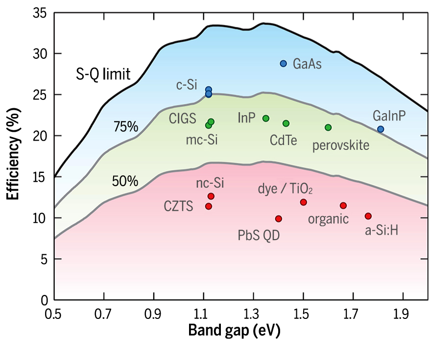
Theoretical Shockley-Queisser detailed-balance limit as a function of band gap (black line) and 75 % and 50 % of the limit (gray lines). The record efficiencies for different materials are plotted for the corresponding band gaps. Reprinted with permission of Polman A., et al. (2016).
The thin-film solar cell with a large market share is based on a-Si:H, which also forms an important research platform for light management studies. The advantages of a-Si:H based solar cells are its conformal growth, which creates many perspectives in combination with nanoscale approaches, and the possibility to form flexible solar cells. Unfortunately the efficiency of the a-Si:H thin-film solar cell did not improve much beyond 12 % for many years. The main reason is the abundant presence of defects which form recombination centres for the electrons and holes.
Although CdTe, and the chalcopyrite compound copper indium gallium diselenide (CIGS) are currently market products as thin-film solar cells (Miles R.W. et al., 2007), research is increasing the laboratory efficiency which makes them more attractive.
Perovskites are currently being very intensively investigated, and impressive laboratory efficiencies of up to 22.1 % have been reported (Fig. 2). Although the advantages of perovskites include ease of fabrication, strong solar absorption and low non-radiative carrier recombination rates, the instability under ambient conditions and illumination due to the presence of organic compounds hinders commercial success. Replacement of the organic components is an important goal which will bring this material to the market. The low resistance of present perovskite technology to moist air and water vapour together with the inability to produce high-quality large surfaces forms a serious bottleneck. Although perovskites can be used as a thin-film solar cell, they can also be used as a dye particle in, for example a TiO2 electrode.
In thick conventional crystalline silicon solar cells, light management techniques such as anti-reflection texture and coatings have been employed successfully for a long time. Because such an anti reflection texture has dimensions much larger than the thickness of thin-film solar cells they are not suitable. Therefore new light-trapping techniques at the nanoscale, which are compatible with the thin-film solar cell, have to be found (Brongersma M.L. et al., 2014; Chattopadhyay S. et al., 2010; Kuznetsov A.I. et al., 2016).
3.1 PlasmonicsPlasmonics, the electronic response of light interacting with metal nanostructures, is a promising novel concept in the quest for photovoltaic devices with high efficiencies and low-cost materials. The interest in plasmonics, which merges optics with electronics (Maier S.A. et al., 2001; Ozbay E., 2006) at very small scales, has increased considerably since about a decade. Five main effects are distinguished with the metal plasmon and optically active neighbouring materials (Maier S.A., 2007): 1) Plasmonic field enhancement (Atwater H.A. and Polman, 2010; Ferry V.E. et al., 2010; Pala R.A. et al., 2009; Pillai S. et al., 2007), (a near-field effect) increases the electromagnetic field close to the metal surface by orders of magnitude. This is the result of the (dipole) electric field around the metal nanoparticle in response to illumination. This is particularly interesting for thin-film solar cells as light concentration has a significant effect on the overall absorption. 2) Scattering at/by the metal nanoparticle (Bohren C.F. and Huffman, 2004) increases the light path length in a solar cell and is therefore an important mechanism to increase efficiency. Incident light is scattered off the metal object into a distribution of optical modes within the semiconductor. 3) Coupling of plasmon resonance to waveguide modes in thin semiconductor slabs. 4) The coupling of an (semiconductor) emitter to plasmon modes also affects both the radiative and non-radiative decay rates. This phenomenon is based on the principle that the strength with which an emitter couples with an electromagnetic field depends on its environment (Anger P. et al., 2006; Novotny L. and Hecht, 2006; Purcell E., 1946). 5) Energy transfer from the absorber/emitter to plasmon modes of a nearby nanoparticle or vice versa can occur by, for example Forster Energy Transfer (FRET) (Govorov A.O. et al., 2006). This energy will be partially dissipated or coupled to radiation (Clapp A.R. et al, 2006; Michalet X. et al., 2005). The balance between these effects depends strongly on the geometry, shape, size and distance (Haes A.J. et al., 2004). A schematic of some plasmonic interactions is shown in Fig. 4.
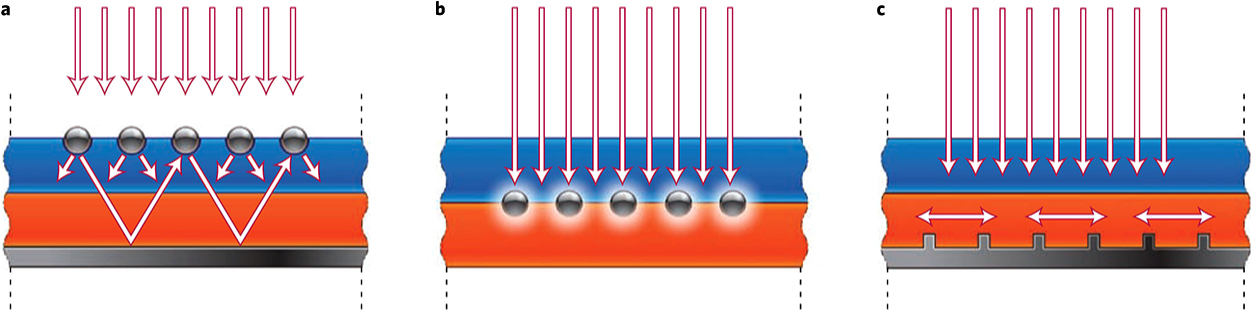
Plasmonic light-trapping geometries for thin-film solar cells. (a) Light trapping by scattering from metal nanoparticles at the surface of the solar cell. Light is preferentially scattered and trapped into the semiconductor thin film by multiple and high-angle scattering, causing an increase in the effective optical path length in the cell. (b) Light trapping by the excitation of localized surface plasmons in metal nanoparticles embedded in the semiconductor. The near-field of the excited particles causes the creation of electron–hole pairs in the semiconductor. (c) Light trapping by the excitation of surface plasmon polaritons at the metal/semiconductor interface. A corrugated metal back surface couples light to surface plasmon polariton or photonic modes that propagate in the plane of the semiconductor layer. Reprinted with permission of Atwater H.A. and Polman A. (2010).
One of the first experimental investigations of plasmonic enhancement for photovoltaics involved silver nanoparticles in an organic solar cell (Stenzel O. et al., 1995; Westphalen M. et al., 2000). The first papers to explore the potential of localized surface plasmon resonance (LSPR) in solid-state photovoltaics were published in the late 1990s by Stuart and Hall (Stuart H.R. and Hall, 1996). Their device consisted of a thin silicon-on-insulator wafer, where the Si was 165 nm thick, and since the absorbing Si layer was separated from the Si substrate by a layer of SiO2, it acts as a thin waveguide. Metal island formation was achieved by the deposition of a thin metallic film and annealing under N2 so that the film coalesced into discrete islands. Subsequent studies show that the local field enhancement and scattering of plasmonic nanostructures increases the solar cell performance (Atwater H.A. and Polman, 2010; Maier S. et al., 2001; Pala R.A. et al., 2009) (Ferry V.E. et al., 2010). Additionally, work by Barnard et al. (Barnard E.S. et al., 2011) shows the enhancing effect of silver nanostructures on the photocurrent in silicon. Underneath a metal nanoantenna, the field intensity is enhanced by a factor of 2.8 while locally, the field enhancement can be significantly higher (up to 20) in “hot spots” under the corners of the antenna. A theoretical study of plasmonic nanoparticles for solar cells shows that an absorption increase of 10–15 % is more than feasible (Akimov Y.A. et al., 2009).
To date, most research focused on noble metals (Hägglund C. et al., 2008; Nakayama K. et al., 2008) which have strong resonances in the visible part of the spectrum and have the advantage of being inert. However, the high price of noble metals makes them difficult for commercial solar cells. Although aluminium has its bulk plasmon resonance in the far UV range at around 150 nm, its plasmon resonance can be shifted, making it a cheap alternative. The plasmon resonance wavelength of aluminium nanoparticles can be shifted towards the visible range by selection of size, shape, configuration and dielectric environment (Ekinci Y. et al, 2008; Knight M.W. et al., 2012; Langhammer C. et al., 2008; Olson J. et al., 2014; Tan S.J. et al., 2014; Temple T.L. and Bagnall, 2011; van der Vliet T. and Di Vece, 2016). The electron collision frequency at a plasma frequency in the visible range in aluminium is in between that of gold and silver (Tassin P. et al., 2012), which make Ohmic losses acceptable. A theoretical study by Akimov at al. (Akimov Y.A. et al., 2009) has demonstrated that aluminium particles increase the optical absorption in a-Si:H over a wide wavelength range better than silver particles.
Nanoparticle plasmonics: although previous research on using plasmonics for solar cells included both nanoparticles and nanostructures formed by lithography as shown in Fig. 5, much work remains to be done as commercial applications are still not realized. Although lithography has been very rewarding as a proof of principle method, this top-down technique is economically not yet interesting. However, the roll-to-roll nano imprint lithography technique has been used in such studies and is industrially more interesting (Ferry V.E. et al., 2010; Kooy N. et al., 2014). The use of (plasmonic) nanoparticles from a bottom-up approach as demonstrated by Faraone G., et al. (2018) has many advantages such as speed and low cost, which brings these novel concepts within industrial reach.

Current–voltage characteristics of nanopatterned cells. The cells are conformally deposited over the patterned substrate, as shown schematically in (a) and in SEM cross-section in (b). The maximum particle diameter in the backpattern was chosen so that nanostructures in the ITO top layer would touch without overlap. (c) Current density–voltage measurements for the best-efficiency cells on the substrate with 90 nm intrinsic layers. The optimized periodic pattern and the pseudorandom pattern have efficiencies of 9.6 and 9.4 %, respectively. Reprinted with permission of Ferry V.E., et al. (2011).
A new approach to more efficiently coupling light into a thin-film solar cell is the use of Mie scatterers as shown in Fig. 6. In a Mie scatterer, usually a dielectric particle such as silicon (Spinelli P. and Polman, 2014) with the dimension of the wavelength of light (down to 10 %), the scattering of light often has a stronger intensity in the forward direction which is useful when a light absorbing material is placed beneath it. The forward scattering couples the light efficiently into the layers below it (Spinelli P. et al., 2012). Since a Mie scatterer is made out of a dielectric material and not a metal with electric resistance acting on the plasmonic resonance, its optical losses are minimal. When the Mie scatterer is large, the captured light will resonate at particular wavelengths, depending on the interference conditions, which enhances its optical cross-section for these wavelengths. The circulating light in this Mie scatterer can be coupled into a solar cell beneath it by leaking, which makes a more efficient and selective harvesting of light possible. Mie scattering can provide a broad-band optical absorption with, for example silicon nanocone arrays (Wang Z.Y. et al., 2015). The Mie scatterer is not limited to solar cells but can also be employed in solar fuel generation by light (Cheng Y.Y. et al., 2012; Kim S.J. et al., 2014). The Mie scatterer composition can be chosen to obtain the desired optical properties as shown by using silicon carbide (Schuller J.A. et al., 2007), silica (Nunomura S. et al., 2010) and germanium (Cao L. et al., 2010) particles.

Schematic showing how various optical resonances supported by a model cell structure can be excited to enhance light absorption in the active semiconductor material (green). The numbers 1–4 label four distinct coupling mechanisms. 1: Excitation of an optical (Mie) resonance of hexapolar symmetry in the NWs. This resonance is hybridized with a guided resonance in the underlying Si layer. 2: Fabry-Perot standing-wave resonance that results from the confinement of light between the reflecting top surface of the high-index Si film and the metallic back-reflector. 3: Guided resonance of the Si layer. 4: Excitation of diffracted modes. Such modes can be excited when incident light is redirected into the plane of the light-trapping layer, where they concentrate most of the field. These modes also extend into the underlying semiconductor layer where they can induce useful absorption. Reprinted with permission of Brongersma M.L., et al. (2014).
In most of the current research of Mie scatterers for solar cells, top-down techniques such as lithography and laser printing (Zywietz U. et al., 2014) are used to create the desired nanostructures. As this is commercially not yet attractive, alternative methods (i.e. bottom-up) to fabricate Mie scatterers for solar cells need to be explored. Although wet chemical techniques are used to fabricate Mie scattering structures (Araújo A. et al., 2017; Karg M. et al., 2015), more industrially compatible techniques are desirable. A recent work by (Giannakoudakis and Di Vece, 2017) shows that TiO2 Mie scatterers can be produced with a gas aggregation cluster source and combined with a-Si thin films. TiO2 has also been used as a Mie scattering composite in dye-sensitized solar cells (Son S. et al., 2013) and as a scatterer for solar cells (Kang S.H. et al., 2008). Since thin a-Si films are used in solar cells, they function as a photovoltaic model system. TiO2 Mie scatterers can easily be fabricated with a gas-phase aggregation cluster source (Barborini E. et al., 2003; Polonskyi O. et al., 2013), which is fast, cheap, vacuum-compatible and provides ultra-clean and well-defined particles. TiO2 particles were also produced by a pulsed microplasma cluster source (Barborini E. et al., 2003), which demonstrates its versatility.
3.3 Quantum dotsAlthough commercial quantum dot solar cells are not available (Jabbour G.E. and Doderer, 2010), the quantum-dot-based emitting displays (QDOT) (Dai X. et al., 2017) demonstrate that this could become reality in the near future. Most of the current solar cell materials are used or could be used in a thin-film design. The inspiration for quantum dot solar cells is the tandem or multi junction cells in which more photons of different energy are harvested. Although such solar cells are commercially available and indeed have a higher efficiency (Law D.C. et al., 2010), they are, however, very expensive, leaving ample space for research towards economically viable materials.
The band gap of a semiconductor can be changed by reducing the size, typically well below 10 nm (Nebel C.E. et al., 1998; Nozik A.J., 2002) due to quantum confinement as illustrated in Fig. 7. These quantum dots (Alivisatos A.P., 1996; Murray C.B. et al., 2000) allow the use of a single cheap semiconductor in a tandem solar cell. However, solar energy conversion to electricity in these quantum dot solar cells remains too low (below 10 % (Jabbour G.E. and Doderer, 2010)) and therefore requires fundamental improvements. One of the key factors is the efficient transport of charge carriers (electrons and holes) toward the opposing electrodes. The chemical properties of the quantum dot surface, the material between the quantum dots and the contact properties with the electrodes are all very important to obtain the best efficiency. One of the promising quantum dot compositions is PbS or PbSe, these are conveniently produced and have promising optical and electronic properties (Carey G.H. et al., 2015). A schematic of the different uses of quantum dots for solar cells is shown in Fig. 8.
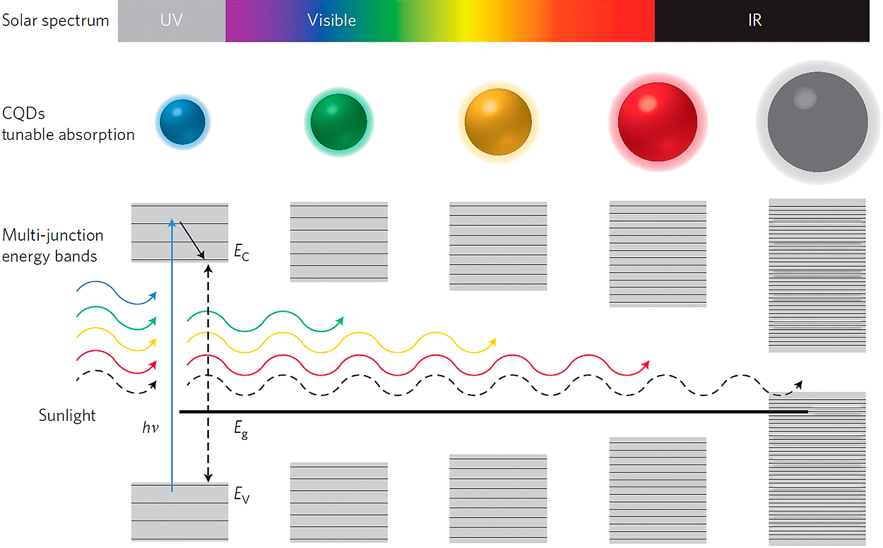
Size-dependent absorption enables QDs to be tuned to absorb, sequentially, the constituent bands making up the sun’s broad spectrum, paving the way for the construction of multi-junction solar cells that overcome the energy loss in single-junction cells resulting from thermalization. This is achieved by reducing the discrepancy between the energy of absorbed photons (hν) and the bandgap (e.g. dashed black arrow) of the material in which they are absorbed, so that the energy lost by the photoexcitations due to thermalization (solid black arrow) is minimized. EC and EV are the conduction and valence band edges, respectively. Reprinted with permission of Lan X. (2014).
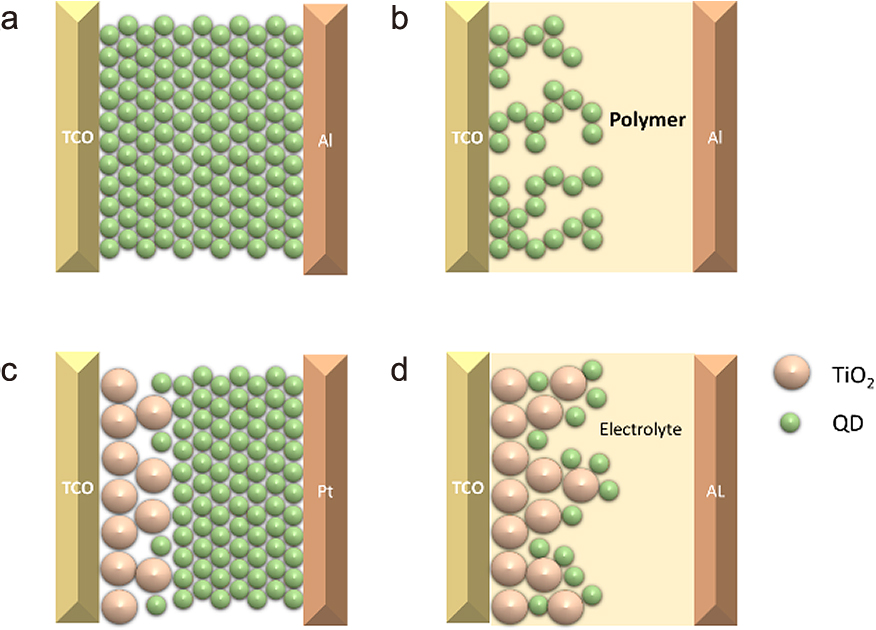
Different QD-based photovoltaic cells. (a) Schottky cell; (b) hybrid polymer solar cells; (c) heterojunction cell and (d) QD-sensitized solar cell.
Silicon QD: although new concepts and materials are intensively investigated to further increase efficiencies, the “old work horse” silicon remains a very attractive photovoltaics (PV) material. Silicon as a quantum dot may lead to enhanced device performance (Conibeer G., 2007). Besides the possibility of silicon quantum dots to tune their band gap (Cullis A.G. and Canham, 1991) which can be employed in a tandem cell, a direct band gap may appear for the smallest sizes (de Boer W.D.A.M. et al., 2010). In principle a direct band gap increases absorption as compared with the indirect band gap of bulk crystalline silicon (Prokofiev A.A. et al., 2010). However, small quantum dots have a low density of states which in turn reduces their optical absorption.
The photoluminescence of silicon nanoparticles yielded a clear size dependence of the luminescence emission energy due to quantum confinement (Delerue C. et al., 1998; Ledoux G. et al., 2000; Takeoka S. et al, 2000; Tekin E. et al., 2008; Wilson W.L. et al., 1993). Photoluminescence on silicon particles which were fabricated by laser ablation showed radiative decay lifetimes of microseconds at room temperature which also depends on size and the available phonon contribution (Watanabe K. et al., 2002). Multiple exciton generation in silicon nanoparticles was observed by a step-like enhancement of the luminescence quantum yield (Timmerman D. et al., 2011). In a work by Trinh et al. (Trinh M.T. et al., 2012), the direct generation of multiple excitons was even possible in adjacent silicon nanoparticles.
The main reason why currently silicon quantum dot research is not very active is the inability to produce silicon quantum dots by wet chemical means. Various methods to fabricate silicon particles for solar cells have been studied with proof of principle devices. From silicon-rich silicon oxide or silicon carbide, nanoparticles are formed upon annealing whereby the silicon atoms aggregate to form particles (Conibeer G. et al., 2006). A similar process is possible by Si ion implantation (Shimizu-Iwayama T. et al., 1998). However, these silicon nanoparticles have a large size distribution and are often separated by large distances, which hinders electrical conductance. The large size distribution will prevent accurate tuning of the band gap and forms exciton-trapping centres. The fabrication of monodisperse silicon quantum dots with controllable separation distance is a prerequisite for successful application in a solar cell. Work by Mohan et al. (Mohan A. et al., 2017) shows that it is possible to obtain silicon nanoparticles by using a pulsed SiH4/Ar plasma. In a recent work by Tang et al. (Tang W. et al., 2015), the silicon nanoparticles were fabricated with a gas aggregation cluster source, which is a promising route.
3.4 Spectral budgetingPhotons having an energy higher than twice that of the band gap (i.e. in the 280–400 nm spectral range) do not contribute efficiently to the energy conversion. To reduce the losses, photon conversion concepts have been proposed: down-shifting (where an ultraviolet (UV) photon is converted into a visible or infrared (IR) photon) (Hovel H.J. et al., 1979) and down-conversion (a UV photon is converted into two visible or IR photons) (Richards B.S., 2006; Trupke T. et al., 2002). Down-conversion is also often called singlet exciton fission (Lee J. et al., 2013). The advantage of down-shifting is that the reduced photon energy enables the photon to penetrate deeper into the active semiconductor layer while for down-conversion, the two photons are better absorbed. A schematic image to illustrate up- and down-conversion for a solar cell is shown in Fig. 9. To date, down-shifting and down-conversion have not led to significant improvements, and better systems need to be developed (Fix T. et al., 2015). Luminescence provides a good way to down-shift the photon (Švrček V. et al., 2004; van Sark W. G.J.H.M. et al., 2004).

Spectral conversion design for PV applications involving down-shifting (DS), quantum-cutting (QC), and upconversion (UC) of luminescent materials. In a typical downshifting process, upon excitation with a high-energy photon, non-radiative relaxation takes place followed by radiative relaxation, thereby resulting in the emission of a lower-energy photon. In contrast, two-step radiative relaxation occurs in the quantum-cutting process upon excitation with a high-energy photon, leading to the emission of two (or more) lower-energy photons. The upconversion process can convert two (or more) incident low-energy photons into a single higher-energy photon. The downshifting and quantum-cutting materials are generally placed on the front surface of a monofacial solar cell, allowing the downconverted photons to be absorbed by the solar cell. The upconversion material is typically placed in between a bifacial solar cell and a light-reflection layer to harvest the sub-bandgap spectrum of sunlight. Reprinted with permission of Huang X. (2013).
Alternatively, the up-shifting (up-conversion) of IR photons, which means that multiple IR photons will be harvested by a nanoparticle and converted into a single photon in the visible range, can be used to increase the efficiency of a solar cell (Bloembergen N., 1959; De Wild J. et al., 2013). The commercially available up-converter, Gd2O2S:Yb3+, Er3+, in which Yb3+absorbs light around 980 nm and Er3+ emits in the visible spectrum (400 to 700 nm) needs to be improved (de Wild J. et al., 2011; Haase M. and Schafer, 2011). For example, with nanocrystals of NaYF4:Er3+, Yb3+ also shows up-conversion. An advantage of using nanocrystals is that transparent solutions or transparent matrices with up-converting nanocrystals can be obtained.
3.5 Nanoparticles as a constituentMany of the thin-film solar cells can also be fabricated by using nanoparticles as a constituent (Stolle C.J. et al., 2013). The dye-sensitized solar cells are famous and use TiO2 particles as (dye) support (Gratzel M., 2001). Although the technology can be cheap, the dyes are often unstable in sunlight and the presence of electrolytes makes it difficult to handle and seal. Additionally, the efficiencies have not surpassed 12 % during the last two decades of research. Nanoparticle precursors are used to fabricate CIGS (Kapur V.K. et al., 2003), CZTS (Lokhande A.C. et al., 2016) and CdTe (Anderson I.E. et al., 2009) solar cells. The particles are fabricated by wet chemical procedures and deposited from solution by spin-coating, ink-jet printing or spraying. The advantage is the relatively uncomplicated technique and the low temperatures. The disadvantages are the lack of crystallinity and presence of contaminants.
Colloidal nanoparticles have the advantage of large-volume production and ease of deposition by, for example, spin coating or electro spray. The main disadvantages are the stabilising chemicals in the solutions which form a source of contamination and some (crystalline) compositions are not easily synthesised by wet chemistry. The diverse fabrication methods of solar cells provide many opportunities for the different nanoparticle fabrication techniques. Thin-film a-Si:H is grown by plasma-enhanced chemical vapour deposition (PE-CVD) from Siand H-containing precursors (Schropp R.E.I., 2015). Conductive electrodes and anti-reflection coatings are also applied in a vacuum environment. This makes physical deposition of particles with cluster sources very attractive. An example of embedding silver nanoparticles inside a-Si:H solar cells is given in Fig. 10. Although the reactor chamber of a cluster source can be at about 10−1 mbar, the deposition pressures of gas aggregation cluster sources are between 10−5 and 10−8 mbar, which leaves the solar cell (parts) undisturbed as the presence of reactive gaseous species is minimal. Along with the nanoparticles, a carrier gas is transported to the deposition chamber, usually argon and/or helium, both of which are noble gasses and therefore do not contaminate the solar cell.
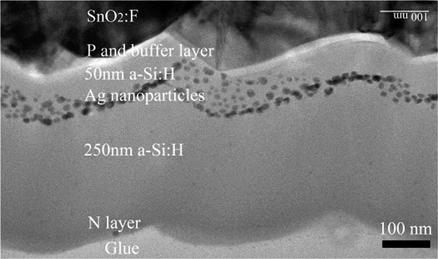
TEM cross-section of an a-Si:H solar cell with silver nanoparticles embedded at a depth of 50 nm in the absorber layer. Reprinted with permission of Santbergen R. (2010).
Various cluster sources would be suitable for the fabrication of nanoparticles for PV. The different types of cluster sources are well described in literature (de Heer W.A., 1993; Popok V.N. et al., 2011; Wegner K. et al., 2006b). In the gas-aggregation source, metal is vaporized and introduced in a flow of cold inert gas. This causes the vapour to become highly supersaturated. Due to the low temperature of the inert gas, cluster production proceeds primarily by successive single-atom addition. The cluster size distribution is determined by the parameters of the source such as the metal-vapour density, gas flow rate, and dimensions of the various components. Gas-phase cluster sources work in either pulsed or continuous mode, both of which are suitable for optical layers. The term “cluster source” is slightly confusing as in the past, the device was often used to study few atom particles. Since many cluster sources are capable of producing nanoparticles of up to tens of nm, a new name would be appropriate.
The seeded supersonic nozzle source (SSNS) and the thermal gas aggregation source (TGAS) use thermal evaporation to produce nanoparticles at high yield, but is limited to the metals. The sputter gas aggregation source (SGAS) uses sputtering to replace Joule heating to vaporize the material. The strong advantage of this method is that any solid can be used: metals, semiconductors and insulators. In Fig. 11, silicon nanocrystals made with such a cluster source are shown. The laser ablation source (LAS) also has the advantage of being able to ablate most solids and having a high yield. However, only small particles can be produced. Pulsed-arc cluster ion sources (PACIS) use an arc discharge between two metallic electrodes in combination with an inert gas burst. The yield is high but oxide particles can only be produced by the oxidation of metal particles, which is too complicated and time-consuming for optical coatings on semiconductor surfaces. Additionally, the particle sizes are very small. The pulsed microplasma cluster source (PMCS) combines the LAS and PACIS, resulting in high particle fluxes. However, only metal or highly doped semiconductor nanoparticles can be produced.

TEM image showing the general morphology of the Si nanoparticles produced by a magnetron sputtering cluster source and the inset is the selected area electron diffraction pattern. Reprinted with permission of Wang L. (2008).
Cluster sources are excellently suited for producing light management structures with metal and dielectric particles. The particles can be deposited at any stage of the solar cell fabrication and the random distribution of particles may be advantageous. The most promising cluster source is the magnetron sputtering gas aggregation cluster source, which has the main advantage of being able to use all materials (metal, semiconductors and insulators). The main disadvantage is the production of excess material that deposits in the reactor chamber and which needs to be cleaned regularly. The magnetron sputter cluster source was developed by Haberland (Haberland H. et al., 1994) (Fig. 12a), and is now one of the few cluster sources which is commercially available (“Mantis”, “Oxford Applied Research Inc.”). Magnetron sputter cluster sources with multiple targets are currently also available which make it possible to produce complicated alloy or core shell nanoparticles.

Production of size-selected cluster beams. (a) Cluster formation by plasma sputtering and gas aggregation. (b) Overview of the complete cluster beam source. (c) Mass spectra of Ag clusters produced by the source. Reprinted with permission of Palmer R.E., et al. (2003).
The nanoparticle sizes from these cluster sources range from a few atoms to about 100 nm. The latter can usually be obtained using magnetron sputtering with a large aggregation distance. Considering, for example the Bohr radius of silicon and germanium, this allows the fabrication of quantum dots. With respect to plasmonic and Mie particles, this is clearly within range and compatible with thin-film solar cell dimensions. Complicated compositions such as perovskite particles are difficult to produce with gas aggregation cluster sources although multiple target magnetron sputtering is promising in this respect. A recent work by Palmer et al. demonstrates a high yield cluster source with the launch of a new type of cluster production: the “Matrix Assembly Cluster Source” (Palmer R.E. et al., 2016), in which large quantities of clusters are produced by use of an Ar matrix in which the cluster atoms aggregate and are subsequently sputtered out. Since the output has increased from nanoamps (in conventional cluster sources) to milliamps, this is indeed promising for industrial applications.
The mass selection of nanoparticles from a cluster source can be achieved by magnetic deflection (Gerlach W. and Stern, 1922), time of flight (de Heer W.A. and Milani, 1991; von Issendorff B. and Palmer, 1999), quadrupole mass filter (Paul W. and Steinwedel H., 2014), aerodynamic lenses (Piseri P. et al., 2004), the Wien filter (Wien W., 1902) and the magnetic sector. Although the disadvantage of all these systems is the loss of most of the particles produced by the cluster source and therefore a smaller amount will be deposited, the particle size can be easily tuned for optical purposes such as plasmonics or quantum dots. With some mass selectors, monolayers can be obtained in reasonable deposition times, such as the time of flight and quadrupole. This will often be good enough for light management structures. However, many cluster sources have a size distribution in the order of 10–20 % which is already sufficient for optical nanostructures. This does away with the necessity of a mass selector and increases the deposition time considerably. An example of a magnetron sputtering gas aggregation cluster source with time-of-flight mass selector is shown in Fig. 12b.
A laboratory gas aggregation cluster source can produce a monolayer of metal, insulator or semiconductor particles within about a minute. Up-scaling would increase this speed and enable the coverage of large areas. The produced nanoparticles are ultra clean and are therefore compatible with any solar cell fabrication stage. The easy and quick control over particle size, often by tuning parameters such as magnetron/laser power, gas flow and aggregation distance, provides versatility with respect to the desired configuration. The magnetron gas aggregation cluster source has the advantage of being able to produce metal, semiconductor and insulating particles by DC or RF sputtering. The nanoparticles from magnetron cluster sources are often highly crystalline, which is important for the plasmonic particles, Mie scatterers and quantum dots. Because the nanoparticle quantity required for solar cell applications ranges from sub-monolayers to about 50 monolayers, it is within the reach of most cluster sources. For example, silicon and germanium quantum dots have been very hard to fabricate with chemical methods, which provided limited research results. With gas aggregation cluster sources, it is possible to produce such quantum dots in optically thick layers. The formation of patterns made out of nanoparticles by using a hard mask may prove very useful to apply structures in the photovoltaic device (Wegner K. et al., 2006a). It is clear that this provides many research opportunities.
4.2 Colloidal depositionThe colloidal deposition techniques are currently routinely used and could be easily up-scaled. The spin-coating of nanoparticles is probably the simplest method to deposit nanoparticles. For applying light management structures on solar cells, it has the disadvantage that the solution often interacts with the delicate solar cell surface, the solar cell needs to be exposed to the ambient and the size is limited due to the rotational motion. Spin-coating and layer-by-layer exchange lead to vast material waste: typically only 1–10 % of the consumed quantum dots are incorporated into the final film (Ning Z. et al., 2014). (Electro-) Spraying is a promising alternative which can cover very large scales reliably (Kramer I.J. et al., 2015; Salata O.V., 2005). The droplets containing particles are deposited on the desired substrate, after which the solvent evaporates. Although some molecules from the solution are also deposited, they may be able to evaporate or are considered to be harmless. A new development is the inkjet deposition of colloidal quantum dots (Tekin E. et al., 2008), which even allows the creation of structures in the layers (Fischer A. et al., 2013; Kirmani A.R. et al., 2014). An example of a working solar cell produced by ink deposition is shown in Fig. 13.
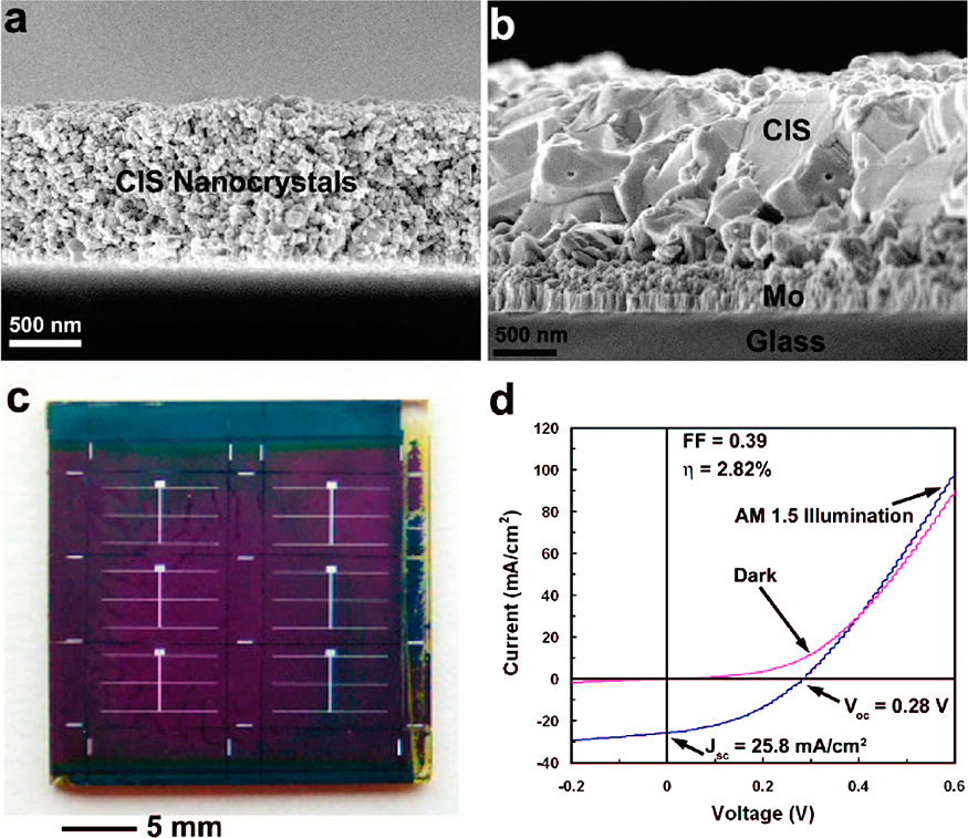
CuInSe2 solar cells fabricated from a nanocrystal ink. FESEM images of (a) CuInSe2 nanocrystal thin film after casting and (b) after sintering in a Se/Ar atmosphere. (c) A photograph of the completed solar cells after chemical bath deposition of CdS, sputtering of i-ZnO and ITO, and evaporation of metal contacts. (d) The I–V characteristic of the finished device. Reprinted with permission of Guo Q. (2008).
A promising route by employing colloids is the aerosol deposition technique. The aerosol, in this case a liquid droplet containing the colloid particles, is sprayed on to the surface of interest, depositing metal, semiconductor and insulating nanoparticles (Gurav A. et al., 1993; Noor N. and Parkin, 2013; Palgrave R.G. and Parkin, 2006). Ultra-porous TiO2 layers for perovskite solar cells are made by the flame pyrolysis of aerosols (Mayon Y.O., et al., 2016).
Colloidal particles have to be deposited from solutions, which makes it compatible with solar cell materials such as CIGS (Choi K.-H. et al., 2011), Perovskites or quantum dot solar cells. Both CIGS and CZTS solar cells can be fabricated by colloidal deposition (Akhavan V.A. et al., 2012). However, the solvents are often toxic and may not be compatible with vacuum techniques and reduce the possibility to hybridise the fabrication.
Different scientific disciplines are often well separated and it is therefore important to create bridges between them, of which this review paper is an attempt. The photovoltaic community, including the novel concept work, is in general not familiar with nanoparticle research and vice versa. As described above, there are many aspects of novel concept solar cell development in which nanoparticles can play an important role. This is particularly interesting with respect to industrial feasibility, in contrast to lithographic techniques, which currently are limited to the proof of concept designs.
Two main nanoparticle and solar cell fabrication techniques can be distinguished: 1) the physical fabrication/deposition which often makes use of vacuum techniques, and 2) the chemical fabrication/deposition which involves the presence of liquids and is not necessarily compatible with physical fabrication/deposition. In contrast to conventional wafer-based solar cells, these fabrication processes can be performed at room temperature, which reduces the fabrication cost considerably.
The integration of cluster sources with research fields such as solar cells is currently not far beyond its conception. The maturation of using cluster sources for photovoltaics lies in the near future, which is stimulated by the commercial availability of gas aggregation cluster sources.
It is likely that nanoparticles will find their way into photovoltaics by different techniques and approaches. Light management remains interesting to increase the efficiency of thin-film solar cells for many years to come. The different compositions of thin-film solar cells, including the promising perovskites, will provide decades of research possibilities for nanoparticle implementation. From an industrial point of view, nanoparticles are cheap to produce and easy to combine with existing fabrication methods in PV technology. Not only do the separate scientific communities of PV and nanoparticles have to cross-fertilize, their industrial counterparts may significantly benefit from such an approach.
Using nanoparticles for photovoltaics is a promising bottom-up approach for various aspects of the thin-film solar cell. The nanoparticles can be used as a constituent such as CIGS or perovskite or as a quantum dot. Particularly the “traditional” materials such as silicon and GaAs are waiting for new fabrication techniques to be employed as quantum dots in solar cells. The nanoparticles can also be used as a light management structure in or on thin-film solar cells. Plasmonic particles can scatter light or the local field enhancement can increase absorption. Dielectric Mie scatterers can also scatter light or can function as light antennas to subsequently couple light into the active solar cell layer. Photon up- and down-conversion materials can also be fabricated as nanoparticles. Although wet chemical techniques can produce nanoparticles in large quantities, the disadvantage is the presence of unwanted chemicals from the fabrication procedure and a lack of crystallinity. Moreover, some compositions such as silicon and germanium turn out to be very difficult to fabricate chemically in the form of nanoparticles. The gas aggregation cluster source is proposed here as new fabrication technique for nanoparticles covering the compositional and light management parts in thin-film solar cells. Because thin-film solar cells require only one or several monolayers of particles, this is feasible. By merging two historically independent research fields, a bright future for nanoparticles and solar cells is on the horizon.
Discussions with Prof. Dr. Ruud E.I. Schropp are very much appreciated.
Cadmium telluride
CIGSCopper indium gallium (di)selenide
CZTSCopper zinc tin sulfide
FESEMField Emission Scanning Electron Microscopy
LASLaser ablation source
PACISPulsed-arc cluster ion sources
PE-CVDPlasma-enhanced chemical vapour deposition
PMCSPulsed microplasma cluster source
PVPhotovoltaics
QDQuantum dot
SGASSputter gas aggregation source
SQShockley-Queisser
SSNSSupersonic nozzle source
TEMTransmission electron microscopy
TGASThermal gas aggregation source
Marcel Di Vece
;%0A%09%09%09newWindow.document.open();%0A%09%09%09newWindow.document.write('<img src=%22./Graphics/36_2019005_14.jpg%22>');%0A%09%09%09newWindow.document.close();%0A%09%09)
Marcel Di Vece is currently affiliated with CIMAINA and the Department of Physics at the University of Milan, Italy. He obtained his PhD at Utrecht University (Netherlands) in 2003 on the “Switchable mirror”. Since 2003, he has been working on various topics related to nanoparticles fabricated with gas aggregation sources. Since 2010, he has combined nanoparticles from a magnetron sputter nanoparticle source with thin films to investigate their potential for solar cells.