1. Introduction
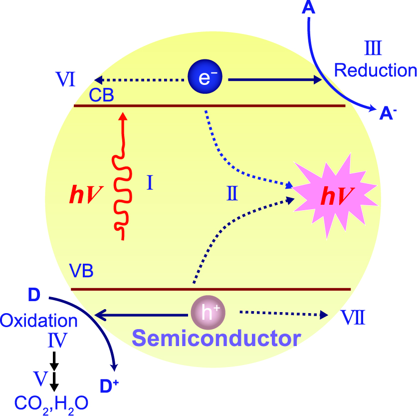
The Earth’s surface (i.e., the land and oceans) receives about 89 petawatts (PW = 1015 W) of solar energy from the total incoming solar radiation (Tian Y. and Zhao C.Y., 2013). This enormous sustainable energy has stimulated numerous applications, such as solar desalination, solar thermal electricity, and photocatalysis, to mitigate environmental deterioration and energy crisis. Among these strategies, semiconductor-based heterogeneous catalysis by harnessing solar energy, that is, the so-called photocatalysis, has drawn extensive attention since the first demonstration of photocatalytic water splitting by Fujishima and Honda in 1972 (Fujishima A. and Honda K., 1972). The fundamental mechanisms of the semiconductor-based photocatalysis have been widely explored and established by prior studies (Fujishima A. et al., 2008; Hoffmann M.R. et al., 1995; Linsebigler A.L. et al., 1995; Schneider J. et al., 2014). As schematically illustrated in Fig. 1 (Wang H. et al., 2014), a typical process of the semiconductor-based photocatalysis is composed of several steps, including light absorption, charge generation, separation and migration, and redox reactions. Initially, the photons, with energy equal to or exceeding the bandgap energy of the semiconductors, induce the generation and separation of electron-hole (e−-h+) pairs, where electrons are excited to the conduction band (CB), leaving holes in the valence band (VB). Subsequently, the electrons and holes migrate to the semiconductor surface and act as reductants and oxidants, respectively. The whole process is completed at very short time scales. Taking TiO2 as an example, the characteristic times for the charge carriers’ generation, migration, and interfacial charge transfer are at the time scales of femtoseconds, femtoseconds to picoseconds, and picoseconds to microseconds, respectively (Schneider J. et al., 2014).
The photocatalysis, however, still suffers from low efficiencies, resulting from several factors, including limited light absorption, inefficient molecule adsorption, and fast recombination of photo-induced charge carriers. To enhance the efficiency, a myriad of efforts have been devoted, such as creating photocatalysts by combining semiconductors with other functional materials (e.g., metals, metal oxides, graphene, and metal-organic frameworks (MOFs)). For instance, the formation of semiconductor heterojunctions, such as CdS/WO3 (Jin J. et al., 2015), Fe2O3/Cu2O (Wang J.-C. et al., 2015), CdS/C3N4 (Cao S.-W. et al., 2013), ZnO/CuO (Wang W.N. et al., 2015), and TiO2/Cu2O (He X. and Wang W.N., 2018), can enhance the light absorption and facilitate the charge separation. The enhanced charge separation can also be achieved by creating the semiconductor/graphene composites (Jiang Y. et al., 2014; Li N. et al., 2011; Nie Y. et al., 2016; Wang W.N. et al., 2014). While the incorporation of MOFs with semiconductors can improve the molecular adsorption (He X. et al., 2017a; He X. et al., 2017b). Given the aforementioned benefits of the formed semiconductor-based composite photocatalysts, a variety of methods have been applied, such as in situ growth (Cao S.-W. et al., 2013; He X. et al., 2017b; Wang D. et al., 2018a), and chemical precipitation (Huang H. et al., 2015; Huang L. et al., 2009). It should be noted that, complicated steps and long reaction durations are inevitable in these methods.
On the other hand, a microdroplet-based aerosol process (i.e., the spray process, hereafter) is an alternative approach for the facile and fast synthesis of semiconductor-based photocatalysts. In a typical spray process, microdroplets serve as the reactors, which produce materials with controllable stoichiometry, tunable size, and high crystallinity in a fast manner (Okuyama K. and Wuled Lenggoro I., 2003; Wang W.N. et al., 2011a, 2013), offering lots of opportunities to improve the efficiency of catalysts. Given the growing studies regarding the design of semiconductor-based photocatalysts via microdroplets during the past years, it is of great importance to summarize the progress on this subject, which would promote the future development of photocatalysts and their applications to address energy and environmental issues. Therefore, a comprehensive review is provided here, covering the basics of the spray processes and the utilization of these processes for the rational design and facile synthesis of efficient photocatalysts, including semiconductor heterojunctions, graphene/semiconductor composites, and MOF/semiconductor composites.
2. Basics of the spray processes
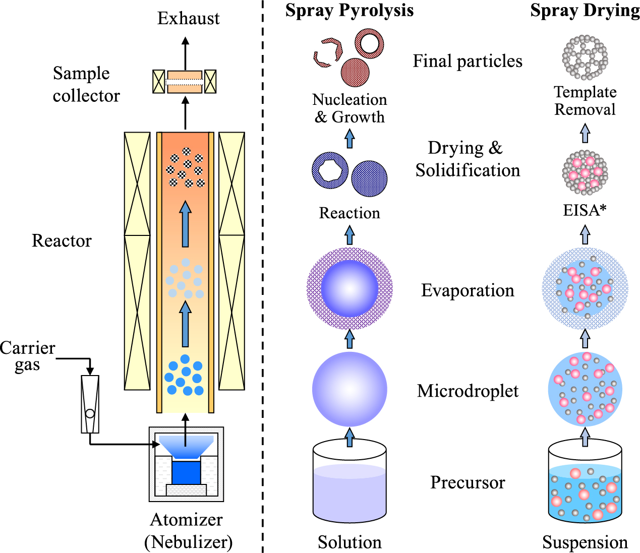
A schematic illustration of a representative spray system for the synthesis of nanomaterials is shown in Fig. 2. The system generally comprises of an atomizer (or nebulizer), an aerosol reactor, and a sample collector. In a spray pyrolysis process, the atomizer produces microdroplets from the precursor solution. The microdroplets are then fed through the aerosol reactor (e.g., an electrical furnace, a flame reactor, or a plasma chamber) by the carrier gas, where the solvent evaporation, nucleation, pyrolysis, and crystallization occur to form the final products (Wang W.N. et al., 2011a). In a spray drying process, a colloidal suspension is used as the precursor and the evaporation-induced self-assembly (EISA) of the colloids inside the microdroplets (Boissiere C. et al., 2011; Iskandar F. et al., 2003; Lu Y.F. et al., 1999) is a major step to form the final particles. Finally, the products are collected by the collectors, such as filters and electrostatic precipitators.
Theoretical understanding of mass and heat transfer principles within the microdroplets is of paramount importance to guide the design and synthesis of materials by using the spray process. For example, great attention has been attracted to the design of functional materials via the EISA of nanoparticles within microdroplets by manipulating the solvent evaporation rate of the droplets (Boissiere C. et al., 2011; Iskandar F. et al., 2003; Lu Y.F. et al., 1999; Wang W.N. et al., 2011b). Practically, two key parameters, i.e., the size and temperature of the microdroplets play significant roles in the droplet-to-particle conversion process. Their dependence on time is governed by the equations as shown below:
In continuum regime (i.e., the Knudsen number, Kn << 1): (Xiong Y. and Kodas T.T., 1993)
|
d
R
d
d
t
=
D
v
·
m
R
d
·
ρ
(
n
∞
-
n
s
)
| (1) |
|
d
T
d
d
t
=
3
c
p
R
d
[
H
vap
d
R
d
d
t
+
k
a
ρ
R
d
(
T
c
-
T
d
)
]
| (2) |
In free molecular regime (i.e., Kn >> 1): (Fisenko S.P. et al., 2006)
|
d
R
d
d
t
=
m
ρ
[
p
v
2
π
m
k
T
c
-
p
s
2
π
m
k
T
d
]
| (3) |
where Rd is the radius of the microdroplet; t is time; Dv indicates the diffusion coefficient of solvent vapor in air; m is the molecule mass of the solvent; ρ represents the solvent density; n∞ and ns denote the number densities of solvent molecules at the infinite region and droplet surface, respectively; Td and Tc are the temperatures of the droplet and the carrier gas, respectively; cp and Hvap are the specific heat capacity and the specific latent heat of the solvent, respectively; ka is the heat conductivity of air; k is the Boltzmann constant; pv and ps are the partial and saturated pressures of the solvent, respectively; p is the pressure of the carrier gas.
Several precursor and process parameters, including precursor concentration, viscosity, surface tension, droplet size, reactor pressure, temperature, and residence time, can be adjusted to control the properties of the final products (Hidayat D. et al., 2010; Wang W.N. et al., 2011a). For instance, the particle size is highly correlated with the concentration of the precursor solution (Nandiyanto A.B.D. et al., 2008). A governing equation describing this relationship has been developed based on the law of mass conservation (Iskandar F. et al., 2009; Wang W.N. et al., 2007; 2008; 2011b),
|
d
T
d
d
t
=
3
·
[
p
v
(
c
p
T
c
+
H
vap
+
0.5
k
T
c
)
m
T
c
-
p
s
(
c
p
T
d
+
H
vap
+
0.5
k
T
d
)
m
T
d
+
p
T
c
(
c
p
+
0.5
k
)
m
T
c
-
p
T
d
(
c
p
+
0.5
k
)
m
T
d
]
c
p
ρ
R
d
2
π
k
-
3
T
d
R
d
d
R
d
d
t
| (4) |
|
D
p
=
D
d
(
1
(
1
-
ɛ
)
∑
M
i
C
i
ρ
i
)
1
3
| (5) |
where the Dp and Dd are the volume mean diameters of the particles and droplets, respectively; M, C and ρ indicate the molecular weight, concentration and density of components in the precursor solution, respectively; ɛ represents the porosity of the final particles. In a conventional spray process, a high precursor concentration usually results in a larger particle size.
The pressure also has a significant effect on the properties of the products. At ambient pressure, a conventional spray process follows a one-droplet-to-one-particle (ODOP) principle, which can only generate large particles (i.e., ~ micrometers) due to the limitation of the fine droplet formation (Wang W.N. et al., 2011a). On the other hand, reducing the gas pressure inside the tube furnace reactor (i.e., low-pressure spray process) can significantly fasten the evaporation of the solvents and thus the nucleation of the products (Ashgriz N., 2011; Wang W.N. et al., 2011c). Besides, the low-pressure environment can also limit the aggregation of the products. Therefore, the low-pressure spray process usually produces much smaller particles (< 1 μm), following a one-droplet-to-multiple-particles (ODMP) principle (Ashgriz N., 2011; Hidayat D. et al., 2010; Wang W.N. et al., 2004; 2011a).
3. Design of photocatalysts via microdroplets
Based on the fundamental understanding of the spray process, various semiconductor-based photocatalysts have been designed via microdroplets, including semiconductor heterojunctions, graphene/semiconductor composites, and MOF/semiconductor composites.
3.1. Semiconductor heterojunctions
As mentioned above, the photocatalytic efficiency of semiconductors can be improved by combining the semiconductors with metals or other semiconductors to form heterojunctions, where the photoexcited charge carriers can be efficiently separated and migrated due to the built-in potential (Kittel C., 2005; Somorjai G.A. and Li Y., 2010; Wang D. et al., 2018b). The doped metals typically have three functions in the enhancement, including (1) reducing the over-potential as cocatalysts, (2) promoting the separation of charge carriers by creating an electric field near the interface, and (3) increasing light absorption of semiconductors with plasmonic effect (Qu Y. and Duan X., 2013).
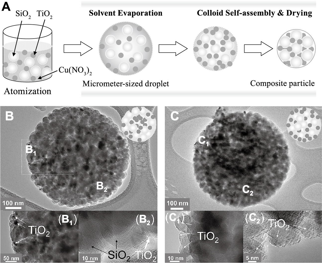
A large number of metal/semiconductor hybrid photocatalysts have been designed by using the spray pyrolysis process. In a typical synthesis procedure (Fig. 3), a mixture of metal ions and semiconductors are atomized to generate microdroplets. The microdroplets then pass through the reactor, where the metal ions are thermally reduced to metals and creating metal/semiconductor composite. For instance, a Pt/TiO2 hybrid was directly synthesized by a single-step flame spray pyrolysis (Teoh W.Y. et al., 2005). The size of Pt can be adjusted by varying the concentration of the Pt precursor. The results show that the incorporation of Pt affects not only the crystallinity and surface area of TiO2, but also the overall photocatalytic performance. The flame spray pyrolysis was also applied to synthesize noble metal/ZnO composites (e.g., Au/ZnO and Pt/ZnO) in one step (Pawinrat P. et al., 2009). The noble metals were homogeneously dispersed with average size between 3 and 7 nm. Species of the incorporated noble metals have significant effects on the photocatalytic activity. To be specific, the incorporation of Au can retard the recombination of charge carriers by modifying the Fermi level and trapping electrons. While, in the case of Pt, the electrons might be discharged into electrolytes. Similarly, Haugen et al. applied the spray pyrolysis technique to directly prepare metal (i.e., Ag and Au) doped TiO2 photocatalysts (Haugen A.B. et al., 2011). The incorporated metals were found homogeneously distributed within the composite. The as-prepared composites exhibit promising performance in photodegradation of environmental pollutants. Zhao et al. designed Ag/TiO2 composite photocatalysts by using an ultrasonic spray pyrolysis route (Zhao C. et al., 2012). The as-synthesized composite showed better dispersion of Ag, larger surface area, and thus a six-fold improvement in hydrogen production, in comparison to the one prepared by using the conventional wet-impregnation method. Recently, continuous spray pyrolysis was also applied to synthesize Au/CdS composite nanoparticles by using cadmium acetate, thiourea and chloroauric acid as the precursors (Kumar N. et al., 2014). The entire process is simple, fast and free of surfactants. The as-prepared hybrid nanoparticles exhibited enhanced photocatalytic efficiency as compared with bare CdS, which was mainly attributed to interfacial charge transfer as evidenced by the photoluminescence study. In addition, a Pt/WO3 composite photocatalyst was designed by Okuyama’s group (Widiyandari H. et al., 2012), where the existence of Pt could be indicated from the stacking-fault in the high resolution transmission electron microscopy (HR-TEM) image. The Pt in the composite acted as a capturer to snatch the photo-induced electrons and thus promotes the separation of the charge carriers. Another example of template-free synthesis of mesoporous Cu-TiO2-SiO2 nanocomposites by means of a spray route was demonstrated by Wang et al. (Wang W.N. et al., 2011b). As schematically shown in Fig. 4A, the nanocomposites were prepared from the aqueous suspensions of nanosized TiO2 and SiO2 colloids and copper nitrate via EISA. The particle size, composition, structure, and hence the catalytic performance were tailored by manipulating precursor properties and process parameters. For example, the reactor temperature was adjusted to control the solvent evaporation rate and hence the movement of TiO2 nanocrystals within the microdroplets. As shown in Figs. 4B and C, more TiO2 nanocrystals can be allocated on the surface of the nanocomposites by increasing the reactor temperature, resulting in enhanced catalytic performance. The self-assembly of the nanoparticles within the microdroplets was considered due to the thermophoretic force (Iskandar F. et al., 2003) and the Brownian motion (Hinds W.C., 1999). The thermophoretic force was created by the temperature gradient at the droplet surface, stemmed from the large heat transfer from droplet surface to gas stream due to the fast solvent evaporation.

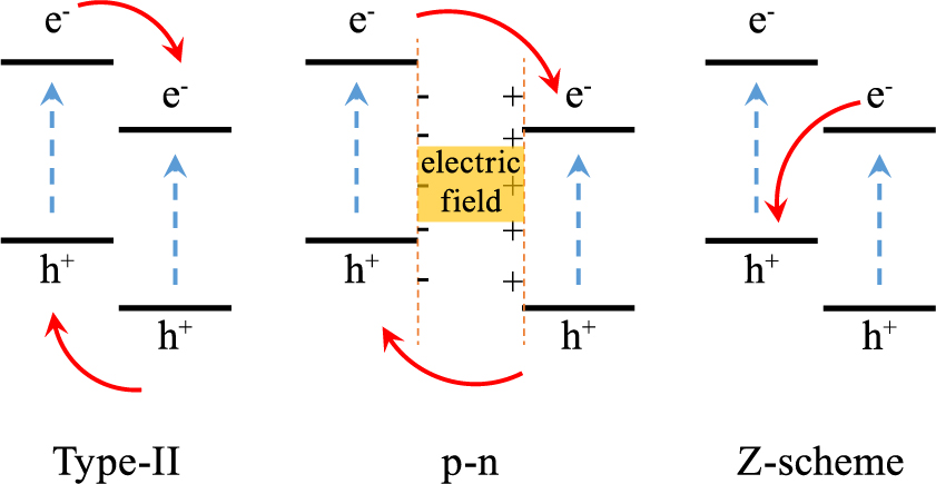
Regarding the semiconductor/semiconductor (SS) heterojunctions, the photocatalytic efficiency is mainly facilitated by the migration of charge carriers. The migration pathways at the interfaces are highly dependent on the band structures of the components. Representative types of SS heterojunctions are summarized in Fig. 5, including type-II, p-n, and Z-scheme. Detailed discussion of the charge transfer with different heterojunctions has been comprehensively documented in a recent review (Low J. et al., 2017). Therefore, only a brief explanation for each heterojunction is presented here. In the case of type-II heterojunctions, with the staggered gap, the electrons are confined to the one component semiconductor, while the holes are confined to the other one (Zhou H. et al., 2012). This produces spatially localized charges and promotes separation of charge carriers and thus the photocatalytic efficiency. The migration of the charge carriers can be further accelerated with p-n heterojunctions created by p-type and n-type semiconductors. The accelerated charge separation is mainly due to the additional interfacial electric filed, generated by the initial diffusion of electrons and holes (He Z. et al., 2014). It should be noted that, the redox abilities of both type-II and p-n heterojunctions are decreased due to the migration of the charge carriers to lower redox potentials. One solution to this issue is to form Z-scheme heterojunctions, where the photo-generated electrons with lower reduction potential migrate to the other semiconductor and combine with the photo-generated holes with lower oxidation potential. Therefore, not only the separation of the charge carriers is enhanced, but also the charge carriers accumulate at higher redox potentials.
The synthesis of these heterojunctions is generally achieved by using wet-chemistry methods, involving complicated procedures and sometimes harsh chemicals (e.g., concentrated HNO3) (Xu H. et al., 2012). In this regard, a spray process will be an excellent alternative for the fast and facile synthesis of such heterojunctions. For instance, ZnO/CeO2 nanocomposites prepared by a flame spray pyrolysis were reported by Xiong et al. (Xiong Z. et al., 2017). The nanocomposites exhibited enhanced CO2 photoreduction efficiency, mainly attributed to the existence of heterojunction and the co-existence of Ce4+/Ce3+ pairs. A porous and spherical TiO2/In2O3 composite photocatalyst was prepared by using an ultrasonic spray-assisted route (Li C. et al., 2014). The incorporation of small amount of In2O3 enhanced the light absorption and thus promoted the photocatalytic performance towards water treatment. The results also showed that excessive In2O3 would serve as the recombination center, which would undermine the photocatalytic performance (Li C. et al., 2014). Similarly, porous TiO2/WO3 microspheres were prepared by using a spray pyrolysis method, where the crystal phase of WO3 played an important role in the photocatalytic efficiency (Arutanti O. et al., 2014; Yang J. et al., 2013). In addition to the particles, film composites can also be prepared. For example, Grbić et al. designed a TiO2/WO3 film composite with a thickness of ~ 1 μm on a stainless steel foil (Grbić B. et al., 2014). The increase of WO3 contents induced positive shift of Ti2p binding energy, suggesting the TiO2/WO3 interaction. More evidence about the interaction was obtained from Raman analysis, which demonstrated the minimal substitution of Ti by W in the crystal lattice. As a result, the photo-induced charge carriers can be effectively separated, leading to enhanced photocatalytic performance.
3.2. Crumpled graphene oxide/semiconductor composites
Graphene is two-dimensional (2D) nanosheet of sp2-hybridized carbon atoms with an extended honeycomb network. The thickness of graphene is ultra-small (~ 0.35 nm) (Jiang Y. et al., 2016), while its mechanical, thermal and electrical properties are exceptional, stemming from the long-range π-conjugation (Allen M.J. et al., 2010; Wang W.N. and He X., 2016). Besides, the unique structure also grants graphene with huge specific surface area (~ 2600 m2/g) (Stankovich S. et al., 2006), and extraordinary intrinsic electron mobility (~ 105 cm2/(Vs)) (Novoselov K.S. et al., 2004), both of which are very appealing properties in photocatalysis processes. When combined with semiconductors, graphene promotes the adsorption of the reactants, and helps to increase the lifetime of charge carriers as sinks.
Typical semiconductors, which have been incorporated with graphene for photocatalysis, include TiO2 (Liang Y. et al., 2010; Pan X. et al., 2012; Perera S.D. et al., 2012; Zhang Y. et al., 2011), Cu2O (An X. et al., 2014; Tran P.D. et al., 2012; Zhang D. et al., 2016; Zou W. et al., 2016), BiVO4 (Fu Y. et al., 2011; Ng Y.H. et al., 2010; Sun Y. et al., 2012), Fe2O3 (Han S. et al., 2014), CdS (Jia L. et al., 2011; Li Q. et al., 2011), CdSe (Oh W.-C. et al., 2011), MoS2 (Chang K. et al., 2014; Min S. and Lu G., 2012), and C3N4 (Xiang Q. et al., 2011). With the incorporation of graphene, the overall photocatalytic efficiency has been significantly improved. For instance, Fe2O3/graphene composites were fabricated by Han et al. for the photodegradation of Rhodamine B (RhB) (Han S. et al., 2014), where the reaction rate of Fe2O3/graphene with an optimal ratio was found to be approximately four times higher than that of bare Fe2O3. The crucial factor for the improved efficiency is the enhanced charge transfer at the intimate and large contact interfaces.
Due to the hydrophobic nature and difficulties of handling of graphene nanosheets in solutions, the most commonly used precursor for graphene to fabricate graphene/semiconductor composites is the graphene oxide (GO) synthesized from the modified Hummers’ method (Hummers Jr W.S. and Offeman R.E., 1958). Different from graphene, GO have massive oxygenated functional groups at the edges (e.g., carbonyl and carboxyl groups) and on the basal plan (e.g., epoxy and hydroxyl groups). These oxygenated groups enable GO dispersible in aqueous solution, which is a great feature for the further development of graphene-related composites. Whereas, these oxygenated groups also disrupt the electronic structure and break the π-conjugation of the pristine graphene sheets. As a result, the conductivity of the sheets decreased dramatically after the oxygenated functionalization. In order to restore to conductivity of the sheets, reduction process is necessary after the combination of GO and semiconductors. Thus, a more accurate term for the as-prepared composites should be reduced graphene oxide (RGO)/semiconductor photocatalysts.
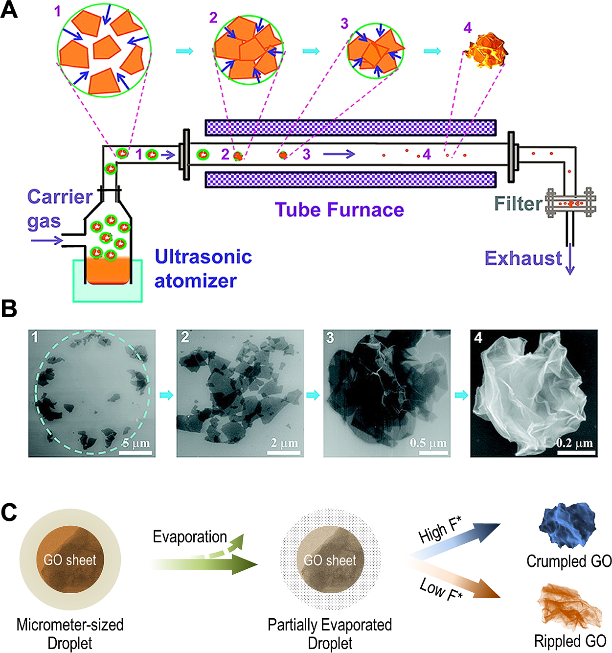
Despite the remarkable properties, graphene or RGO sheets have an intrinsic problem, that is, they have a strong tendency to restack and aggregate due to the van der Waals attraction, which would significantly reduce the surface area and compromise the conductivity (Wang W.N. and He X., 2016). As pointed out by Yang et al. (Yang M.-Q. et al., 2014), because of the aggregation, the so-called semiconductor/graphene composites, under some circumstances, are essentially the same as the other semiconductor-carbon (e.g., fullerenes and carbon nanotubes) counterparts. Preventing the graphene or RGO sheets from aggregation is the key, which, however, is hardly achieved by using conventional methods. On the other hand, the spray process provides a promising strategy to address this issue by creating crumpled graphene balls (Chen Y. et al., 2018; El Rouby W.M.A., 2015; Gao Z. et al., 2018; Luo J. et al., 2011; Ma X. et al., 2012; 2013; Mao B.S. et al., 2014; Mao S. et al., 2012; Wang W.N. et al., 2012; Zangmeister C.D. et al., 2012). During the solvent evaporation process, the 2D GO sheets inside the microdroplets will be crumpled into three dimensional (3D) spheres (i.e., crumpled graphene oxide, CGO) (Figs. 6A and B) by the confinement force resulting from the evaporation (Fig. 6C) (Wang W.N. et al., 2012). The unique crumpled structure enables CGO aggregation-resistant (Luo J. et al., 2011), while still maintains a high surface area (over 1500 m2/g), 58.6 % of the original value (Cranford S.W. and Buehler M.J., 2011; El Rouby W.M.A., 2015), which offers stable anchoring sites for the semiconductor nanocrystals. One additional benefit of the spray process is that, the GO can simultaneously be thermally reduced during the spray process, providing CGO with desirable electrical conductivity.
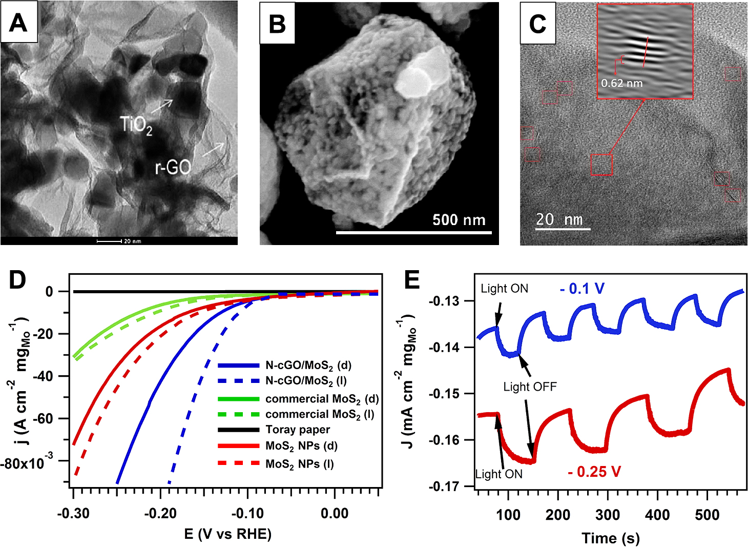
Given all these advantages mentioned above, numerous studies have been carried out to synthesize the CGO/semiconductor composite photocatalysts (Carraro F. et al., 2015; Jiang Y. et al., 2014; Nie Y. et al., 2016; Wang W.N. et al., 2014). For instance, a spray approach was applied by Wang et al. to produce CGO/TiO2 composites (Fig. 7A), where TiO2 nanoparticles were encapsulated in the crumpled structure (Wang W.N. et al., 2014). The as-prepared composite demonstrated improved CO2 photoreduction efficiency, and the mechanism was found to be the facilitated charge carrier separation induced by charge trapping ability of CGO. Besides, the CGO can also be amine functionalized to facilitate adsorption of CO2, which would further enhance the CO2 photoreduction efficiency (Nie Y. et al., 2016). In addition, a CGO/CoO hybrid catalyst (Fig. 7B) was designed with the similar strategy (Mao S. et al., 2014). Furthermore, Carraro et al. used a spray approach to fabricate an N-doped CGO/MoS2 hybrid (Fig. 7C) in a fast and high-yield manner (Carraro F. et al., 2015), where the existence of N-doped CGO significantly enhanced photoelectrochemical production of hydrogen. The improved efficiency is mainly due to the enhanced charge carrier separation, as evidenced by the fact that N-doped CGO/MoS2 hybrid has a much higher current density (Figs. 7D and E) compared with bare MoS2 (Carraro F. et al., 2015). Materials, other than semiconductor photocatalysts, can also be supplemented in the crumpled structure to obtain additional functions. For example, Jiang et al. designed a ternary CGO/TiO2/magnetite nanocomposite (Jiang Y. et al., 2014), which not only exhibited enhanced photocatalytic ability (20 times of the bare TiO2), but also allowed easy recycle and reuse.
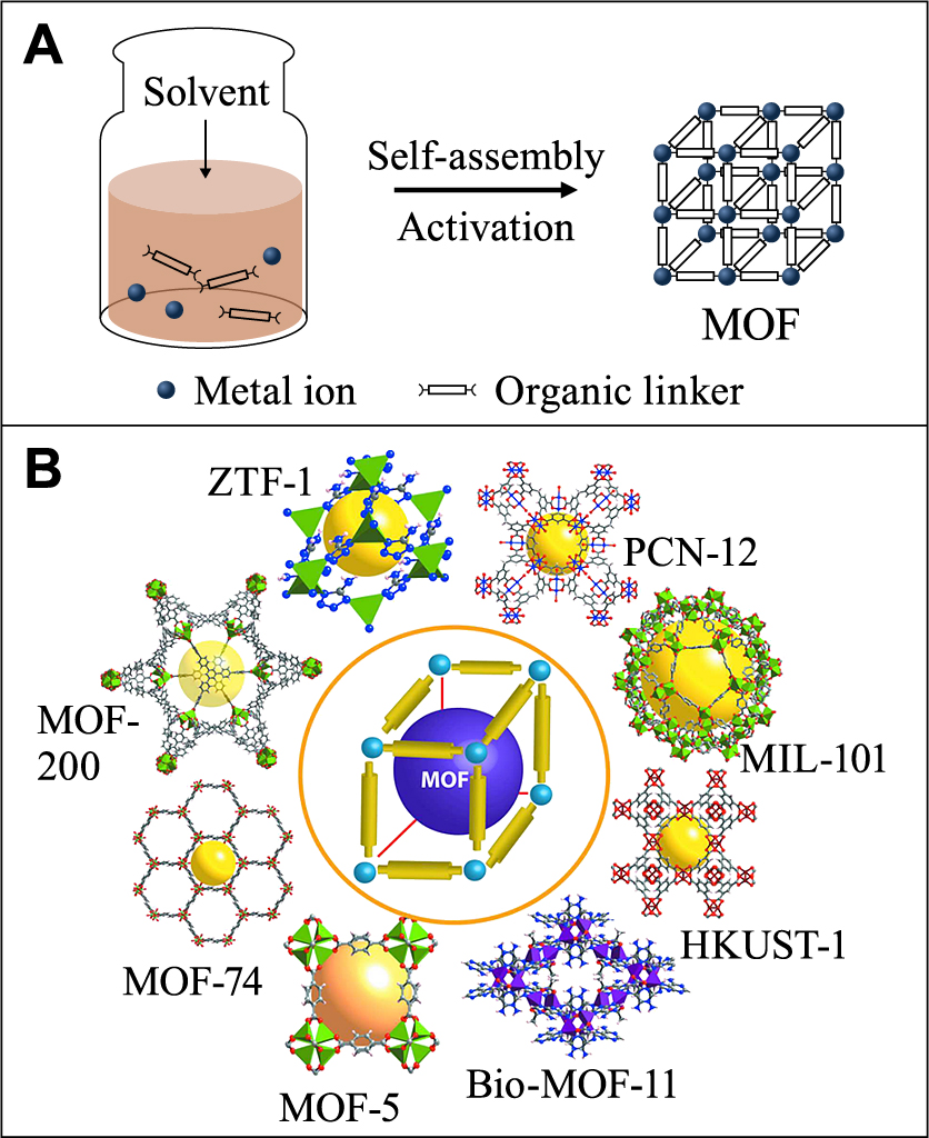
As a new class of porous materials, MOFs have attracted intense attention during recent years. MOFs are composed of metal cations and organic ligands (Fig. 8A (Lee Y.-R. et al., 2013)), and exhibit exceptional properties, including large surface area, high porosity and tunable structure. Schematic illustration of typical MOFs is shown in Fig. 8B (Dey C. et al., 2014), including HKUST-1 (HKUST: Hong Kong University of Science and Technology), MIL-101 (MIL: Material of Institute Lavoisier), and MOF-5. The occurrence of MOFs provides new opportunities to address the long-standing issues in semiconductor-based photocatalysis processes, including but not limited to the deficient gas adsorption, fast recombination of charge carriers, and poor molecule activation. To be specific, when incorporated with semiconductors, MOFs can help increase the adsorption of reactants, and provide more molecules to the surface of semiconductors (He X. et al., 2017a; He X. et al., 2017b). Besides, some MOFs possess coordinatively unsaturated metal sites (or simply called open metal sites), which could act as sinks for charge carriers or electron donors for molecule activation (He X. and Wang W.N., 2018).
Therefore, numerous efforts have been made to design MOF/semiconductor composites, including UiO-66/g-C3N4 (UiO: University of Oslo) (Wang R. et al., 2015), TiO2/ZIF-8 (ZIF: zeolitic imidazolate framework) (Liu Q. et al., 2017; Zeng X. et al., 2016), and TiO2/HKUST-1 (Li R. et al., 2014; Wang H. et al., 2016). For instance, UiO-66/g-C3N4 composite photocatalyst was designed for hydrogen production, and the composite shows significant enhancement in the production rate than that of the counterparts (Wang R. et al., 2015). The enhancement is found to be attributed to the effective separation of photo-induced charge carriers at the interface. Liu et al. integrated ZIF-8 onto the mesoporous TiO2 nanobeads, and achieved promoted performance for Cr(VI) reduction, which was attributed to not only the enhanced adsorption of Cr(VI), but also facilitated interfacial charge transfer (Liu Q. et al., 2017).
It should be noted that, the conventional synthesis of MOFs via wet-chemistry methods usually needs a long reaction duration, where the inefficient heat and mass transfer is inevitable. In this regard, the spray process is a promising alternate route for the rapid synthesis of MOFs (He X. et al., 2017a). As illustrated in Fig. 9, the rapid formation of MOFs within the microdroplets is primarily driven by the enhanced microscopic heat and mass transfer within the microdroplets. The theoretical calculations carried out by our group confirmed that the heat and mass transfer of the precursor within the microdroplets reaches equilibrium within milliseconds, which is much faster than that in bulk synthesis processes and benefits the subsequent nucleation and crystal growth (He X. et al., 2017a). In addition to the synthesis of pristine MOFs, the spray-drying process was applied to tune the properties of these porous materials or design MOF/semiconductor composite (Garcia Marquez A. et al., 2013; Garzón-Tovar L. et al., 2017; He X. et al., 2017a). For example, the spray-drying strategy was applied to produce 14 different discrete nanoMOFs, where the production time and cost were drastically reduced (Carné-Sánchez A. et al., 2013).

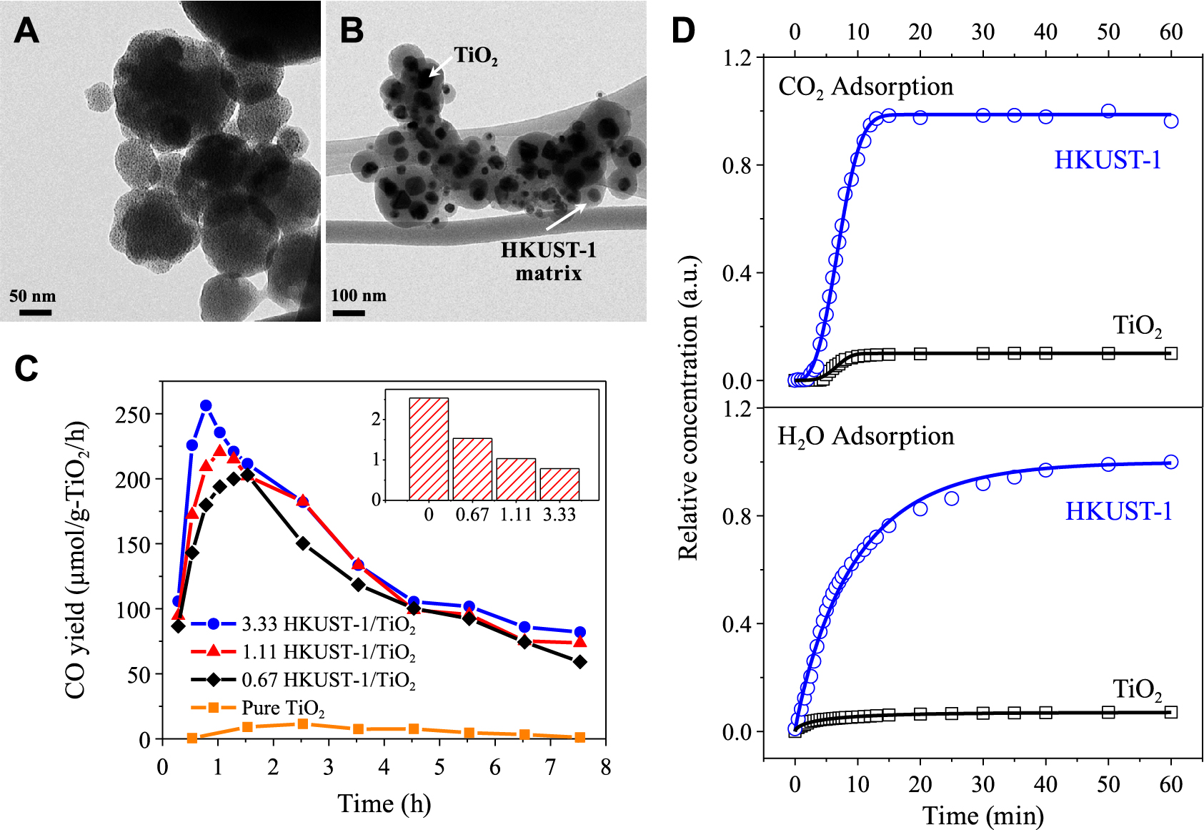
Recently, Cu3(TMA)2 (or HKUST-1, TMA stands for trimesic acid) and TiO2/Cu3(TMA)2 (or TiO2/HKUST-1,) composite photocatalyst were designed by our group through the spray process (Figs. 10A and B) (He X. et al., 2017a). The precursor components were mixed within the microdroplets after the liquid atomization, which ensured the homogeneous distribution of TiO2 in the matrix of HKUST-1 after the synthesis process (Fig. 10B). Besides, the incorporation of TiO2 did not affect the crystallinity of MOF. While, the temperature played an important role in the properties of the as-prepared MOF/semiconductor composite, including crystallinity and surface chemistry. To be specific, the increased temperature (up to 300 °C) decreased the crystal size of the MOF due to the faster nucleation rate over growth rate. At higher temperatures (> 300 °C), the MOF turned amorphous as a result of the disintegration of the organic ligand, which is consistent with the changes in the color of the MOF. The surface chemistry of the MOF synthesized at various temperatures was evaluated by using Fourier transform infrared spectroscopy (FT-IR). At low synthesis temperature, the MOF has similar functional groups as the organic ligand (i.e., TMA). The slight difference in the FT-IR peaks between MOF and the ligand was due to the deprotonation and subsequent coordination of the organic ligand with the metal ions. When the temperature exceeded 300 °C, the adsorption bands weakened or disappeared because of the decomposition of the framework, which was in a good agreement with XRD analysis. The as-prepared HKUST-1/TiO2 composite was applied for CO2 photoreduction. The results revealed that HKUST-1 did not have the photocatalytic ability to reduce CO2 but acted as a major adsorbent to capture CO2 and H2O molecules (Fig. 10D), which subsequently improved the reaction rate and the production yield (Fig. 10C).

;%0A%09%09%09newWindow.document.open();%0A%09%09%09newWindow.document.write('<img src=%22./Graphics/36_2019014_11.jpg%22>');%0A%09%09%09newWindow.document.close();%0A%09%09)
;%0A%09%09%09newWindow.document.open();%0A%09%09%09newWindow.document.write('<img src=%22./Graphics/36_2019014_12.jpg%22>');%0A%09%09%09newWindow.document.close();%0A%09%09)