Abstract
A stable n-type semiconductor material, ZnPcF16, was synthesized and characterized by infrared (IR), UV-vis and fluorescence spectra. ZnPcF16 showed a monomer characteristic in 1, 2-dichlorobenzene (DCB) while exhibited an aggregation property in tetrahydrofuran (THF) and dimethylformamide (DMF). The ZnPcF16/p-6p (ZnPcF16 on p-6p) organic thin film transistors (OTFTs) using ZnPcF16 as an active layer and p-6p as an inducing layer was fabricated by the physical vapor deposition technique. The ZnPcF16 semiconductor film was characterized by XRD and SEM. And the results showed that ZnPcF16 molecules can be oriented after the employment of the p-6p inducing layer. Charge carrier field-effect mobility (µ) and threshold voltage (VT) of the ZnPcF16/p-6p OTFTs were 1.3 × 10⁻² cm2/V s and 22 V, respectively.
1. Introduction
Organic thin film transistors (OTFTs) employing organic semiconductors as the active layer have received widely studies because of their potential application in displays, logic circuits and sensors.1–3) To date, the performance of p-type pentacene-based OTFTs has reached the level of a-Si devices.3,4) Compared with p-type materials, the mobility of the n-type materials with high air stability is relatively low. The search for high performance and stable n-type organic semiconductors has been a challenging task.5)
Phthalocyanines (Pc) show a long standing record of interest in both basic research and applications referring to their photoelectrical properties.6) Copper hexadecafluorophthalocyanine (CuPcF16) is one of the few promising n-type candidates as air stable and high mobility semiconductor materials.7) Synthesis and investigations of CuPcF16 were described in reference literature.8) To improve the performance of CuPcF16-based OTFTs, Yan et al.3) employed an organic heterojunction buffer layer to decrease the contact resistance of organic/metal. The electron field-effect mobility is exponentially enhanced from 4.2 × 10⁻² to 7.6 × 10⁻² cm2/V·s. Fan et al.9) have reported CuPcF16-based transparent OTFTs based on Ag/LiF bilayer transparent S/D electrodes with good electron mobility of 1.31 × 10⁻² cm2/V·s. The fluorination of p-type metal phthalocyanines may produce n-type semiconductors, allowing many n-type semiconductors designed in accordance with this approach.5,9)
Although the synthesis of fluorinated metal phthalocyanines has been reported,8,10,11) the fundamental properties of hexadecafluorinated phthalocyanines have not been sufficiently studied.8) In this paper, zinc hexadecafluorophthalocyanine (ZnPcF16, shown in Fig. 1) was synthesized in a slightly modified procedure and its spectral properties were characterized. Especially we employed p-6p (shown in Fig. 1) as an inducing layer to fabricate ZnPcF16-based thin film transistors using the vapor deposition techniques and investigated their electrical characteristics.
2. Experimental Procedures
For the synthesis of ZnPcF16, sublimed tetrafluorophthalonitrie and zinc acetate in an equimolar 4:1 ratio were intensively mixed in a mortar. The mixture was filled in a glass vessel, three times flushed with nitrogen and vacuum and finally the glass ampoule was sealed under vacuum (1.33 × 10⁻³ Pa). After heating for 8 h at 220℃ the blue product was isolated and washed with ethanol and acetone to remove the soluble organic admixture. The resulting blue deposit with yield of 48.2% after purification by concentrated sulfuric acid was identified as zinc hexadecafluorophthalocyanine. IR (KBr) 1610, 1523, 1450, 1148, 832 and 745 cm−1. MS (TOF, Methanol) m/e 865.76. The ZnPcF16/p-6p OTFTs configuration is given in Fig. 2. The device was prepared with a semiconductor ZnPcF16 and a rod-like conjugated oligomer p-6p molecule. ZnPcF16 and p-6p were purified twice by thermal gradient sublimation prior to processing. A 6 nm thick film of p-6p was first deposited on a SiO2 substrate at 180℃, and then a 30 nm thick layer of ZnPcF16 was deposited on top of the p-6p surface by vacuum deposition.

All organic films were deposited by vapor deposition in vacuum (10−4–10−5 Pa) at a rate of 0.50 nm min−1. Finally, Au source and drain electrodes with 30 nm thickness were prepared by thermal deposition with a shadow mask defining channel width (W) and length (L) of 6000 µm and 200 µm, respectively. The output and transfer characteristics of the transistors were measured with two Keithley 2400 source-measurement units under ambient conditions at room temperature.
3. Results and Discussion
3.1 UV-vis and fluorescence spectra
Figure 3 shows the UV-vis absorption spectra of 5 × 10⁻⁵ mol L−1 ZnPcF16 solutions in 1, 2-dichlorobenzene (DCB), tetrahydrofuran (THF) and dimethylformamide (DMF), respectively. The absorption spectra were measured by an EVOLUTION300 spectrometer. Absorption maxima for Q band are seen at 680 nm with shoulder peak at 650 nm for ZnPcF16 dissolved in DCB and at 644 and 640 nm for ZnPcF16 solution in THF and DMF. The absence of aggregation effects indicates monomer behavior of ZnPcF16 in DCB.8,11) And with the increase of the polarity of solvents, the ground state is more stable than the excited state in the π-π* transition system, so the transition energy gap increases, which will induce the Q band shift to a shorter wave length to some extent. The spectrum of ZnPcF16 dissolved in THF differs from the spectrums of this compound in DCB solvents since it shows two strong absorption peaks at 644 and 674 nm. It demonstrates that ZnPcF16 aggregates in THF solvent according to reference literature.8,11)

Figure 4 shows the UV-vis absorption curves of different concentrations of ZnPcF16 in DMF. In the low concentration region, there are two strong absorption peaks at 640 and 674 nm for Q band. With the concentration of ZnPcF16 increasing, the absorption peak at about 640 nm grows while the intensity of absorption peak at 674 nm declines and even disappears. It is a typical UV-vis absorption pattern for aggregation behavior. The higher the concentration, the more easily it aggregates in DMF.
The fluorescence spectrum of ZnPcF16 in DCB was measured on a CARY Eclipse fluorescence spectrophotometer, as shown in Fig. 5. The emission maxima are observed at 728 nm corresponding to the red light emission.
3.2 Thermal properties
The thermal properties of ZnPcF16 were characterized by thermogravimetric analysis (TGA) at a heating rate of 10℃ min−1 under nitrogen atmosphere. The TGA curve was measured by a TG 209 F3 thermo gravimetric analyzer. ZnPcF16 is relative stable and the mass loss is less than 10% below 100℃. TGA measurements indicate that ZnPcF16 compound has high decomposition temperature of 497℃ (Td, correspond to a 10% mass loss, Fig. 6). ZnPcF16 exhibits excellent thermal stability and so its semiconductor thin film can be prepared by thermal deposition technique.
3.3 XRD of ZnPcF16/p-6p film
Figure 7 shows the XRD pattern of the ZnPcF16/p-6p thin film. The X-ray diffraction was performed in a Rigaku D/max 2500 PC X-ray diffractometer with a Cu Kα radiation (λ = 1.54056 Å). The diffraction peaks of the ZnPcF16/p-6p film at diffraction angle 2θ = 6.24, corresponding to d200 spacing of 14.15 Å, are observed. According to the reference literatures and the process for preparing semiconductor thin films by vapor deposition, the XRD pattern indicates that the ZnPcF16 molecules are approximately standing-up on the p-6p layer.12–15)
3.4 SEM of ZnPcF16/p-6p film
The SEM image was obtained by a FEI Nanosem 430 electron microscopy instrument. The surface image of ZnPcF16/p-6p thin film is shown in Fig. 8. Dish-like ZnPcF16 molecules can be oriented to form high quality semiconductor thin films. The image shows a strip grain pattern of ZnPcF16/p-6p film. It implies that the π-π stack direction of the ZnPcF16 molecules is parallel to the p-6p layer, which will facilitate the carrier transportation.
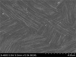
The growth behavior of the p-6p thin film has been studied systematically.16,17) A highly-ordered smooth p-6p ultrathin film can supply a high quality substrate for the growth of phthalocyanine molecules. The phthalocyanine molecules can be oriented on the inducing layer of rod-like p-6p molecules, which likely results from the geometrical channels of the p-6p layer surface and the dominant direction of semiconductor molecules on the p-6p thin film surface. And through the method of organic vapor deposition at high substrate temperature, organic phthalocyanine molecules can grow upright on the substrate. Thus the π-π conjugated direction is parallel to the p-6p layer.
3.5 Current-voltage characteristics
Typical output characteristic curves of the ZnPcF16/p-6p OTFTs are shown in Fig. 9 at different gate-source voltages (VGS) from 0 to 100 V. The positive voltage signals imply an electron-accumulated process in these OTFTs. With the increase of VDS, the linear region and the saturation region can be observed. At VGS = 0 V, IDS tends to 0 A for VDS < 60 V and IDS is increased sharply with the increasing VDS for the VDS > 60 V. At VGS = 20 and 40 V, IDS only shows weak current value for VDS from 0 to 100 V. At VGS = 60, 80 and 100 V, IDS is almost linearly increased with increasing VDS for lower VDS from 0 to 30 V while IDS tends to saturate for higher VDS above 30 V.

In the electron accumulating mode, when the drain voltage is low, the saturated region continues to be compressed as VGS decreases, but for a high drain voltage, IDS increases dramatically as VDS increases. This is a typical ambipolar transport character, and both electrons and holes can be transported in the semiconductor. The p-6p is a p-type semiconductor, while ZnPcF16 is an n-type semiconductor. Due to the heterojunction effect, the transistor presents ambipolar behavior.
Figure 10 shows the typical transfer characteristics of the ZnPcF16/p-6p OTFTs with different gate voltages at a fixed VDS of 100 V. The field effect mobility was extracted from Fig. 10 in the saturation region (V ≥ (VGS − VT)) based on
| \[
I_{\rm DS} = \frac{W}{2L} \mu C_{\rm i} (V_{\rm GS} -
V_{\rm T})^2\] | (1) |
Where
IDS is the drain-source current,
W and
L are the width and length of the channel, respectively,
µ is the field-effect mobility,
VGS is the gate voltage and
VT is the threshold Voltage. The capacitance per unit area of the insulator (
Ci) is 8 nF/cm
2. When a positive
IDS is observed upon the application of positive
VGS and
VDS, the semiconductor is
n-type since the electrons are mobile. According to the electrical properties,
n-type conductivity of the ZnPcF
16 semiconductor material was confirmed. The field effect mobility of 1.3 × 10
−2 cm
2/V s and the threshold Voltage of 22 V were extracted from the saturation region in
Fig. 10.
4. Conclusions
In summary, an n-type semiconductor material, ZnPcF16, was synthesized and characterized by infrared (IR), MS, UV-vis and fluorescence spectra. The ZnPcF16-based OTFTs using p-6p as the inducing layer was fabricated by the physical vapor deposition technique. The electrical properties of the OTFTs were investigated and n-type of conductivity was confirmed. And the charge carrier field-effect mobility of the ZnPcF16/p-6p OTFTs was 1.3 × 10⁻² cm2/V s. The stable ZnPcF16 compound with high mobility will be a promising material for optical and electronic devices application.
Acknowledgements
The authors are grateful to Donghang Yan research group in Changchun Institute of Applied Chemistry of Chinese Academy of Sciences for support of devices' fabrication. The work has been partially supported by National Natural Science Foundation of China (no. 21401138), High School Science and Technology Fund Planning Project of Tianjin (no. 20130508).
REFERENCES
- 1) H.E.A. Huitema, G.H. Gelinck, J.B.P.H. Van Der Putten, K.E. Kuijk, C.M. Hart, E. Cantatore and D.M. De Leeuw: Adv. Mater. 14 (2002) 1201–1204. 10.1002/1521-4095(20020903)14:17<1201::AID-ADMA1201>3.0.CO;2-5
- 2) B. Crone, A. Dodabalapur, Y.Y. Lin, R.W. Filas, Z. Bao, A. Laduca, R. Sarpeshkar, N.E. Katz and W. Li: Nature 403 (2000) 521–523. 10.1038/35000530
- 3) X. Yan, J. Wang, H. Wang, H. Wang and D. Yan: Appl. Phys. Lett. 89 (2006) 053510.
- 4) T.N. Jackson, Y.Y. Lin, D.J. Gundlach and H. Klauk: IEEE J. Sel. Topics Quantum Electron. 4 (1998) 100–104. 10.1109/2944.669475
- 5) A. Facchetti: Mater. Today 10 (2007) 28–37. 10.1016/S1369-7021(07)70017-2
- 6) T. Oku, N. Kakuta, A. Kawashima, K. Nomura, R. Motoyoshi, A. Suzuki, K. Kikuchi and G. Kinoshita: Mater. Trans. 49 (2008) 2457–2460. 10.2320/matertrans.MB200807
- 7) T. Wang, D. Ebeling, J. Yang, C. Du, L. Chi, H. Fuchs and D. Yan: J. Phys. Chem. B 113 (2009) 2333–2337. 10.1021/jp8080639
- 8) E. Kol'tsov, T. Basova, P. Semyannikov and I. Igumenov: Mater. Chem. Phys. 86 (2004) 222–227. 10.1016/j.matchemphys.2004.03.007
- 9) N. Zhang, J. Lin, J. Luo, Y. Li, Z. Gan, Y. Fan and X. Liu: Appl. Phys. Express 7 (2014) 021601. 10.7567/APEX.7.021601
- 10) S. Hiller, D. Schlettwein, N.R. Armstrong and D. Wöhrle: J. Mater. Chem. 8 (1998) 945–954. 10.1039/a707485i
- 11) M. Handa, A. Suzuki, S. Shoji, K. Kasuga and K. Sogabe: Inorg. Chim. Acta 230 (1995) 41–44. 10.1016/0020-1693(94)04188-2
- 12) H. Wang, F. Zhu, J. Yang, Y. Geng and D. Yan: Adv. Mater. 19 (2007) 2168–2171. 10.1002/adma.200602566
- 13) Z. Bao, A.J. Lovinger and A. Dodabalapur: Adv. Mater. 9 (1997) 42–44. 10.1002/adma.19970090108
- 14) Z. Bao, A.J. Lovinger and J. Brown: J. Am. Chem. Soc. 120 (1998) 207–208. 10.1021/ja9727629
- 15) J. Yang and D. Yan: Chem. Soc. Rev. 38 (2009) 2634–2645. 10.1039/b815723p
- 16) J. Yang, T. Wang, H. Wang, F. Zhu, G. Li and D. Yan: J. Phys. Chem. B 112 (2008) 7816–7820. 10.1021/jp711455u
- 17) J. Yang, T. Wang, H. Wang, F. Zhu, G. Li and D. Yan: J. Phys. Chem. B 112 (2008) 7821–7825. 10.1021/jp711457p


