Abstract
Ta-inserted SmCo5/Fe nanocomposite thick film magnets were synthesized by high-speed pulsed laser deposition followed by pulse annealing. The microstructures of the film magnets were characterized by high-resolution scanning electron microscopy and scanning transmission electron microscopy. The as-deposited thick film possessed a multilayered Sm-Co/Ta/α-Fe/Ta structure with amorphous Sm-Co layers and [110]-oriented crystalline α-Fe layers. After pulse annealing, many fine grains of Laves phase TaCo2 were formed, and then the multilayered structure was converted to a granular nanocomposite thick film magnet composed of fine crystalline grains of Sm(Co, Fe)5, α-(Fe, Co), and TaCo2. The volume fractions and grain sizes of hard magnetic Sm(Co, Fe)5, soft magnetic α-(Fe, Co), and TaCo2 were controlled by the thicknesses of the Ta layer, producing a nanocomposite thick film magnet with good exchange coupling.
1. Introduction
Permanent magnets that can be used at high temperatures (>200 ℃) and that do not contain heavy rare-earth elements are required. SmCo5/α-Fe nanocomposite magnets have attracted much attention because of the high Curie temperature of SmCo5 (Tc~747 ℃) and the large saturation magnetization of α-Fe (Ms~2.16 T). Neu et al.1,2) achieved epitaxial growth of [SmCo5/α-Fe]n/SmCo5 (n = 1 − 5) multilayers by pulsed laser deposition (PLD) and an energy density of more than 400 kJ/m3 was realized in the thin film of n = 2 (total thickness of about 75 nm). Sub-millimeter thick film magnets are required for practical applications. Fukunaga et al.3,4) reported that Sm-Co/α-Fe multilayered thick film magnets were fabricated by high-speed PLD.5,6) However, the interlayer diffusion of Fe and Co was increased by crystallization during annealing, degrading the magnetic properties.
In this study, we synthesized SmCo5/Ta/α-Fe/Ta multilayered thick film magnets, in which a Ta layer was inserted between the Sm-Co and α-Fe layers. We chose Ta as the diffusion barrier layer because Ta is a refractory metal and is expected to work as a diffusion barrier. The microstructures of the synthesized film magnets were investigated by high-resolution scanning electron microscopy (HRSEM) and scanning transmission electron microscopy (STEM). Based on these results, we discuss the synthetic conditions for obtaining higher performance SmCo5/α-Fe thick film magnets.
2. Experimental
A diagram of the high-speed PLD method using a composite target is shown in Fig. 1. Two kinds of composite targets, which were composed of SmCo5, α-Fe, and Ta segments, were prepared with different area fractions. The targets were ablated with a Nd:YAG laser and rotated at a speed of 6.5 rpm during the ablation, and then two kinds of multilayered films were deposited on Ta-foil substrates at room temperature. For both films, the distance between the target and the substrate was 10 mm and the deposition time was 3.6 ks. The nominal structures of one cycles for these two films were [Sm-Co (18 nm)/Ta (1.3 nm)/Fe (5 nm)/Ta (1.3 nm)] (STF-1) and [Sm-Co (11 nm)/Ta (0.5 nm)/Fe (4 nm)/Ta (0.5 nm)] (STF-2). The Sm-Co layers in the as-deposited STF-1 and STF-2 films were amorphous, and they were crystallized by pulse annealing for about 2.0 s in an infrared furnace with an output power of 8 kW under a high vacuum of 5 × 10⁻⁴ Pa.5–7) Although we could not measure the sample temperature Ts because of its extremely high ramp rate, the peak value of Ts is estimated to be higher than 873 K, because magnetic hardening for our specimens occurs by an isothermal annealing higher than 873 K.

The in-plane magnetic properties of the films were evaluated with a vibrating sample magnetometer (TM-VSM2430, Tamagawa) after magnetization under a pulsed magnetic field of 6.4 MA/m. Microstructure analyses were performed by HRSEM (Ultra 55, Carl Zeiss) and STEM (Titan Cubed, FEI). The specimens for HRSEM and STEM were fabricated by Ga focused ion beam (FIB) milling (Versa 3D DualBeam, FEI) with a lift-off technique. Surface damage caused by FIB milling was removed by low-angle Ar ion milling (1050, Fischione Instruments). The STEM observations and energy dispersive X-ray spectroscopy (EDS) analysis were carried out by STEM with an EDS system containing four windowless Si drift detectors (Titan Cubed, Super-X, FEI).
3. Results and Discussion
Figures 2(a) and (b) show the hysteresis loops of the pulse-annealed STF-1 and STF-2 specimens. The hysteresis measurements were carried out with the applied field parallel to the film plane. The observed hysteresis curves are asymmetric with respect to the applied magnetic field, which suggests that magnetization of Sm-Co is not reversed in places under the maximum negative applied field (approximately 1.9 MA/m) because of their high coercivity. Both of the hysteresis loops exhibit smooth curves without steps, indicating single-phase-like behavior with strong exchange coupling between the soft and the hard magnetic phases. The STF-1 specimen has a high coercivity (Hc = 958 kA/m), although the remanence is low (Fig. 2(a)). In contrast, the STF-2 specimen has a high remanence (Br = 0.67 T) and energy density ((BH)max = 59 kJ/m3) (Fig. 2(b)).

Figures 3(a) and (b) show the HRSEM back-scattered electron (BSE) images of the as-deposited and the pulse-annealed STF-1 specimens, where the BSE images mainly reflect the Z-contrast, or the compositional contrast.8) In the as-deposited specimen (Fig. 3(a)), thin layers with bright and dark contrasts are alternately deposited on the micrometer scale, although several droplets are formed. The enlarged image (inset of Fig. 3(a)) clearly indicates that a multilayered structure is formed by depositing thin films with a period of about 20 nm per cycle. In the pulse-annealed specimen (Fig. 3(b)), the multilayered structure almost disappears and a nanocomposite texture consisting of fine particles is formed. These results indicate that the multilayered structure is converted to a granular nanocomposite texture by pulse annealing.

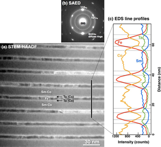
Figures 4(a) and (b) show the STEM high-angle annular dark field (HAADF) image and the selected area electron diffraction (SAED) pattern of a typical microstructure for the as-deposited STF-1 specimen. In Fig. 4(a), the image contrast roughly reflects the Z-contrast (the averaged atomic numbers), showing that the Ta thin layers (brightest layers) are formed on both sides of the Fe layers (darkest layers). The multilayered structure consists of [Sm-Co (14 nm)/Ta (3 nm)/α-Fe (5 nm)/Ta (3 nm)], and the thickness of one cycle is approximately 25 nm. This layer is thinner than the thin film fabricated by Neu et al.,1) and is the same as that in the ideal nanocomposite magnet predicted by Fukunaga et al.9) The main diffraction spots in Fig. 4(b) correspond to the reflections of α-Fe $[ \bar 111]$ incidence, indicating that the α-Fe layers in the multilayered structure are formed with [110] oriented along the deposition direction. The SmCo5 layers are amorphous because the diffuse rings appear around the positions that correspond to the lattice spacing of SmCo5 (P6/mmm, hexagonal, CaCu5 structure10)). Figure 4(c) shows the STEM-EDS line profiles of Sm, Co, Fe, and Ta obtained from the position indicated by the black line in Fig. 4(a). The intensity of Co is high in the SmCo5 layers and in the Ta layers. In addition, some Co penetrates into the Fe layers, and a solid solution of α-(Fe, Co) is formed. The Ta layers between the SmCo5 and α-Fe layers also contain a large amount of Co, because the line profile of Co shows the peaks at the Ta layers. Because the atoms ablated during PLD had high kinetic energy, we consider that the Sm(Co, Fe)5, α-(Fe, Co), and Ta-Co layers were formed by mutual diffusion after the atoms reached the substrate.
The STEM-HAADF image and the SAED pattern of the typical microstructure of the pulse-annealed STF-1 specimen are shown in Figs. 5(a) and (b). In the enlarged image (inset of Fig. 5(a)), there are three types of fine grains: α-(Fe, Co) grains of about 40 nm in diameter, visible as dark contrast; Sm(Co, Fe)5 grains of about 60 nm in diameter, visible as gray contrast; and Ta-Co grains of about 30 nm in diameter, visible as bright contrast. The SAED pattern of Fig. 5(b) indicates that the amorphous Sm(Co, Fe)5 layers are crystallized to form many fine Sm(Co, Fe)5 grains with random orientations. Furthermore, the [110]-oriented α-(Fe, Co) layers are transformed to fine crystalline grains with random orientations. High-resolution TEM (HRTEM) was performed to explain the destruction of the multilayered structure.

Figure 6 shows the HRTEM image of part of the typical texture of the pulse-annealed STF-1 specimen, where a pentagonal grain with many planar defects is observed in the central part of the image. Figures 6(c)–(e) show Fourier spectra obtained from areas 1–3 in Fig. 6(a). The Fourier spectra indicate that the α-Fe and SmCo5 phases are formed in areas 1 and 3, respectively. In FFT-2, diffraction spots corresponding to a MgCu2(C15) Laves phase structure appear with streaks along the [111] direction, indicating that the pentagonal grain in Fig. 6(a) is an intermetallic TaCo2 compound. MgCu2 Laves phases are frequently formed in the AB2 (A = Zr, Nb, Hf, Ta; B = Mn, Fe, Co, Ni) alloys and often contain a large amount of {111} planar defects.11,12) Furthermore, MgCu2 Laves phases show interesting magnetic properties, such as metamagnetic transitions; however, TaCo2 is a paramagnetic phase, except for at low temperatures.13) Thus, during pulse annealing, Ta and Co react easily to form many fine crystalline TaCo2 grains. Consequently, the multilayered structure is converted to a granular nanocomposite texture that consists of grains of hard magnetic Sm(Co, Fe)5, soft magnetic α-(Fe, Co), and paramagnetic TaCo2.
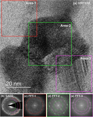
Figure 7 shows the STEM-HAADF image and EDS chemical maps for the pulse-annealed STF-1 specimen. In the overlaid map (Fig. 7(f)), the blue, pink, and yellow-green areas correspond to fine grains of Sm(Co, Fe)5, α-(Fe, Co), and TaCo2, respectively. The sizes and distributions of the fine grains of the three phases are visualized in the overlaid map. Similar STEM analysis was performed for the STF-2 specimen. The STEM-EDS overlaid maps of the typical microstructures for the pulse-annealed STF-1 and STF-2 specimens are shown in Figs. 8(a) and (b), respectively. There are fewer TaCo2 grains in STF-2 than in STF-1, and the grains are larger. The Sm(Co, Fe)5 and α-(Fe, Co) grains grow bigger in STF-2. The volume fractions, V, and the average grain sizes, Da, estimated from the EDS maps are listed in Table 1. The volume fraction of TaCo2 in STF-1 (~24%) is higher than that in STF-2 (~18%). This means that the thicker Ta layer in the as-deposited state produces a larger amount of TaCo2 after annealing. However, there are fewer, smaller α-(Fe, Co) grains in STF-1 than in STF-2, regardless of the layer thickness. This suggests that the diffusion of Co from Sm(Co, Fe)5 to α-(Fe, Co) is suppressed as the Ta interlayer thickness increases. Furthermore, in STF-1 with thick Ta layers, grain growth beyond each layer is suppressed, and the Sm(Co, Fe)5 and α-(Fe, Co) grain sizes remain small. Therefore, in the STF-1 specimen, the thick Ta layer produces a large amount of hard magnetic Sm(Co, Fe)5, and the small grain sizes of the hard and soft magnetic phases produce the high coercivity (Hc = 958 kA/m). In the STF-2 specimen, the thin Ta layer produces a large amount of soft magnetic α-(Fe, Co) and relative large grain sizes in all phases, leading to the high remanence (Br = 0.67 T) and energy density ((BH)max = 59 kJ/m3). Therefore, the volume fractions and the grain sizes were controlled by the thickness of the Ta interlayer.

Table 1
Volume fractions (
V) and average grain sizes (
Da) of Sm(Co, Fe)
5, α-(Fe, Co), and TaCo
2 phases for post-annealed STF-1 and STF-2 specimens.
| Phases |
STF-1 |
STF-2 |
| V (%) |
Da (nm) |
V (%) |
Da (nm) |
| Sm(Co, Fe)5 |
43 |
42 |
30 |
68 |
| α-(Fe, Co) |
33 |
53 |
52 |
107 |
| TaCo2 |
24 |
22 |
18 |
32 |
If the Ta layer is thin, Co diffusion is not suppressed, and the SmCo5 (CaCu5) ordered phase is not formed. However, the TEM results only showed the Sm(Co, Fe)5 phase. Therefore, we assume that the mutual diffusion of Co and Fe between Sm(Co, Fe)5 and α-(Fe, Co) is well balanced. Further investigation of the relationship between the thickness of the Ta interlayer and the composition shifts caused by the mutual diffusion of Co and Fe is required.
Based on our results, higher performance SmCo5/α-Fe nanocomposite thick film magnets should be obtained if the volume fraction of α-Fe can be increased while retaining the thick Ta layer. However, in this type of nanocomposite film magnet, it is difficult to achieve superior magnetic properties equal to those of the Nd-Fe-B magnets, even at the high temperatures (~200 ℃). Consequently, it is necessary to maintain the multilayered structure consisting of fully aligned SmCo5/α-Fe layers by blocking interlayer diffusion. We are currently investigating new interlayer materials.
4. Conclusions
Ta-inserted SmCo5/α-Fe thick film magnets were prepared by high-speed PLD, and the microstructures of the film magnets were characterized by HRSEM and STEM. The following results were obtained.
(1) In the as-deposited films, multilayered thick films can be synthesized on the micrometer scale, where the layer thickness of one cycle, [Sm(Co, Fe)/Ta-Co/α-(Fe, Co)/Ta-Co], is approximately 25 nm with [110]-oriented α-(Fe, Co) layers.
(2) During pulse annealing, fine crystalline grains of Laves phase TaCo2 are formed, and then the multilayered structure is converted to Sm(Co, Fe)5/α-(Fe, Co)/TaCo2 nanocomposite thick film magnets.
(3) The volume fractions and the grain sizes of hard magnetic Sm(Co, Fe)5, soft magnetic α-(Fe, Co), and paramagnetic TaCo2 can be controlled by the thickness of the Ta layers, allowing nanocomposite thick film magnets with specific coercivitiy and remanence to be obtained.
Acknowledgements
This work was partly supported by the New Energy and Industrial Technology Development Organization (NEDO), Japan, and was performed as an extension of a collaborative research supported by the Nanotechnology Platform Project from the Ministry of Education, Culture, Sports, Science and Technology, Japan.
REFERENCES
- 1) V. Neu, S. Sawatzki, M. Kopte, C. Mickel and L. Schultz: IEEE Trans. Magn. 48 (2012) 3599–3602. 10.1109/TMAG.2012.2195646
- 2) S. Sawatzi, R. Heller, C. Mickel, M. Seifert, L. Schultz and V. Neu: J. Appl. Phys. 109 (2011) 123922.
- 3) A. Tou, T. Morimura, M. Nakano, T. Yanai and H. Fukunaga: J. Appl. Phys. 115 (2014) 209901. 10.1063/1.4871335
- 4) H. Fukunaga, A. Tou, M. Itakura, M. Nakano, and T. Yanai: IEEE Trans. Magn. 50 (2014) 2101504. 10.1109/TMAG.2013.2276429
- 5) M. Nakano, S. Sato, F. Yamashita, T. Honda, J. Yamasaki, K. Ishiyama, M. Itakura, J. Fidler, T. Yanai and H. Fukunaga: IEEE Trans. Magn. 43 (2007) 2672–2676. 10.1109/TMAG.2007.893778
- 6) H. Fukunaga, H. Nakayama, T. Kamikawatoko, T. Yanai, M. Nakano, F. Yamashita, S. Ohta, M. Itakura and M. Nishida: J. Phys. Conf. Ser. 266 (2011) 012027.
- 7) M. Nakano, H. Takeda, F. Yamashita, T. Yanai and H. Fukunaga: IEEE Trans. Magn. 44 (2008) 4199–4201. 10.1109/TMAG.2008.2001492
- 8) M. Itakura, N. Kuwano, K. Sato and S. Tachibana: J. Electron Microsc. 59 (2010) S165–S173. 10.1093/jmicro/dfq044
- 9) H. Fukunaga and H. Mukaino: J. Rare Earths 22 (2004) 146–151.
- 10) T. G. A. Verhagen: Magnetism and magnetization dynamics in thin film ferromagnets, (Casinir PhD series, Leiden-Delft, 2014), pp. 43–73.
- 11) K.S. Kumar, L. Pang, C.T. Liu, J. Horton and E.A. Kenik: Acta Mater. 48 (2000) 911–923. 10.1016/S1359-6454(99)00377-8
- 12) Y. Liu, J.D. Livingston and S.M. Allen: Metal. Trans. A 23 (1992) 3303–3308.
- 13) H. Yamada, J. Inoue and M. Shimizu: J. Magn. Magn. Mater. 54–57 (1986) 961–962. 10.1016/0304-8853(86)90334-3
