1. Introduction
Due to the increasing environmental concerns, the use of Sn-Pb solder has been banned in electronic products since 2006 by international legislations, which has led to the extensive studies on Pb-free solder materials1), including Sn-Ag-Cu, Sn-Cu, Sn-Ag, Sn-Bi and Sn-Zn2–7), etc. Among these potential alternatives, Sn-58Bi eutectic solder is recently getting much attention due to its lower melting temperature at 139℃, which can obviously reduce the thermal warpage on the components and boards during assembling. Sn-Bi solder joints also have excellent joint strength, low coefficient of thermal expansion, good wettability, superior creep resistance, and improved yield and fracture strength2,8).
With the scaling down of dimensions on packaging components, the current density through the solder bumps will be expected to reach about 104 A/cm2. Under such a current density, the metallic atoms are migrated with the current flow. In Sn-Bi/Cu solder joint, phase separation in the solder and Bi segregation to the interface were always produced at the anode after electromigration9–11). The interfacial embrittlement induced by Bi segregation will deteriorate the reliability of solder joint12). Therefore, to improve the electromigration reliability of Sn-58Bi solder joint, it is necessary to decrease the growth on Bi-rich layer at the anode. Many researchers have added the alloying elements into Sn-58Bi solder and found that the electromigration performances of Sn-58Bi solder were improved. For example, Li et al.13) found that adding tungsten nanoparticles into Sn-58Bi solder improved the electromigration resistance and joint strength. Hu et al.14) proposed the addition of Al2O3 nanoparticles into Sn-58Bi solder reduced the mean thickness of Bi-rich layer at the anode. The addition of Ag nanoparticles was also verified to decrease the formation of Bi-rich layer at the interface and increase the shear strength of Sn-58Bi solder joint after electromigration15). Additionally, with Sn-Ag-Cu solder as the diffusion barrier, the formation of Bi-rich layer at the anode in Sn-58Bi solder joint was also effectively depressed16).
Besides adding alloying elements into Sn-58Bi solder, alloying Cu substrate provides another opportunity to improve the interfacial structure and joint strength of Sn-58Bi solder, which was rarely reported in the literatures. Zou et al.17) and our previous paper18) studied the interfacial structure and joint strength of Sn-58Bi solder on Cu-Zn, Cu-Al and Cu-Ag substrates during isothermal aging, and interestingly found that the intermetallic compounds (IMCs) growth and joint strength were obviously improved by these alloying substrates. Therefore, we further studied the effect of Zn containing Cu substrate on the electromigration behavior of Sn-58Bi solder joint in this paper. The interfacial Bi segregation and the growth of hillocks in Sn-58Bi solder joints on Cu-Zn metallization substrate were investigated and compared with Sn-58Bi solder joints on Cu substrate during electromigration.
3. Results and discussion
Figure 3 shows the backscattered electron (BSE) images on the interfacial microstructure formed between Sn-58Bi solder and Cu or Cu-4.89Zn substrate after soldering at 175℃ for 30 s. A thin IMC layer was observed at both Sn-58Bi/Cu and Sn-58Bi/Cu-4.89Zn interfaces. The composition of IMC was Cu6Sn5 phase confirmed by EDX. It seems minor Zn in Cu substrate did not enroll in the reaction of Cu and Sn. However, Kim et al.20) and Yu et al.21) have proposed that Zn atoms could dissolve into Cu6Sn5 IMC phases by replacing some Sn atoms during the formation of Cu6Sn5 IMC layer. From the microstructural observation, alloying Zn into Cu substrate was slightly beneficial to the refinement of grain size in the Sn-58Bi solder matrix.

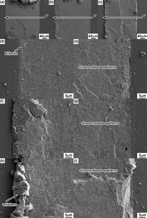
The surface morphology of Cu/Sn-58Bi/Cu solder joints under current density of 1.0 × 10⁴ A/cm2 was examined at intervals to trace the evolution of damage, and the results are shown in Fig. 4. It includes the effect of different stressing time on the cross-sectional joint, the anode interface and the cathode interface, respectively. The direction of electron flow is from the right to the left. Compared with Fig. 2, the surface morphology became rough after current stressing. After 33 h current stressing, the anode side shows a bulging morphology, as shown in Fig. 4(d), while the cathode side shows a dimpling morphology, as shown in Fig. 4(e). In the solder matrix, stress release patterns were observed along the grain boundaries close to the cathode side. After current stressing for 66 h, the step-shaped stress release patterns fully covered the joint, and more hillocks were squeezed out at the anode side, as shown in Fig. 4(f). With stressing time continued to 132 h, continuous extrusion of the hillocks at the anode side promoted the formation of whiskers shown in Fig. 4(h). The rack of lines can be clearly observed at surface of the whiskers, which is usually believed to be the common feature of the whiskers. At the cathode side in Fig. 4(i), continuous current stressing finally promoted the formation of voids. In the cross-sectional solder joint shown in Fig. 4(c), the left area near the anode was higher than the right area near the cathode due to the compressive stress in the anode region and the tensile stress in the cathode region, which will be discussed later.

With 4.89 mass% Zn alloyed into Cu substrate, Fig. 5 shows the corresponding surface morphologies after current stressing. After current stressing for 33 h, stress releasing patterns were clearly observed in the solder matrix but no obvious bulging or dimpling was occurred at the anode or cathode side compared with Cu substrate. With stressing time increased to 66 h, some discontinuous hillocks formed and solder bulged at the anode side, but others were relatively smooth. When the current stressing was applied to the solder joint for 132 h, whiskers were produced at the anode side, and the extrusion was occurred in the solder at the cathode side. Meanwhile, boundary between the left bulging and the right dimpling was also easily observed in the cross-sectional solder joint.
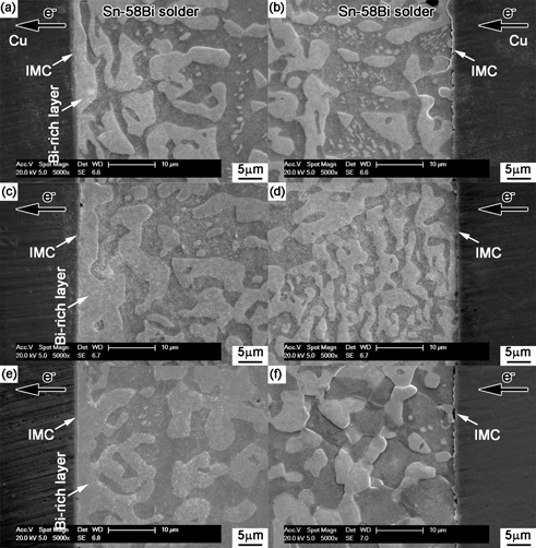
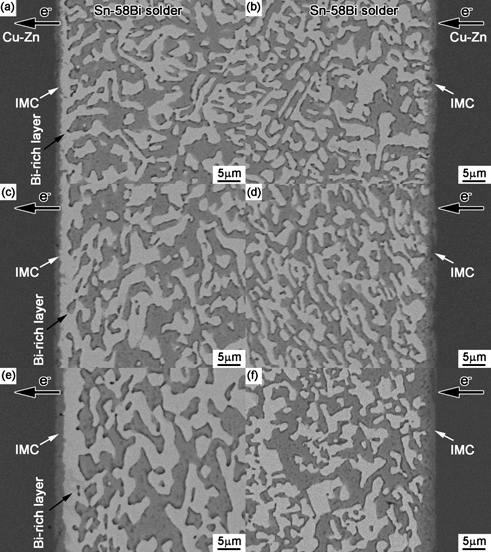
Because the growth of metal hillocks was from the bottom, it was necessary to investigate their interior microstructure and its relationship with the stressing time. The samples with electromigration were polished and observed with SEM. Figures 6 and 7 show the interfacial structures in Sn-Bi/Cu and Sn-Bi/Cu-Zn joints after current stressing for 33 h, 66 h and 132 h, respectively. The left- and right-column also represent the anode side and cathode side, respectively. It can be observed that massive Bi atoms were accumulated at the anode side to promote Bi segregation and the formation of Bi-rich layer at the anode. With stressing time increasing, more Bi atoms migrated to the anode side to thicken the Bi-rich layer. Meanwhile, the thickness of IMC layer at anode side increased with the stressing time, while at cathode side, the dissolution of Cu substrate was occurred due to atomic migration from cathode to anode under electromigration and there was no obvious increase on IMC thickness due to the polarity effect from electromigration22).
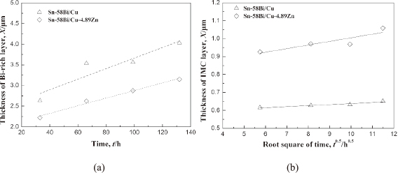
With Zn alloyed into Cu substrate, we can observe the obvious difference on growth thickness of Bi-rich layer and IMC thickness at the cathode side. Figure 8 shows the comparisons on the growth of Bi-rich layer and IMC layer at anode side, in which the thickness was averaged by dividing the total area by the width of area. As observed from the variations in Fig. 8(a), the Bi-rich layer at the anode side grew almost linearly with the current stressing time, but its thickness on Cu-Zn was far thinner than that in Sn-Bi/Cu joint under the same duration of current stressing, which suggests that Zn alloyed into Cu substrate was beneficial to depress the growth of Bi-rich layer at the anode interface for Sn-Bi solder. The thickness of IMC layer at anode side was also measured with the current stressing time. The IMC growth in solder joint usually follows the parabolic model during solid aging or solid current stressing, and follows the empirical diffusion formula:
| \[
X = \sqrt{Dt} + X_{0}
\] | (1) |
where
X is the total IMC thickness,
X0 is the initial IMC thickness,
t is the time and
D is the diffusivity of IMC layer. Therefore, the IMC thickness was plotted with the square root of stressing time with the curve shown in
Fig. 8(b), which really follows a linear regression between them. The result shows that the IMC thickness in Sn-58Bi/Cu-Zn solder joint was little higher than that in Sn-58Bi/Cu joint. The composition of IMC in Sn-Bi solder joints was Cu
6Sn
5, and its growth was mainly attributed to the reaction between Cu atoms diffused from the substrate and Sn atoms from the solder matrix. Correspondingly, thicker Bi-rich layer at the anode side in Sn-Bi/Cu solder joint inhibited the interdiffusion of Sn and Cu atoms, which lead to a relatively thinner IMC layer at the interface.
Electromigration is referred to the mass or atomic transport driven by the combination of thermal and electrical effects. Under the electric current flow, the momentum transfer from electrons to atoms usually drives atoms from the cathode to the anode and vacancies from the anode to the cathode. With more solder atoms driven into the anode and vacancies into the cathode, a very high compressive stress and tensile stress will be produced in the region at the anode and the cathode, respectively, which will result in the formation of protrusion or hillocks at anode and depletion or voids at cathode due to the stress releasing, as seen in Fig. 4 on Cu/Sn-58Bi/Cu joints and Fig. 5 on Cu-Zn/Sn-58Bi/Cu-Zn joints. At the anode side, the relationship between the exterior hillocks or whiskers and interior Bi-rich layer must be considered. In Figs. 6 and 7, the formation of Bi-rich layer at the anode indicated that Bi atoms migrated with the electron flow. The compressive stress formed at the anode side due to the excessive atomic accumulation when the Bi atoms migrated toward the anode side. On the contrary, tensile stress formed at the cathode side due to the atomic departure. The compressive stress at the anode increased with the migration of Bi atoms into the anode region, and then finally released with the protrusion of hillocks or whiskers at the anode region. EDX confirms that the composition of whisker in Fig. 5(c) is 91.1 mass% Sn, 2.1 mass% Cu and 6.8 mass% Bi, which is a typical Sn whisker. The formation of Sn whisker at the anode area is helpful to release the compressive stress and also important to provide the crystal sites for the incoming Bi atoms during electromigraiton. On the other hand, due to the gradient on vacancy concentration, back stress will be produced between the tensile cathode region and the compressive anode region, which retards the atomic transport during electromigration. Therefore, the atomic diffusion flux J occurred in electromigration can usually be expressed by23):
| \[
J = J_{\rm em} + J_{\sigma} = {\rm CD}/kT (eZ^{*} \rho j - \Omega \partial\sigma/\sigma x)
\] | (2) |
where
Jem is the mass flux resulted from electron wind force,
Jσ is the mass flux resulted from back stress,
C is the concentration of Bi in the Sn-Bi eutectic solder,
k is Boltzmann constant,
T is the absolute temperature,
e is the electronic charge,
Z* is the effective charge number,
ρ is the electrical resistivity,
j is the current density, Ω is the atomic volume, and
$\partial\sigma /\sigma x$ is the stress gradient.
The formation of hillocks and whiskers at the anode interface and the formation of depletion or voids at the cathode interface are the common phenomena in Sn-solder with Cu or Cu-Zn substrate. However, what's the important things are the differences on the surface flatness and thickness of Bi-rich layer caused from Zn alloying Cu substrate. The relative flatter surface in solder matrix and thinner Bi-rich layer at anode interface represent that the rate of electromigration in the Sn-Bi/Cu-Zn joint is slower than that in the Sn-Bi/Cu joint. Ouyang et al.24) pointed out that the difference on surface flatness reflected the difference on local vacancy distribution in the solder joints during electromigration. In Sn-58Bi/Cu solder joints, the apparent unevenness on surface morphology illustrated that large amounts of lattice sites were depleted at the cathode side by vacancy absorption and created at the anode side by vacancy annihilation, respectively. Besides through the hillocks and whiskers at the anode interface and the depletion or voids at the cathode interface, the stress release was also occurred through the protrusion of grains in the solder matrix. In Fig. 4, the protrusion of Sn grains almost covers the whole surface. Sn grains were considered to be favorable sites for stress releasing instead of Bi grains due to the difference on the crystal structure of Sn and Bi. The crystal structure of Sn and Bi belongs to a body-centered tetragonal and rhombohedral structure, respectively. The former structure shows an easier plastic deformation during creep. Therefore, the back stress was reduced due to the adequate release under electromigration in the Sn-Bi/Cu solder joints. Accordingly, large amounts of Bi atoms were migrated into the anode region to promote a thicker Bi-rich layer at the anode interface. However, in Sn-58Bi/Cu-Zn solder joints, the relative flat surface means less absorption or annihilation of vacancies during electromigration. Therefore, there existed a high back stress in the solder joints, and so the retardation on atomic migration from back stress increased. The possible reason may be attributed to the existence of Zn atoms. During soldering, Zn atoms from the Cu-Zn substrate was dissolved into interfacial Cu6Sn5 IMC and also diffused into the liquid Sn-58Bi solder matrix. During electromigration, the continuous growth of IMC layer at the anode interface and the dissolution of IMC layer at the cathode further released Zn atoms to the solder matrix. It is well known that the flow of Zn atoms was from the anode side to the cathode side under a higher back stress25), which was opposite to the direction of Bi atoms. Because the migration of Zn atoms to the cathode side would fill the vacancies left behind by the migration of Bi atoms, it was helpful to slow the diffusion of Bi atoms to the anode and the formation of Bi-rich layer at the anode side.
This retarding effect can be estimated by the mass flux of Bi atoms induced by electromigration. Chen et al.26) proposed that the EM-induced atomic flux of Bi can be calculated by:
| \[
J_{\rm em} = v_{\rm Bi} \times d \times ({\rm N}/{\rm m}) \times 57\%
\] | (3) |
Where vBi is the accumulation rate of Bi-rich layer, d is the density of Bi (9.8 g/cm3), N is the Avogadro's number (6.02 × 10²³ atoms/mol), and m is the atomic weight of Bi (208.98 g/mol). The average accumulation rate of Bi-rich layer in Sn-Bi/Cu and Sn-Bi/Cu-Zn is 4.65 × 10⁻⁵ μm/s and 2.79 × 10⁻⁶ μm/s, respectively. According to eq. (3), Jem can be calculated to be 1.31 × 10¹⁴ atoms/cm2·s and 7.88 × 10¹² atoms/cm2·s. From eq. (2), the product of the diffusivity and the effective charge number DZ*, can be calculated as the following equation:
| \[
DZ^{*} = J_{\rm em}kT/e\rho jc
\] | (4) |
It should be mentioned that the real temperature on sample measured by thermal couple was about 15℃ higher than the room temperature due to the effect of Joule heating. Therefore, by substituting k = 1.38 × 10⁻²³ J/K, e = 1.6 × 10⁻¹⁹ C, ρ = 30 × 10−6 Ω·cm, j = 1.0 × 10⁴ A/cm2, C = 1.41 × 10²² atoms/cm3, the DZ* in Sn-58Bi solder with the Cu and Cu-4.89Zn substrate is about 3.69 × 10⁻¹¹ cm2/s and 1.76 × 10⁻¹¹ cm2/s, respectively. Sn-58Bi solder with Cu-Zn shows a smaller DZ*.