Effects of Dynamical Electron Diffraction on Phase Shift Detected by Electron Holography
2019 Volume 60 Issue 10 Pages 2120-2124

Details
2019 Volume 60 Issue 10 Pages 2120-2124
Recently, the effect of dynamical electron diffraction on the phase shift in electromagnetic field analysis using transmission electron microscopy has become increasingly important. In the present study, we investigated the effect of dynamical electron diffraction on the phase shift in electron holograms recorded from a wedge-shaped specimen of single-crystal Si around a Bragg diffraction condition. The results show that the effective inner potential depends on the direction of the incident electron beam, especially near Bragg conditions. The characteristic phase shift was analyzed using dynamical electron diffraction theory (Bethe method).
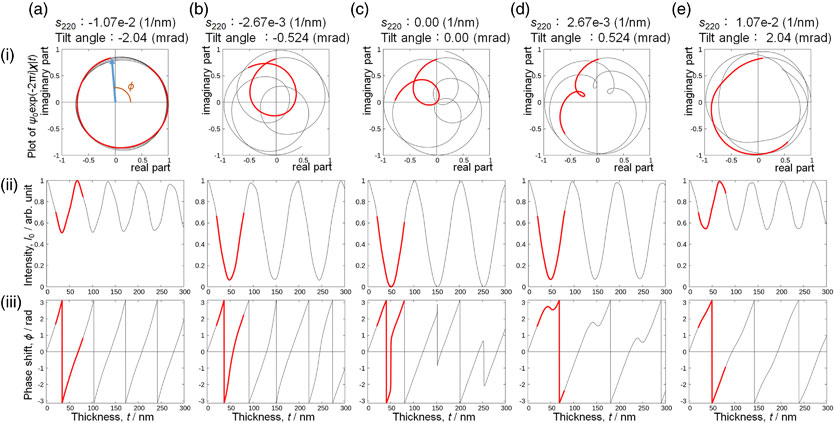
Fig. 1 Multi-beam dynamical electron diffraction theory (Bethe method) calculations. The columns (a)–(e) show different diffraction conditions. (i) The complex value $\psi _{0}\exp ( - 2\pi i|\boldsymbol{{\chi|t}})$ plotted on a complex plane with thickness as a parameter. (ii) Intensity and (iii) phase shift plotted as a function of thickness. The data from 20 nm to 80 nm are plotted by red bold lines.
With recent improvements in the precision and sensitivity of electromagnetic field analysis using transmission electron microscopy, such as electron holography,1–3) DCP-STEM4) and electron diffractive imaging,5) the effect of dynamical electron diffraction on the phase shift ϕ has become important. Generally, the phase shift of an electron beam passing through an electrical potential φ is described by
| \begin{equation} \phi (x,y) = \sigma \int \varphi (x,y,z)dz \end{equation} | (1) |
| \begin{equation*} \sigma = \frac{2\pi}{\lambda E(1 + \sqrt{1 - \beta^{2}})} \end{equation*} |
For the phase shift of an electron beam, the solution of the Howie–Whelan equations14) for the two-beam approximation of dynamical theory gives a qualitative solution. Near the Bragg condition, two Bloch waves with slightly different wavelengths are excited, and the excitation rate depends on the incident beam direction. However, the solution of the Howie–Whelan equation includes many approximations ignoring phase terms to ensure intensity, and we therefore selected to use the Bethe method,15–22) which is a multi-beam dynamical diffraction theory, for a quantitative analysis of the phase shift.
According to the dynamical theory of electron diffraction (Bethe method), the wave function ψ0 of a transmitted electron beam (which corresponds to the object wave in the term of electron holography) that propagates a distance t in a crystal specimen is expressed by a linear combination of Bloch waves, as follows:23)
| \begin{align} \psi_{0} & = \sum_{j}\alpha^{(j)}C_{0}^{(j)}\exp (2\pi i|k^{(j)}|t)\\ & = \sum_{j}\alpha^{(j)}C_{0}^{(j)}\exp (2\pi i(|K| + \gamma^{(j)})t)\\ & = \exp (2\pi i|K|t)\sum_{j}\alpha^{(j)}C_{0}^{(j)}\exp (2\pi i\gamma^{(j)}t) \end{align} | (2) |
| \begin{equation} I_{0} = \psi_{0}\psi_{0}^{*} = \left|\sum_{j}\alpha^{(j)}C_{0}^{(j)}\exp (2\pi i\gamma^{(j)}t)\right|^{2} \end{equation} | (3) |
The phase shift ϕ is the difference between the phase of an object wave (eq. (2)) and the phase of a reference wave. The phase of the reference wave is expressed by $2\pi |\boldsymbol{{\chi|t}}$, where $\boldsymbol{{\chi}}$ is the wave vector of an electron in vacuum. Therefore, ϕ can be calculated using the following formula;
| \begin{align} \phi & = \text{angle}\{\psi_{0}\exp (- 2\pi i|\chi |t)\}\\ & = \text{angle}\Biggl[\Biggl\{\exp (2\pi i|K|t)\sum_{j}\alpha^{(j)}C_{0}^{(j)}\exp (2\pi i\gamma^{(j)}t) \Biggr\}\\ &\quad \times \exp (- 2\pi i|\chi |t) \Biggr]\\ & = \text{angle}\left\{\exp (2\pi i(|K| - |\chi |)t)\sum_{j}\alpha^{(j)}C_{0}^{(j)}\exp (2\pi i\gamma^{(j)}t) \right\}\\ & = \text{angle}\left\{\exp \left(i\sigma \int_{0}^{t}V_{0}dt\right)\sum_{j}\alpha^{(j)}C_{0}^{(j)}\exp (2\pi i\gamma^{(j)}t) \right\} \end{align} | (4) |
To simulate the intensity and phase shift of the transmitted beam, nine beams in a 220 systematic row (000, 220, 440, 660, 880, -2-20, -4-40, -6-60, -8-80) are considered in our calculations. The effects of absorption of intensity are not considered. We developed a code to calculate the dynamical electron diffraction using the Bethe method including an external subroutine that yields the atomic form factors for electron diffraction.24) The value of V0 of Si used in our code is 11.5 V.25)
2.2 Experimental procedureA TEM specimen was prepared from a Si (100) wafer using a focused ion beam (FIB) milling system (JIB-45000 MultiBeam, JEOL). The wedge angle, which was controlled by FIB, was about 52°. Electron holography was performed using a 300-kV TEM system (JEM-3000F, JEOL) equipped with a single biprism. The holograms were recorded under a two-beam condition (transmitted beam and 220 reflection). The incident beam direction was controlled using a beam tilt function.
Figure 1 shows the results of a calculation of the dynamical theory of electron diffraction. The columns (a)–(e) show different diffraction conditions. The upper row (i) shows plots of $\psi _{0}\exp ( - 2\pi i|\boldsymbol{{\chi|t}})$ on a complex plane with thickness as a parameter (refer eq. (4)). The range of the thickness is from 0 nm to 300 nm. The data from 20 nm to 80 nm are plotted by red bold lines. To explain Fig. 1(i), a blue vector indicating $\psi _{0}\exp ( - 2\pi i|\boldsymbol{{\chi|t}})$ at 20 nm thickness is drawn in Fig. 1(a-i). The length of the vector corresponds to the square root of the intensity I0, and the angle between the real axis and the vector corresponds to the phase shift ϕ. The middle row (ii) and the lower row (iii) show the intensity and the phase shift plotted as functions of thickness t.

Multi-beam dynamical electron diffraction theory (Bethe method) calculations. The columns (a)–(e) show different diffraction conditions. (i) The complex value $\psi _{0}\exp ( - 2\pi i|\boldsymbol{{\chi|t}})$ plotted on a complex plane with thickness as a parameter. (ii) Intensity and (iii) phase shift plotted as a function of thickness. The data from 20 nm to 80 nm are plotted by red bold lines.
In the center column (Fig. 1(c)), the specimen is under an exact 220 Bragg diffraction condition. In this condition, the trajectory of $\psi _{0}\exp ( - 2\pi i|\boldsymbol{{\chi|t}})$ intersects the origin of the complex plane, as shown in Fig. 1(c-i). At the thickness of the intersection, the length of the vector is zero, so that the corresponding position in the bright-field image shows a dark contrast. It is noted that the direction of the $\psi _{0}\exp ( - 2\pi i|\boldsymbol{{\chi|t}})$ vector is turned over by π across the origin of the complex plane in Fig. 1(c-i). Therefore, the phase shift profile (Fig. 1(c-iii)) shows jumps of π at the dark thickness fringes. In our calculation, those thicknesses are 50.8 nm, 152.0 nm and 253.2 nm. Those thicknesses become close to (1/2 + n)ξ220, because the diffraction condition is almost two beams condition. Here, ξ220 is the extinction distance of 220 reflection, and n is an integer (n ≥ 0). In our calculation ξ220 becomes 108 nm.
The left and right side columns of Fig. 1 show the results when the sign of the excitation error of the 220 reflection s220 is negative and positive, respectively. Figure 1(iii) shows that the gradient of the phase shift depends on the sign of the excitation error s220, i.e. when s220 < 0, the gradient of the phase-shift is high and when s220 > 0, the gradient of the phase-shift is low. This result can be understood by comparing Fig. 1(b-i) and Fig. 1(d-i). In those figures, the trajectory of $\psi _{0}\exp ( - 2\pi i|\boldsymbol{{\chi|t}})$, shown as red bold lines for thicknesses from 20 nm to 80 nm, forms a shape of a small loop. When the sign of s220 is negative (Fig. 1(b-i)), the small loop includes the origin of the complex plane. This means the increase of the phase shift is larger than 2π. When s220 is positive (Fig. 1(d-i)), the small loop does not include the origin of the complex plane, which means the increase of the phase shift is less than 2π. Thus, eq. (4) explains the characteristic phase shift around the Bragg condition that is not explained by eq. (1).
Figure 2 shows bright-field images and reconstructed phase images of a wedge shape Si specimen, and the phase shift profiles in the region of the specimen indicated by the red rectangles in the bright-field and reconstructed phase images. The specimen shown in Fig. 2(a) is under a non-Bragg condition and that shown in Fig. 2(b) is under an exact 220 Bragg diffraction condition. Under the non-Bragg condition, there are no thickness fringes in the bright field image, and the phase shift increases in proportion to the specimen thickness. Under the exact 220 Bragg diffraction condition, thickness fringes appear in the bright-field image, and the phase shift jumps by π (indicated by red arrows in the reconstructed phase image and the phase-shift profile) where the dark thickness fringes appear in the corresponding bright-field image. These π jumps cannot be explained by eq. (1). But they can be explained by dynamical theory of electron diffraction as shown in Fig. 1(c).

Bright-field images, reconstructed phase images, and phase shift profiles of a wedge shaped Si crystal. (a) Strong Bragg reflections are not excited. (b) Bragg diffraction condition with 220 reflection is exactly satisfied. The red arrows indicate the positions of dark thickness fringes. The thicknesses of the positions are about 50 nm and 150 nm which were estimated by our calculations.
Next, we systematically tilted the direction of the incident electron beam around the 220 Bragg diffraction condition using a beam tilt function of the illumination system. The bright field images, the reconstructed phase images and the phase shift profiles for each tilt conditions are shown in Fig. 3(a)–(n). Figures 3(o) and 3(p) are diffraction patterns obtained in the diffraction condition of Figs. 3(a) and 3(n), respectively. From a movement of a cross point of Kikuchi lines indicated by black arrows in Figs. 3(o), (p), the total tilting angle from Fig. 3(a) to 3(n) is estimated to be 5.04 mrad. The tilting was changed in constant steps (0.39 mrad), such that for the tilting condition of Fig. 3(a)–(g), the excitation error of the 220 reflection s220 is negative (which means that the reciprocal lattice point of 220 is located outside the Ewald sphere) and for Fig. 3(h)–(n) s220 is positive (the reciprocal lattice point of 220 is located inside the Ewald sphere). It should be noted that the gradient of the phase-shift against specimen thickness depends on the sign of the excitation error as discussed in the simulation part, i.e., when s220 < 0, the gradient of the phase-shift is high and when s220 > 0, the gradient of the phase-shift is low. The complicated phase shifts near the thickness of (1/2 + n)ξ220, which was expected by the simulation, were also observed experimentally.
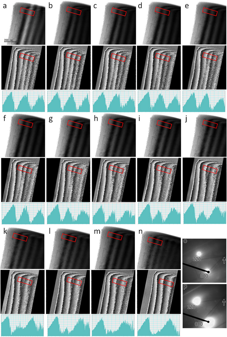
(a)–(n) Tilt series of bright-field images (upper rows), reconstructed phase images (middle rows), and phase shift profiles (lower rows, phase shift (rad) vs. distance (nm)) of a wedge shaped Si crystal around the 220 Bragg diffraction condition. The tilting is changed by a constant step such the excitation error of the 220 reflection s220 ranges from negative in (a)–(g) through to positive in (h)–(n). (o, p) Diffractions patterns obtained in the diffraction condition of (a) and (n). The tilt angle between these two diffraction patterns is estimated from the movement of a cross point of Kikuchi lines, which is indicated by a black arrow, to be 5.04 mrad along an axis perpendicular to a reciprocal lattice vector of 220 reflection.
The complicated phase shifts of an object wave around the Bragg diffraction condition, such as a jump in the phase shift and an effective inner potential depending on the diffraction conditions, were explained by the dynamical theory of electron diffraction. Near a Bragg condition, many Bloch waves with slightly different wavelengths are excited, and the excitation rate of each Bloch wave depends on the incident beam direction. By taking into account the effect of dynamical electron diffraction, the phase-shift map acquired by TEM methods, such as electron holography, DCP-STEM and electron diffractive imaging, can be interpreted quantitatively with high accuracy.
This work was supported by JSPS Grant-in-Aid for Scientific Research No. JP15K06419.