Abstract
Herein, the advantages of high-voltage scanning transmission electron microscopy (STEM) as a tool for structural characterization of micrometer-thick specimens are reported. Dislocations introduced in a wedge-shaped Si crystal were clearly observed by bright-field STEM operating at 1 MV. Many of the dislocations were straight and parallel to the ⟨110⟩, ⟨112⟩ or ⟨113⟩ directions. The widths of the dislocations in the STEM images were almost constant at 13–16 nm (i.e., 4–5 pixels) in the thickness range between 1 and 7.5 µm. The latest high-voltage STEM instrumentation is thus useful for imaging crystal defects in micrometer-thick materials, and enables multi-scale fields of view from a few nanometers squared to over 100 µm2.
1. Introduction
The penetration power of electrons in a specimen has long been an important issue in transmission electron microscopy (TEM) because it closely relates to the propagation mechanism of electrons in a solid as well as its practical importance.1,2) High-voltage electron microscopy (HVEM) is a powerful tool to characterize interior structures and crystal defects in micrometer-thick specimens.3–11) The advantage of HVEM is not only its high penetration power but also its high spatial resolution and multi-scale fields of view. Recently we have demonstrated that the maximum usable (i.e., observable) thickness in HVEM depends on the imaging mode; where a superior usable thickness of 14.7 µm at 1 MV can be obtained with scanning transmission electron microscopy (STEM) compared to that with TEM (5.8 µm at 1 MV).12) The STEM technique has the benefit of being essentially free from the effect of chromatic aberration induced by the imaging lens, which increases its suitability for imaging a thick specimen. Furthermore, the technique is less affected by diffraction contrasts such as thickness contours or bend contours than is true of TEM imaging,13) which is an advantage that can be attributed to the nature of converged electron beam imaging. Hence, as the authors have recently demonstrated, HV-STEM can be a suitable technique to observe an extremely thick specimen. However, examples of the application of HV-STEM for observing thick specimens are limited.12,14–16)
In this paper we show the results of imaging dislocations in a micrometer-thick Si crystal, and the advantages and limitations of the method are given based on the experimental results.
2. Experimental Procedure
Herein, CZ-P Si(110) single-crystal wafers were used. High-density dislocations were introduced into the Si wafers via indentation at room temperature using a micro-Vickers hardness tester (Shimadzu HMV-G20, load: 2 kg, dwell time: 2 s) followed by annealing for 600 s at 1123 K in a high-vacuum furnace (1 × 10⁻⁵ Pa). This technique is effective for generating dislocations from the crack tip as has been reported in the literature,17) where the micro-cracks generated from the corners of the indentation were used. Wedge-shaped specimens were cut from an area in the vicinity of the indentation using a focused ion beam (FIB; Hitachi FB-2000A). Herein, the slope of the wedge-shaped FIB lamella corresponded to the cross-section of the original Si(110) wafer. Further, the shapes of the prepared specimens were characterized by scanning electron microscopy (SEM; Hitachi S-5200) operating at 10 kV.
The dislocations were characterized by bright-field (BF) STEM (JEOL JEM-1000EES) operated at 1 MV. We subjected the specimen to a two-beam condition by exciting the 111 reflection of Si. In the BF-STEM imaging, the beam convergence was set to a semi-angle of 3.75 mrad using a 50 µm condenser aperture and the outer collection angle on the BF detector was set to 13 mrad. Further, a 200-µm-thick P-43 phosphor scintillator was used as the BF-STEM detector. The STEM images 1024 × 1024 pixels in size were acquired with a dwell time of 256–1365 µs/pixel, which depended on the specimen thickness.
3. Results and Discussion
Figure 1(a) shows a plan-view secondary electron (SE) image of a FIB lamella attached to a Cu-grid. A dent-shaped area on the lamella (indicated by a double-arrowhead in Fig. 1(a)) acted as a marker for later HVEM observation. Figure 1(b) shows an SE image viewed in an oblique direction (40° tilt in the SEM), where we can observe that a triangular cross-section was formed, which is suitable for quantitatively determining the specimen thickness. In addition, a micro-crack is present in the middle of the slope (indicated in Fig. 1(b)). In the later HVEM observations, electrons were incident on the crystal from the direction indicated by the vertical arrow in Fig. 1(b). The thickness of the specimen increases from left to right in Fig. 1(b), where the maximum thickness is 9.7 µm at the right side of the crystal. The triangular side-plane of the FIB lamella is almost parallel to the (110) surface of the Si wafer.

Figure 2 shows an overall BF-STEM image of the specimen corresponding to the SE image shown in Fig. 1(a), where the specimen becomes thicker from the left to the right of the image and the dent-shaped marker is indicated (double-arrowhead in Fig. 2). The selected area electron diffraction (SAED) pattern is shown (inset of Fig. 2), where it is seen that the two-beam condition is satisfied. In the BF-STEM image, dislocations are seen as lines with dark contrast in the periphery of the crack, where the contrast of the image was adjusted to clarify the crack and the dislocations. As can be seen, microstructural features of the entire 11 µm × 13 µm specimen are visualized, thus demonstrating the usefulness of BF-STEM to roughly scan the main features of a specimen with a wide field of view greater than 100 µm2.
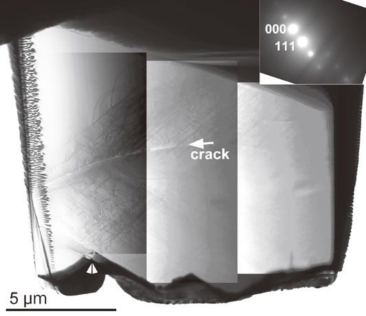
Figure 3 shows a BF-STEM image of a region including high-density dislocations, where the observed area becomes thicker from the left (1.8 µm) to the right (4.4 µm) of the image and the dent-shaped marker is indicated (double-arrowhead in Fig. 3). Most of the dislocations are observed to exhibit line widths of 13–16 nm (i.e., 4–5 pixels with 3.2 nm/pixel). However, the smallest STEM probe size is approximately 1 nm at 1 MV, which limits its resolution. It should be noted that a trade-off exists between resolution and the field of view in STEM imaging. In Fig. 3, the crystallographic orientations are indicated with arrows, and it can be seen that many of the dislocations are straight and parallel to the ⟨110⟩, ⟨112⟩ or ⟨113⟩ directions. Such a directional morphology of dislocations can be attributed to deep valleys in the Peierls-Nabarro (P-N) potential of the Si crystal.18,19) However, some of the dislocations are curved or bend gradually, which is owing to the fact that the P-N force is weakened at high temperatures, and these dislocations were emitted from the crack tip introduced by indentation followed by annealing at 1123 K. Examples of detailed characterization of the dislocations around the crack tip in Si(001) can be found in the literature.20)

Figure 4 shows a composite BF-STEM image including the overall area of the wedge-shaped Si specimen, where the dent-shaped marker is indicated (double-arrowhead in figure). The contrast of each image was adjusted locally to clarify the dislocations, where the specimen becomes thicker from the left (1 µm) to the right (9 µm) of the image. The widths of the dislocation lines are almost constant at 13–16 nm (i.e., 4–5 pixels) in the thickness range between 1 and 7.5 µm. This signifies that a wedge-shaped specimen with a thickness up to 7.5 µm can be observed in focus using 1 MV-STEM. A similar tendency was observed in our previous study, which we attributed to the extended depth of focus of the STEM instrument.12) This illustrates a very important practical advantage of the HV-STEM. Herein, the dislocation lines became blurred and less distinct as the wedge thickness increased to over 8 µm. We note that the maximum usable thickness depends on crystal orientation, where our previous study imaged dislocations in an area over 14 µm thick wherein g(hkl) = 220 was excited.12) Thus we demonstrate herein that HV-STEM is useful for imaging crystal defects in micrometer-thick materials, and enables multi-scale fields of view from a few nanometers squared to over 100 µm2.

4. Conclusion
Herein, visualization of dislocations in a micrometer-thick Si crystal was studied using BF-STEM operated at 1 MV. The obtained results can be summarized as follows;
-
(1)
Dislocations introduced in a wedge-shaped Si crystal were clearly observed by BF-STEM in a two-beam condition exciting the 111 reflection of Si.
-
(2)
Many of the dislocations were straight and parallel to the ⟨110⟩, ⟨112⟩ or ⟨113⟩ directions.
-
(3)
Widths of the dislocation lines were almost constant at 13–16 nm (i.e., 4–5 pixels) in the thickness range between 1 and 7.5 µm.
-
(4)
The latest HV-STEM instrumentation is useful for imaging crystal defects in micrometer-thick materials, and enables multi-scale fields of view from a few nanometers squared to over 100 µm2.
Acknowledgments
The authors wish to thank Mr. A. Ohsaki, Mr. Y. Agatsuma, Mr. S. Takakuwa, Dr. S. Ohta, and Mr. M. Ohsaki of JEOL Ltd for their support using the JEM-1000EES. KS acknowledges Ms. Y. Hiraizumi of Osaka University for technical assistance using FIB. This study was partially supported by the Japan Society for the Promotion of Science (JSPS) Grants-in-Aid for Scientific Research (Grant Nos. JP16K13640 and JP17H02746). We thank Sara Maccagnano-Zacher, PhD for editing a draft of this manuscript.
REFERENCES
- 1) H. Hashimoto: J. Phys. Soc. Jpn. 35 (1964) 277–290.
- 2) H. Fujita and E. Taguchi: Jpn. J. Appl. Phys. 21 (1982) L414–L416.
- 3) H. Fujita, Y. Kawasaki, E. Furubayashi, S. Kajiwara and T. Taoka: Jpn. J. Appl. Phys. 6 (1967) 214–230.
- 4) R. Uyeda and M. Nonomiya: Jpn. J. Appl. Phys. 7 (1968) 200–208.
- 5) C.J. Humphreys, L.E. Thomas, J.S. Lally and R.M. Fisher: Philos. Mag. 23 (1971) 87–114.
- 6) H. Fujita, T. Tabata, K. Yoshida, N. Sumida and S. Katagiri: Jpn. J. Appl. Phys. 11 (1972) 1522–1536.
- 7) G. Thomas and J.-C. Lacaze: J. Microsc. 97 (1973) 301–308.
- 8) A. Takaoka, T. Hasegawa, K. Yoshida and H. Mori: Ultramicroscopy 108 (2008) 230–238.
- 9) Y. Oshima, R. Nishi, K. Asayama, K. Arakawa, K. Yoshida, T. Sakata, E. Taguchi and H. Yasuda: Microscopy 62 (2013) 521–531.
- 10) J. Yamasaki, M. Mutoh, S. Ohta, S. Yuasa, S. Arai, K. Sasaki and N. Tanaka: Microscopy 63 (2014) 345–355.
- 11) S. Sadamatsu, M. Tanaka, K. Higashida and S. Matsumura: Ultramicroscopy 162 (2016) 10–16.
- 12) K. Sato, Y. Yamashita, H. Yasuda and H. Mori: Jpn. J. Appl. Phys. 56 (2017) 100304.
- 13) C.J. Humphreys: Ultramicroscopy 7 (1981) 7–12.
- 14) Y. Nakada, K. Kuroda, T. Kamino, S. Arai, C. Morita and T. Imura: J. Electron Microsc. 34 (1985) 430–434.
- 15) K. Sato, S. Tashiro, Y. Yamaguchi, T. Kiguchi, T.J. Konno, T. Yamamoto, K. Yasuda and S. Matsumura: Mater. Trans. 57 (2016) 918–921.
- 16) T. Fujii, T. Kajita, T. Miyazawa and S. Arai: Mater. Charact. 136 (2018) 206–211.
- 17) M. Tanaka, K. Higashida, K. Kaneko, S. Hata and M. Mitsuhara: Scr. Mater. 59 (2008) 901–904.
- 18) K. Wessel and H. Alexander: Philos. Mag. 35 (1977) 1523–1536.
- 19) Y. Nishino, H. Saka and T. Imura: J. Mater. Sci. 19 (1984) 245–253.
- 20) M. Tanaka, S. Sadamatsu, H. Nakamura and K. Higashida: Mater. Trans. 52 (2011) 352–357.
