Abstract
In our previous study, a thin wire of a Cu–0.29 mass%Zr alloy was produced by annealing after rolling and two subsequent intermediate annealing steps during wire drawing (IA wire). The produced IA wire had an ultimate tensile strength, σu, of 610 MPa and a small total elongation, εt, of 1.2% despite a small grain size, D, of 240 nm. In this study, a thin wire of the same alloy was produced by annealing after rolling and subsequent wire drawing (S wire). Even though the S wire had almost the same values of σu = 620 MPa and D = 230 nm as the IA wire, the S wire exhibited a larger εt = 2.9%. This study investigated the cause of this smaller value of εt for the IA wire. In both the IA and S wires, voids were formed by decohesion of the interface between the Cu matrix and particles consisting of a eutectic (Cu + Cu5Zr) during wire drawing; however, the fraction of eutectic particles with voids was larger in the IA wire than the S wire. The IA wire exhibited lower ductility as a result of easier coalescence of the voids during tensile testing. In addition, the larger fraction of eutectic particles with voids in the IA wire is attributed to the larger size of recrystallized grains generated by the intermediate annealing during wire drawing than that of the grains before intermediate annealing. As a result, dislocations accumulated significantly around the eutectic particles during the subsequent wire drawing, resulting in a high stress concentration.
This Paper was Originally Published in Japanese in J. Japan Inst. Copper 59 (2020) 76–79. The captions of all figures and table have been modified slightly.
1. Introduction
In recent years, the extreme thinning of copper-alloy wires used for parts such as electronic devices has accelerated. As a result, the wires require not only high conductivity but also appropriate strength to prevent breakage.
Recently, Muramatsu et al. conducted a series of studies on hypoeutectic Cu–0.72–7.2 mass%Zr (hereinafter mass% will be omitted in the notation) alloy wires fabricated by vertical upward continuous casting (VUCC) followed by wire drawing.1–3) In general, increasing the Zr concentration led to higher strength and lower conductivity of the hypoeutectic Cu–Zr alloys. They reported that the Cu–7.2Zr alloy wire showed a high tensile strength, σu, of 2.2 GPa, and the Cu–0.72Zr alloy wire exhibited a high electrical conductivity, E, of 83% IACS.
However, alloy wires for applications such as power transmission cables are required to possess a high electrical conductivity of 90% IACS or greater. To further improve the electrical conductivity of Cu–Zr alloy wires processed by wire drawing, Muramatsu et al. conducted tandem rolling and subsequent wire drawing with repeated intermediate annealing followed by the final wire drawing for a Cu–Zr alloy having a low Zr concentration of 0.29% produced by VUCC.4) The fabricated wire had σu = 610 MPa, a large value of E = 91% IACS, and a small total elongation, εt, of 1.2%. However, the reason for the low ductility of the wire was not elucidated.
Nomura et al. performed equal channel angular pressing (ECAP)-conform processing, which involved severe plastic deformation, before tandem rolling and wire drawing with the aim of improving the strength and ductility of a Cu–0.29Zr alloy wire through grain refinement.5) ECAP-conform processing is a combinational method consisting of a conform process and ECAP. The wire fabricated by the ECAP-conform processing with subsequent rolling and wire drawing showed a good balance of strength (σu = 790 MPa) and ductility (εt = 3.9%) through grain refinement. However, the electrical conductivity of the wire decreased from 88% IACS after the ECAP-conform processing to 73% IACS after wire drawing.
In our previous study,6) we investigated the cause of the decrease in electrical conductivity with tandem rolling and wire drawing after ECAP-conform processing. Fine spherical precipitates with an ordered face-centered cubic (fcc) lattice and a cube-on-cube orientation relationship to the Cu matrix were formed during casting7) and ECAP-conform processing due to the heat generated during processing. It was revealed that the fine spherical precipitates were sheared by dislocations during rolling and wire drawing, resulting in an increase in Zr concentration as solid-solution atoms in the Cu matrix.
In the present study, the cause of the low ductility of an intermediate-annealed Cu–0.29Zr alloy wire is investigated through detailed microstructural observations considering previous results6) by comparing Cu–0.29Zr alloy wires subjected to three different processing routes: tandem rolling and wire drawing with repeated intermediate annealing (route 1), rolling and wire drawing after ECAP-conform processing (route 2), and wire drawing after rolling and subsequent annealing (route 3).
2. Experimental Procedure
As previously detailed by Nomura et al.,5) a Cu–0.29Zr alloy rod with a diameter, d, of 14 mm produced by VUCC was subjected to conform extrusion to d = 10 mm, followed by ECAP-conform processing four times. Subsequently, the Cu–0.29Zr alloy rod with d = 10 mm was subjected to tandem rolling to d = 3 mm, followed by wire drawing to d = 0.2 mm. Specimens obtained after the ECAP-conform processing (route 2) are collectively referred to as “ECAP wire”. For the specimens obtained through route 3, a cast Cu–0.29Zr alloy was machined to d = 10 mm and then tandem-rolled to d = 5 mm with subsequent annealing, followed by final wire drawing to d = 0.2 mm. In addition, the machined cast Cu–0.29Zr alloy with d = 10 mm was tandem-rolled to d = 5 mm with subsequent annealing, and then wire drawing and annealing were repeated twice. Finally, the annealed wires with d = 1 mm were drawn to d = 0.2 mm (route 1). Hereafter, the wires obtained through routes 3 and 1 are collectively referred to as “S wire” and “IA wire”, respectively. Furthermore, for example, a wire with d = 0.6 mm is expressed as “0.6ECAP wire”, “0.6S wire”, or “0.6IA wire”. All of the annealing processes mentioned above were carried out at 650°C for 1 h.
Microstructural observations were performed using a transmission electron microscope (TEM: Tecnai G2 30, FEI, Hillsboro, OR, USA) and a field-emission scanning electron microscope (FE-SEM: JSM-7100F, JEOL, Tokyo, Japan). To prepare the TEM specimens, the wires were polished into strips with a thickness of 100 µm, followed by ion beam processing at a voltage of 5.0 kV using an ion slicer (EM-09100IS, JEOL, Tokyo, Japan). However, wires with a diameter of less than approximately 0.5 mm were too small to obtain TEM specimens. To prepare the specimens for SEM observations, the wires were embedded in thermosetting resin, polished, and buffed with alumina abrasives to obtain mirror surfaces. Then, the SEM specimens were polished using a Struers automatic polishing machine with 80 mL of OP-S solution containing colloidal silica particles having a diameter of 40 nm and containing several drops each of hydrogen peroxide solution and 25% aqueous ammonia. The average grain sizes of the wires were measured from backscattered electron (BSE) images using the linear intercept method.
The dislocation density was evaluated by X-ray diffraction (XRD) using an X-ray diffractometer (RINT-2500, Rigaku Corporation, Tokyo, Japan) with Cu-Kα radiation. The modified Williamson–Hall method8) was used to estimate the dislocation densities by converting the amount of strain calculated from the full widths at half maximum (FWHM) of the X-ray diffraction peaks corresponding to the (111), (200), (220), and (311) planes.
Tensile tests of the drawn wires were performed at room temperature using a universal testing machine (AUTOGRAPH AG-I, Shimadzu, Kyoto, Japan) with a distance of 100 mm between the grippers at a strain rate of 1.7 × 10⁻⁴ s−1 (cross-head speed of 1 mm/min). The electrical conductivities of the wires were determined as E = (ρ0/ρ) × 100 with a resistivity, ρ0, of 17.2 nΩm for pure copper by measuring the resistivity, ρ, of the wires through the four-terminal method.
3. Results and Discussion
The average grain size of the cast Cu–0.29Zr alloy was 13 µm. SEM observations of the cast alloy reveal a granular eutectic composed of Cu and Cu5Zr with an average diameter of approximately 1.5 µm inside the grains and a plate-shaped eutectic with a length of approximately 10 µm at the grain boundaries.6)
Figure 1 shows the average grain size, D, of the IA, S, and ECAP wires as a function of the inverse of the diameter, d−1. TEM observations after the conform extrusion or ECAP-conform processing reveal the existence of recrystallized grains in part of the overall microstructures of both wires.6) The average grain size, D, of the ECAP wire before wire drawing was refined to 0.9 µm in route 2.6) As shown in Fig. 2, because the grains were elongated in the rolling or wire drawing direction by the tandem rolling or wire drawing, the average spacing of the grain boundaries parallel to the rolling or wire drawing direction was measured as D. The solid black circles in Fig. 1 indicate the D values of the recrystallized grains generated by the annealing processes. In all specimens, the value of D was decreased by rolling or wire drawing and increased by recrystallization in the IA and S wires.


Table 1 summarizes the ultimate tensile strength, σu; total elongation, εt; dislocation density, ρ; average grain size, D; and conductivity, E, of the 0.2S, 0.2IA, and 0.2ECAP wires. Here, 0.2 denotes the diameter, d, of the wires. The data for the 0.2IA and 0.2ECAP wires were taken from our previous study.6) In our previous study,6) it was shown that the difference in yield strength between the 0.2ECAP and 0.2IA wires was mainly caused by differences in the amounts of dislocation strengthening and grain-boundary strengthening. Based on the results of the previous study,6) it is easily imagined that the difference in yield strength between the 0.2S and 0.2ECAP wires or between the 0.2S and 0.2IA wires can also be attributed to differences in the amounts of the above-mentioned strengthening. As presented in Table 1, the ECAP wire exhibited the highest strength among the three types of specimens. It is inferred that this result was caused by the highest ρ and smallest D values for this specimen. Thus, the reason that the 0.2IA and 0.2S wires exhibit almost the same strength should be because the ρ and D values of these wires are almost the same. However, it should be noted that the value of εt for the 0.2IA wire is lower than that for the 0.2S wire, although the values of σu, ρ, and D are nearly equal for the 0.2IA and 0.2S wires. This indicates the existence of other factors besides D and ρ that affect the value of εt.

Table 1 Ultimate tensile strength (σu), total elongation (εt), dislocation density (ρ), average grain size (D), and electrical conductivity (E) of the 0.2S, 0.2IA, and 0.2ECAP wires.
Therefore, to investigate the cause of the low ductility of the 0.2IA wire, the fracture surfaces of the three types of wires were observed after the tensile tests. Figure 3 shows an SEM image of a typical fracture surface of the 0.2IA wire. As dimple patterns were observed on the fracture surfaces in all of the wires, the fracture behavior of the wires was ductile fracture. In addition, spherical particles with a diameter of approximately 2 µm were present at the bottom of approximately half of the dimples, as indicated by the arrows. These observation results indicate that voids were formed by decohesion at the interface between the particles and the Cu matrix, and their growth and coalescence led to the fracture of the wires. Figure 4 displays an SEM image of the vertical cross-section of the 0.2IA wire. The spherical particle observed in Fig. 4 is eutectic and consists of Cu5Zr and Cu.7) Hereinafter, the spherical particles are referred to as eutectic particles. As shown in Fig. 4, voids formed by decohesion at the eutectic particle/Cu matrix interfaces were already present before tensile tests for all of the wires. Thus, it appears that the eutectic particles were formed during the wire drawing process from the spherical eutectic itself inside the grains or the plate-shaped eutectic at the grain boundaries observed in the cast Cu–0.29Zr alloy.

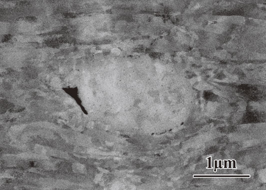
Figure 5 shows the fraction, fe, of eutectic particles with voids as a function of d−1 for the IA, S, and ECAP wires. For the ECAP and S wires, the value of fe increased and became saturated with increasing d−1. The value of fe was saturated when d−1 ≥ 1/3 mm−1, and d−1 ≥ 1/0.6 (= 5/3) mm−1 for the ECAP and S wires, respectively. It can be considered that the value of fe was almost saturated when d−1 = 1/0.2 (= 5) mm−1 for the IA wire. Table 1 indicates that the value of εt decreased in the order of 0.2ECAP, 0.2S, and 0.2IA wires, whereas the value of fe increased in this order. This indicates that the presence of voids in the wires before the tensile tests is a key factor influencing the ductility. Therefore, because the value of fe is the largest for the 0.2IA wire, the growth and coalescence of voids will occur most easily during the tensile test in the 0.2IA wire, resulting in the smallest value of εt.

Finally, the reason that the 0.2IA wire had the highest value of fe is considered. Before reaching the saturated value of fe in Fig. 5, accumulated dislocations were observed around eutectic particles inside grains larger than roughly 1 µm after rolling or annealing with subsequent wire drawing. Analyses of selected-area electron diffraction patterns and Kikuchi lines revealed that there was a misorientation of approximately 2° to 3° between the regions with and without the accumulated dislocations. An example of the accumulation of dislocations around a eutectic particle is shown in Fig. 6(a). The formation of voids became easier as a result of the significant stress concentration caused by the accumulation of dislocations during rolling and wire drawing. On the other hand, after reaching the saturated value of fe, the grain size decreased to approximately 0.4 µm or less, as shown in Fig. 1. In this case, as seen in Fig. 6(b), dislocations were not particularly accumulated around the eutectic particles but were densely and uniformly distributed in the overall microstructure. Correspondingly, there was no particular difference in the misorientation between the vicinity of the eutectic particle and the region away from the particle in each grain. These results indicate that no significant stress concentration occurred around the eutectic particles, resulting in the suppression of void formation. Therefore, the easiest formation of voids at the eutectic particle/Cu matrix interface in the IA wire can be attributed to the development of a large stress concentration due to accumulated dislocations around the eutectic particles during wire drawing after intermediate annealing, which produced large recrystallized grains.

4. Conclusions
-
(1)
A thin Cu–0.29 mass%Zr alloy wire was produced by tandem rolling with annealing, followed by repeated wire drawing and annealing twice and a final wire drawing (IA wire). In addition, a thin wire of the alloy was produced by rolling with annealing followed by wire drawing (S wire). The 0.2IA wire exhibited almost the same grain size of 240 nm and tensile strength of 610 MPa as the S wire; however, the 0.2IA wire with an elongation of 1.2% was less ductile than the 0.2S wire with an elongation of 2.9%.
-
(2)
Voids were generated by decohesion at the interface between the Cu matrix and eutectic particles due to the wire drawing. The fraction of eutectic particles with voids in the 0.2IA wire was higher than that in the 0.2S wire. The lower ductility of the 0.2IA wire is attributable to the higher possibility of void coalescence during tensile tests.
-
(3)
In the IA wire, voids were more easily formed at the eutectic particle/Cu matrix interfaces during wire drawing than in the S wire. This is ascribed to the generation of large recrystallized grain during intermediate annealing in the wire drawing process, in which dislocations accumulate around the eutectic particles during subsequent wire drawing, resulting in significant stress concentration.
Acknowledgments
This research was supported by a Grant-in-Aid for the 2017–2018 academic year from the Japan Institute of Copper.
REFERENCES
- 1) H. Kimura, A. Inoue, N. Muramatsu, K. Shin and T. Yamamoto: Mater. Trans. 47 (2006) 1595–1598.
- 2) N. Muramatsu, H. Kimura and A. Inoue: Mater. Trans. 53 (2012) 1062–1068.
- 3) N. Muramatsu, H. Kimura and A. Inoue: Mater. Trans. 54 (2013) 176–183.
- 4) N. Muramatsu, T. Nakajima, T. Fukuoka and R. Monzen: J. Japan Inst. Copper 56 (2017) 39–44.
- 5) K. Nomura, T. Nakajima, N. Muramatsu, H. Watanabe and R. Monzen: J. Japan Inst. Copper 57 (2018) 107–111.
- 6) H. Watanabe, K. Miyamoto, T. Kunimine, R. Monzen, N. Muramatsu, K. Nomura and S. Ueno: J. Japan Inst. Copper 58 (2019) 7–12.
- 7) K. Nakashima, K. Miyamoto, T. Kunimine, R. Monzen and N. Muramatsu: J. Alloys Compd. 816 (2020) 152650.
- 8) T. Kunieda, M. Nakai, Y. Murata, T. Koyama and M. Morinaga: ISIJ Int. 45 (2005) 1909–1914.

