Abstract
The number of radio systems used for global communications or advanced features is increasing in electronic devices such as smart phones. As mobile information and telecommunications terminals are miniaturized and advanced features are added by manufacturers, measures to prevent electromagnetic interference among electronic components on high-density mounting boards are becoming increasingly important. Therefore, it is crucial to develop methods for forming electromagnetic wave shield films in semiconductor devices. Stable sputtering processes are increasingly used for the deposition of shield films. Although metal is often used as a shield film, the mechanism of the adhesion of the sputtered film to the mold resin in semiconductor devices has not been discussed. In this work, sputtering was used to deposit a stainless steel film as a ground film for a copper wave shield film and the factors that affected the adhesion of the stainless steel film to the mold resin were investigated. For the copper film with no ground film, adhesion decreased as the resin filler content decreased. For the copper/stainless steel film, adhesion remained high as the filler content of the mold resin decreased. The argon and nitrogen plasma etching formed carbides and nitrides at the interface of the mold resin and a stainless steel film, whereas argon etching formed carbides. Based on the experimental results, we proposed that the adhesion between the stainless steel film and the mold resin mainly arose from the carbides and nitrides reacting with iron and chromium in the stainless steel film.

1. Introduction
In recent years, the number of radio systems used for communication and advanced features in electronic devices such as smartphones is increasing. The clock frequency and data communication rate of circuits have also increased and often generate noise in the same frequency bands as those used for radio systems. The noise emitted by semiconductor devices on high-density mounting boards causes electromagnetic interference,1,2) which must be reduced by blocking the noise source and propagation paths. In conventional portable devices, electromagnetic waves are often intercepted by sheet metal shields, where the whole mounting board is enclosed by a metal plate. However, the area required for mounting is large, and this type of shielding has hindered the miniaturization and slimming of electronic devices. Thus, electronics manufacturers increasingly require alternatives to sheet metal shielding to prevent electromagnetic interference in semiconductor device packages.3)
One solution is to use shield packages with an electromagnetic wave shield film formed on the mold resin that encloses a semiconductor device package. Electromagnetic wave shield films can be formed by methods including paste coating, electroless plating, and sputtering.4–14) Sputtering is a particularly cheap and easy method because it is a dry process, although film adhesion is a major problem. The adhesion mechanism has been investigated for films formed by sputtering on a polyimide membrane.15–28) Moreover, for the Ajinomoto build-up film (ABF), the effect of argon plasma pretreatment on the adhesion of a sputtered copper/titanium film has been examined.29) The argon plasma treatment produced nanoscale worm-like surface roughness on the ABF surface, which improved the adhesion of the copper/titanium film, but increasing the plasma output damaged the ABF board. The ABF board consists of silica filler in a polymer resin matrix, and thus strengthening the interface of the film with the filler and matrix may increase the adhesion of the copper/titanium film. The effects of wet-chemical and plasma treatments on the adhesion of electroless and sputter-deposited copper to photodefinable epoxy have also been investigated.30) For the wet chemical treatment, mechanical interlocking adhesion was the main adhesion mechanism. For copper sputtering, oxygen plasma pretreatment achieved the highest tensile strength at the epoxy resin surface. Therefore, increasing the surface contact area by increasing the roughness and surface polarity of the epoxy resin increased adhesion the most. However, few studies have investigated the adhesion of a sputtered metallic film to mold resin. Going forward, semiconductor packages are expected to become slimmer. To reduce warpage of thinner semiconductor packages, it is becoming increasingly common to use smaller amounts of silica fillers in the mold resin. Yet, few studies have considered the adhesion of a sputtered metallic film to mold resin with varying amounts of silica filler.
In this work, we examined the effect of the silica filler content in the mold resin on the adhesion of sputtered copper, stainless steel, and copper/stainless steel films. Stainless steel was chosen because it is cheap, has excellent corrosion resistance, and sufficiently adheres to polyimide when it contains chromium. The effect of etching on the mold resin, the metal-resin interface, and the adhesion were investigated. The factors that affect adhesion were examined to clarify the adhesion mechanism of the sputtered stainless steel film to the mold resin.
2. Experimental Procedure
2.1 Samples
The samples consisted of a biphenyl mold resin containing a silica filler on a wiring substrate with various metallic films deposited by sputtering on the resin surface.
2.2 Sputtering process flow
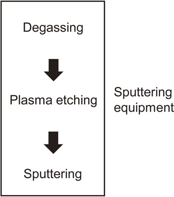
Figure 1 shows the sputtering process flow used in this study. The sputtering equipment consisted of degassing, plasma etching, and sputtering chambers. The degassing chamber removed moisture from the package, the plasma etching chamber etched the mold resin surface of the package to ensure adhesion with the metal film, and the metal films were deposited by sputtering in the sputtering chamber. The ground film was stainless steel 304 and the wave shield film was copper with the high electrical conductivity as an electromagnetic wave shield.
2.3 Process conditions
2.3.1 Filler content of mold resin and adhesion
Film adhesion was measured for filler content of 88%, 78%, and 60%. The degassing conditions are shown in Table 1 and the sputtering conditions are shown in Table 2. The shield films consisted of either copper or copper/stainless steel. The stainless steel film thickness was 0.1 µm. The etching power was 800 W, the argon flow was 9.0 × 10⁻³ m3/h, the nitrogen flow was 9.0 × 10⁻³ m3/h, and the etching time was 300 s.

Table 1 Degassing conditions.

Table 2 Sputtering conditions.
The effect of the etching conditions on the filler exposure ratio was examined with the filler content fixed to 88%. The degassing conditions are shown in Table 1 and sputtering conditions are shown in Table 2. Table 3 shows the etching conditions and the filler exposure ratio. The shield films consisted of either copper or copper/stainless steel. The stainless steel film thickness was set as 0.1 µm.
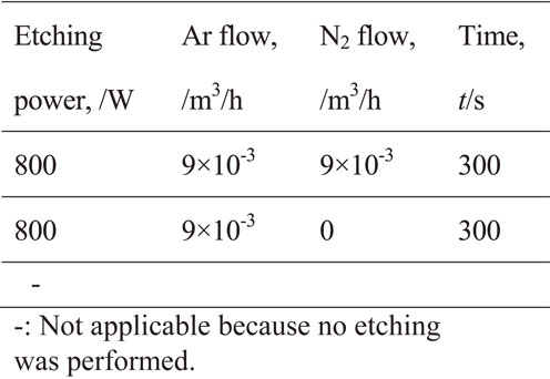
Table 3 Etching conditions.
The effect on film adhesion of the film composition, the stainless steel film thickness, and the etching conditions were evaluated at a filler content of 88%. The degassing conditions are shown in Table 1 and sputtering conditions are shown in Table 2. The shield films consisted of either copper or copper/stainless steel, the stainless steel film thicknesses were 0.1, 0.2, and 0.3 µm, and the etching conditions are shown in Table 4.
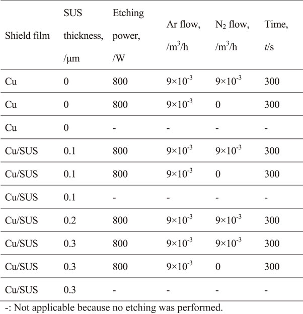
Table 4 Film composition, film thickness, and etching conditions.
Adhesion was tested using the American Society for Testing and Materials cross-cut method.31) The test was performed as follows. Eleven parallel cuts were made at 1 mm intervals, followed by 11 more cuts that intersected the first cuts at 90° (creating a total of 100 grid cells). Adhesive tape (Elcometer 99, Elcometer; adhesive force: 5.59 N/cm) was applied and peeled off in the 180° direction. The evaluation index was the peeling ratio, calculated as the percentage of the 100 grid squares that peeled off when the tape was removed. Adhesion was tested after moisture absorption resistance reflow (moisture absorption conditions: 85°C, 75%, 24 h; reflow conditions: 260°C peak × 5) and was determined from the peeling ratios of 10 samples.
2.4.2 Filler exposure ratio
Etching the mold resin exposed the silica filler at the mold surface, which was expected to affect adhesion. Therefore, the amount of exposed silica filler at the mold surface was measured by binarizing scanning electronic microscopy (SU8040, Hitachi High Technology).
2.4.3 X-ray photoelectron spectroscopy
To explore the adhesion mechanism of the mold resin with the copper and stainless steel films, the interface was analyzed by X-ray photoelectron spectroscopy (Quantera SXM, PHI). Copper and stainless steel films 10 nm thick were formed on the mold resin, and it was scanned and measured in the depth direction from the metal side. The degassing conditions are shown in Table 1. Sputtering conditions were the same as those in Table 2, except for the film thickness. The shield film compositions and etching conditions of the samples are shown in Table 5. The area of X-ray irradiation was 100 µm in diameter.

Table 5 Film composition and etching conditions of X-ray photoelectron spectroscopy samples.
3. Results
3.1 Relationship between filler content and film adhesion
The effect of the filler content on adhesion was examined by using the cross-cut method to measure the film peeling ratio at various filler contents (Fig. 2). For the copper film, the peeling ratio increased as the filler content decreased. At a filler content of 60%, the peeling ratio was 100%. For the copper/stainless steel film, at filler content of 88% and 78%, the peeling ratio was 0%. At a filler content of 60%, the peeling ratio increased slightly to 3%, but it did not change sharply. Compared with the copper film, the adhesion of the copper/stainless steel film with the mold resin was better.
3.2 Filler exposure ratio and adhesion
The filler exposure ratio was altered by changing the etching conditions and the film adhesion was measured by the peeling ratio using the cross-cut method (Fig. 3). With no etching, no filler was exposed and the peeling ratio was 100% for the copper film and the copper/stainless steel film. Argon plasma etching achieved a filler exposure of 4.4%. For the copper film, the peeling ratio was 100%, whereas that for the copper/stainless steel film was only 1.5%. Argon and nitrogen plasma etching achieved a filler exposure ratio of 38%, and the copper film and the copper/stainless steel film had peeling ratios of 0%, indicating good adhesion.
3.3 Stainless steel thickness and adhesion
The effect of the stainless steel film thickness on the film adhesion was examined for various etching conditions (Fig. 4). At a filler exposure ratio of 0% (i.e., no etching), the peeling ratio was 100% irrespective of the stainless steel film thickness. At a filler exposure ratio of 4.4%, the peeling ratio was 100% for the copper film with no stainless steel film. For stainless steel film thicknesses of 0.1 and 0.3 µm, the peeling ratio was only 1 to 1.5%. The peeling ratio was also 0% when the filler exposure ratio was 38%, for all stainless steel film thicknesses, including 0 µm. For filler exposure ratios of 4.4% or more, adhesion was not notably affected by the stainless steel film thickness from 0.1 to 0.3 µm.
4. Discussion
4.1 Relationship between filler content and adhesion
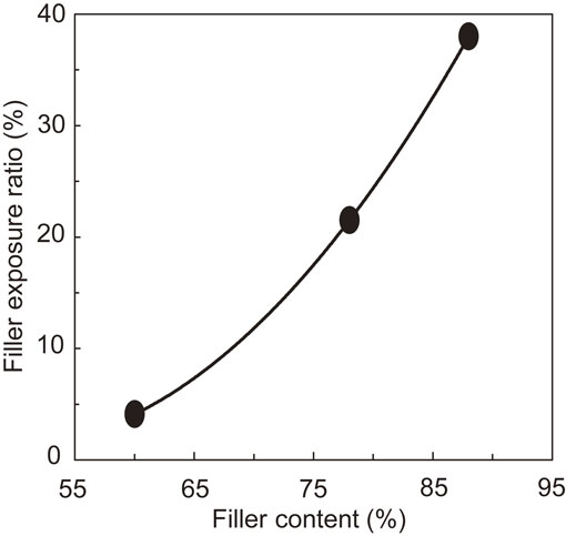
The silica filler content decreased the copper film adhesion. The relationship between the silica filler content and the silica filler exposure ratio is shown in Fig. 5. The silica filler exposure ratio as a function of the silica filler content was fitted with a quadratic function. The filler content shown on the horizontal axis of Fig. 2 was converted to the filler exposure ratio, and the results were added to the graph of Fig. 3 to produce the graph shown in Fig. 6. Decreasing the silica filler exposure ratio decreased the adhesion of the copper film. However, for the copper/stainless steel film, even if the silica filler exposure decreased to 4.1%, the peeling ratio was only 3%. Thus, we hypothesized that for the copper/stainless steel film, the stainless steel film adhered directly to the mold resin as well as to the silica filler.
4.2 Analysis of mold resin and metallic film interface
4.2.1 Depth Profile
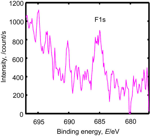
To explore the adhesion mechanism, X-ray photoelectron spectroscopy analysis of the interface was conducted on samples A–D, which were a 10 nm thick copper film, and stainless steel films formed after argon plasma etching, argon and nitrogen plasma etching, and no etching (Table 5). Samples A, B, and C and the depth profile of D are shown in Figs. 7(a)–(d). In sample A, the amount of copper decreased with depth from a depth of 2.5 nm onwards [SiO2 equivalent (the subsequent depth is also the same)]. In samples B, C, and D, the amounts of chromium and iron decreased from depths of 2.5 and 4.9 nm, respectively, and that of nickel decreased from a depth of 4.9 nm (B, C) or 2.5 nm (D). In samples A and B, the amount of nitrogen decreased from the maximum near the surface to the minimum near the interface, whereas in samples C and D the amount of nitrogen was below the minimum limit of detection. In sample D, the carbon content was higher than in the other three samples from a depth of several nanometers to 20 nm, and there was also a small amount of fluorine near the interface.

The chemical state near the interface of samples A–D was determined by narrow-scan XPS. The interface was at a depth of 7.4 nm based on the depth profile. The deconvoluted C 1s peaks are shown in Figs. 8(a)–(d) and Table 6, and the deconvoluted N 1s peaks are shown in Figs. 9(a)–(d) and Table 7.

Table 6 Deconvoluted C 1s peaks at a depth of 7.4 nm.
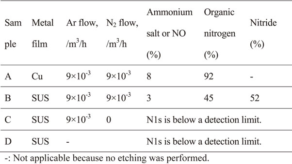
Table 7 Deconvoluted N 1s peaks at a depth of 7.4 nm.
In samples A and B, the chemical state of nitrogen indicated the presence of organic nitrogen species, such as amine, amide, and imide, although it was possible that ammonium salt or NO′′ were also present (Figs. 9(a) and (b)). In samples C and D, there were no nitrogen peaks (Figs. 9(c) and (d)). Sample D had an unetched mold resin surface, and sample C was etched with only argon; thus, the resin surface did not contain nitrogen and consisted solely of carbon, hydrogen, and oxygen from the biphenyl resin. The argon and nitrogen plasma etching performed on samples A and B produced organic nitrogen species, and the etched mold resin contained amine, amide, and imide species attributed to the effects of the nitrogen plasma. Furthermore, nitride was also observed in sample B. We hypothesized that when the mold resin was etched and carbon and nitrogen reacted on the mold resin surface, the organic nitrogen species then reacted with the iron and chromium in the stainless steel film to generate iron nitrides and chromium nitrides, which improved adhesion.
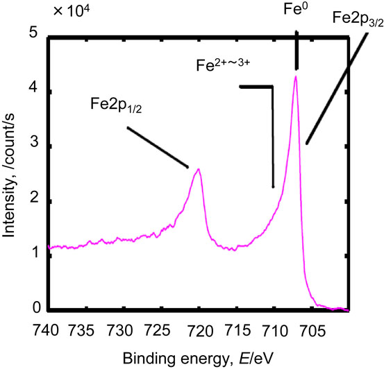
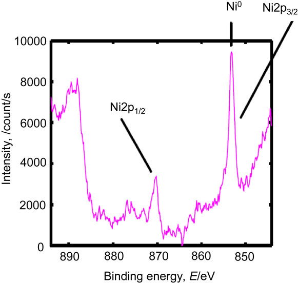
In sample A, the Cu LMM Auger peak position showed that the chemical state of the main copper species was Cu0 (metal) (Fig. 10). The chemical states of iron, chromium, and nickel in sample B are shown in Figs. 11–13. The chemical states of iron were Fe0 (metal) and Fe2+–Fe3+ (Fe2O3); those of chromium were Cr0 (metal) and Cr3+–Cr4+ (Cr2O3); and that of nickel was Ni0 (metal). Similar results were obtained for samples C and D (data not shown). The Fe2+–Fe3+ and Cr3+–Cr4+ species could have reacted with the nitrogen and carbon species on the mold resin surface to form carbides and nitrides. In sample D, a small amount of fluoride was present at the interface (Fig. 14), consistent with the depth profile. The fluoride likely originated from the mold release agent used during fabrication.
4.3 Experimental evidence for the adhesion mechanism
No carbide or nitride formation was observed in the copper film in sample A; thus, the resin probably did not react with the copper film. The adhesion of the copper film increased with the silica filler exposure, suggesting that the exposed silica filler adhered to the copper.
In sample B, carbides and nitrides formed, and carbides formed in samples C and D. For the stainless steel film, adhesion remained high even if the filler content decreased, indicating that the adhesion arose from carbides and nitrides reacting with the metal. However, adhesion failure still occurred without etching in sample D. This may be because a mold release agent containing fluorine was used in mold resin fabrication, and the residual fluoride detected on the resin surface decreased wetting with the stainless steel film, and thus also decreased film adhesion.
The adhesion remained high when the stainless steel film thickness was increased from 0.1 to 0.3 µm (Fig. 4). X-ray photoelectron spectroscopy suggested that the adhesion of the mold resin to the stainless steel film was strong because the interface was about 10 nm deep; therefore, increasing the film thickness did not affect the adhesion. This result also indicated that the adhesion mechanism for the stainless steel film to the mold resin was the formation of nitrides and carbides with the chromium and iron in the film, and that argon and nitrogen plasma etching was the key factor. Because the adhesion of the stainless steel film also increased slightly as the silica filler exposure ratio increased, the stainless steel film probably also adhered to the silica filler. Thus, for the stainless steel film, even at a low silica filler exposure ratio of 4.1%, strong adhesion was achieved via the formation of carbides and nitrides at the interface between the resin and the stainless steel film.
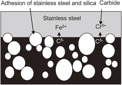
4.4 Proposed adhesion mechanism for sputtered stainless steel film with mold resin
The adhesion mechanism for the sputtered stainless steel film with mold resin was examined. The proposed adhesion mechanism for sample B with argon and nitrogen plasma etching is shown in Fig. 15. Before etching, the filler is not exposed and there is fluoride on the surface (Fig. 15(a)). The moisture in the substrate and mold resin is removed by degassing (Fig. 15(b)). The surface fluoride and resin are etched by argon and nitrogen plasma etching, exposing silica filler and, in the case of the nitrogen plasma, forming C=N bonds in the mold resin surface (Fig. 15(c)). During sputtering, the iron and chromium deposited on the resin surface bind to the nitride and carbide species, forming the interface between the resin and stainless steel film and achieving superior adhesion (Fig. 15(d)). Moreover, the stainless steel film also adheres to the exposed silica filler.
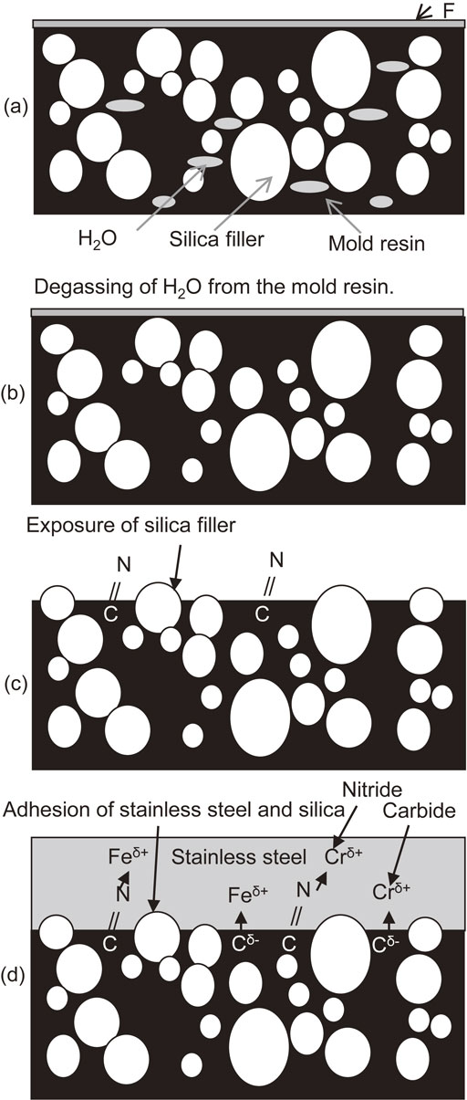
Argon plasma etching does not form nitrogen species at the resin surface, as in sample C. Therefore, only carbides react with the iron and chromium (Fig. 16), producing weaker adhesion compared with argon and nitrogen plasma etching. In sample D, because etching was not performed, the fluoride remained on the resin surface and prevented adhesion (Fig. 17).
5. Conclusion
We compared the adhesion of sputtered copper films with that of stainless steel and copper/stainless steel films to a mold resin substrate for various silica filler contents. We also examined the effect of etching the resin surface on the resin-film interface, and the relationship with the film adhesion. The factors that affected film adhesion were revealed and the adhesion mechanism of the stainless steel film to the resin was clarified. The results were as follows.
-
(1)
For the copper film, when the filler content was reduced to 60%, adhesion decreased, and the peeling ratio was 100%. However, for the copper/stainless steel film, the peeling ratio was 0% at filler content of 88% and 78%. For a filler content of 60%, the peeling ratio increased only slightly to 3%.
-
(2)
For the copper film, when the silica filler exposure ratio was less than 4.4%, the peeling ratio was 100%, whereas for the copper/stainless steel film at a silica filler exposure ratio of 4.1%, the peeling ratio was only 3%. At a filler exposure ratio of 0% (no etching), the peeling ratio was 100% for both the copper and copper/stainless steel films.
-
(3)
X-ray photoelectron spectroscopy showed that for the copper film, the main species at the interface were CHx, C–C, and C=C, and that organic nitrogen species were detected. For the stainless steel film, after argon and nitrogen plasma etching, carbides and nitrides were detected, whereas after argon plasma etching only carbides were detected. Adhesion of the stainless steel film to the resin arose from the formation of carbides and nitrides. Without etching, fluoride was detected at the interface, which explained the adhesion failure.
-
(4)
The following mechanism for the adhesion between the sputtered stainless steel and the mold resin and film formation was proposed based on the experimental results. Moisture was removed from the substrate and mold resin by degassing. The fluoride on the mold resin surface and the resin were etched, exposing the silica filler, which then could adhere to the stainless steel film. Carbides and nitrides were formed by the argon and nitrogen plasma etching on the resin surface. The strong adhesion arose from the reaction of the carbides and nitrides with the iron and chromium in the stainless steel film. Because the adhesion remained strong even at a silica filler exposure ratio of 4.1% for the stainless steel film, the main adhesion mechanism was thought to be carbide and nitride formation.
Acknowledgments
The authors would like to thank Mr. Kiyokazu Okada, Mr. Hiroaki Hazama, and Mr. Chiaki Takubo (Kioxia Corporation) for excellent advice and useful information. This research did not receive any specific grant from funding agencies in the public, commercial, or not-for-profit sectors.
REFERENCES
- 1) T. Sudo, H. Sasaki, N. Masuda and J.L. Drewniak: IEEE Trans. Adv. Packag. 27 (2004) 304–314. doi:10.1109/TADVP.2004.828817
- 2) A.B. Aripin, M. Nishi, K. Suzuki and K. Hayakawa: Mater. Trans. 61 (2020) 251–255. doi:10.2320/matertrans.MT-ML2019008
- 3) F.R.I. Gomez and R.S. Rodriguez: IJSES 3(8) (2019) 12–13. doi:10.5281/zenodo.3407963
- 4) W. Guo, Z. Zeng, X. Zhang, P. Peng and S. Tang: J. Nanomater. 2015 (2015) 897142. doi:10.1155/2015/897142
- 5) H.-C. Cheng, C.-R. Chen, S.-H. Hsu and K.-B. Cheng: Sustainability 12 (2020) 5899. doi:10.3390/su12155899
- 6) K. Joo, T.-R. Kim, J.W. Hwang, J.-H. Yoon, S.Y. Jeong and M.J. Yim: 2017 IEEE 67th Electron. Compon. Technol. Conf., (Institute of Electrical and Electronics Engineers, 2017) pp. 1736–1741.
- 7) T.M. Fee, L.S. Kah, G.S. Lock, K.S. Leong, K. Mukai and T. Magaya: 2014 IEEE Int. Conf. Semiconduct. Electron., (Institute of Electrical and Electronics Engineersm 2014) pp. 313–316.
- 8) M.F. Tai, S.L. Kok, K. Mukai, S. Hotz, P. Brooks and D.R. Cocina: Adv. Sci. Technol. Eng. Syst. J. 2 (2017) 1159–1164. doi:10.25046/aj0203146
- 9) Y. Lu, Q. Liang and L. Xue: Surf. Coat. Tech. 206 (2012) 3639–3644. doi:10.1016/j.surfcoat.2012.02.059
- 10) D. Schaubroeck, L. Mader, P. Dubruel and J. Vanfleteren: Appl. Surf. Sci. 353 (2015) 238–244. doi:10.1016/j.apsusc.2015.06.114
- 11) Y. Lu, S. Jiang and Y. Huang: Surf. Coat. Tech. 204 (2010) 2829–2833. doi:10.1016/j.surfcoat.2010.02.061
- 12) S.X. Jiang and R.H. Guo: Surf. Coat. Tech. 205 (2011) 4274–4279. doi:10.1016/j.surfcoat.2011.03.033
- 13) T. Yamazaki, Y. Takano and S. Honma: Toshiba Rev. 71 (2016) 16–19.
- 14) Y.-S. Choi, Y.-H. Yoo, J.-G. Kim and S.-H. Kim: Surf. Coat. Tech. 201 (2006) 3775–3782. doi:10.1016/j.surfcoat.2006.03.040
- 15) A.A. Taylor, M.J. Cordill, L. Bowles, J. Schalko and G. Dehm: Thin Solid Films 531 (2013) 354–361. doi:10.1016/j.tsf.2013.01.016
- 16) N. Marin and Y. Serruys: Nucl. Instrum. Methods Phys. Res. B 105 (1995) 175–180. doi:10.1016/0168-583X(95)00551-X
- 17) Y. Takagi, Y. Gunjo, H. Toyoda and H. Sugai: Vacuum 83 (2008) 501–505. doi:10.1016/j.vacuum.2008.04.049
- 18) S.H. Kim, S.W. Na, N.-E. Lee, Y.W. Nam and Y.-H. Kim: Surf. Coat. Tech. 200 (2005) 2072–2079. doi:10.1016/j.surfcoat.2005.05.021
- 19) S.H. Kim, S.H. Cho, N.-E. Lee, H.M. Kim, Y.W. Nam and Y.-H. Kim: Surf. Coat. Tech. 193 (2005) 101–106. doi:10.1016/j.surfcoat.2004.08.130
- 20) K. Miyauchi and M. Yuasa: Prog. Org. Coat. 76 (2013) 1536–1542. doi:10.1016/j.porgcoat.2013.06.009
- 21) T. Miyamura and J. Koike: Mater. Sci. Eng. A 445–446 (2007) 620–624. doi:10.1016/j.msea.2006.09.097
- 22) S. Iwamori, T. Miyashita, S. Fukuda, N. Fukuda and K. Sudoh: J. Vac. Soc. Jpn. 39 (1996) 103–110. doi:10.3131/jvsj.39.103
- 23) S. Iwamori, T. Miyashita, S. Fukuda, N. Fukuda and K. Sudoh: J. Vac. Soc. Jpn. 39 (1996) 295–301. doi:10.3131/jvsj.39.295
- 24) T. Miyashita, S. Iwamori, S. Fukuda, N. Fukuda and K. Sudoh: J. Vac. Soc. Jpn. 39 (1996) 11–14. doi:10.3131/jvsj.39.11
- 25) C. Yang, S. Lee, J. Wu and T. Lin: Appl. Surf. Sci. 252 (2005) 1818–1825. doi:10.1016/j.apsusc.2005.03.182
- 26) J.S. Eom and S.H. Kim: Thin Solid Films 516 (2008) 4530–4534. doi:10.1016/j.tsf.2008.01.022
- 27) B. Noh, J. Yoon, J. Choi and S. Jung: Mater. Trans. 51 (2010) 85–89. doi:10.2320/matertrans.M2009276
- 28) J.Y. Song and J. Yu: Acta Mater. 50 (2002) 3985–3994. doi:10.1016/S1359-6454(02)00197-0
- 29) Y. Oh, E.J. Kim, Y. Kim, K. Choi, W.B. Han, H.-S. Kim and C.S. Yoon: Thin Solid Films 600 (2016) 90–97. doi:10.1016/j.tsf.2016.01.010
- 30) J. Ge, M.P.K. Turunen and J.K. Kivilahti: Thin Solid Films 440 (2003) 198–207. doi:10.1016/S0040-6090(03)00851-4
- 31) ASTM D3359-97 (ASTM International, 1997).