Abstract
Bonding copper in the solid state requires either a high temperature, large deformation, or high vacuum. In the present study, copper was butt-bonded using a K-shaped groove at 298 K under no bonding pressure through copper electrodeposition. The initial gap between the faying surfaces of the copper rods were gradually filled with the electrodeposition of copper from the center to the periphery. No significant defects were observed in the bond layer, and a high joint strength of approximately 240 MPa was obtained. There were three regions in the bond layer: fine columnar grain region, ultrafine grain region, and recrystallized grain region. The size of the ultrafine grains was several tens of nanometers, and the microhardness was larger than that of the base metal. As electrodeposition progressed, there were insufficient additives for electrodeposition near the center of the bond layer, and recrystallization occurred owing to self-annealing.
1. Introduction
The miniaturization of electronic devices implies an increase in the number of junctions and a downsize of the junctions. The increase in the number of chip components in a device requires a low-temperature and low-load process for joining and packaging. Although the joining material responsible for the electrical connection is generally soldered, copper and its alloys with a low electrical resistivity and high melting point are advantageous considering the electrical loss at the joint and the usage at high temperature. In general, diffusion bonding, ultrasonic bonding, and friction stir welding are applied to bond copper and its alloys in the solid state. However, at a bonding temperature of approximately 1000 K, a bond time of several tens of minutes and a bonding pressure of several MPa are required, and the diffusion bonding process must be conducted under a high-vacuum atmosphere at 10−3 Pa to obtain sound copper-to-copper joints.1,2) Although ultrasonic bonding can be performed in air and at room temperature, it requires high bonding pressures and involves a significant deformation of the copper in the bond.3,4) Friction stir welding can also be performed in air, but the temperature of the joint will be high, resulting in significant deformation.5,6) In addition, any aforementioned joining method requires a tool to be pressed against the joint to apply pressure and is not suitable for joining narrow gaps where the tool cannot access. Therefore, the authors have reported similar copper bonding using electrical plating technology that can be performed at low temperature without bonding pressure.7)
In electronic devices, plating technology is used as a surface modification technique, such as tin plating and gold plating, to improve the wettability between electrodes and solders, and Ni or Ni–P plating is used as a diffusion barrier for elements.8,9) There are few studies on the joining process using plating technology. For example, Kato et al. used electrodeposited Ni around copper nanoparticles to bond a chip to an electrode as a die bond for power devices.10) Yang et al. reported dissimilar material bonding between copper and aluminum by nickel deposition.11) Zhang et al. reported the multipoint simultaneous bonding of nickel nanowires by silver electrodeposition.12) The problem with joining by electrodeposition is that as electrodeposition proceeds, the gap between the bonded surfaces becomes smaller, and the bath containing the metal ions necessary for electrodeposition decreases. Therefore, the authors reported that copper can be bonded by electrodeposition using an electrolytic bath containing several organic additives,7) referring to the bath composition used in the damascene process,13–15) that fills microvias on a substrate with copper. The copper-to-copper butt joint was achieved by electrodeposition of copper between copper bars (I-shaped groove) facing each other with a gap of 100 µm in the electrolytic bath. However, electrodeposition tended to occur preferentially near the outer periphery, where the current density and copper ion concentration could be high, resulting in a joint with certain unbonded areas remaining near the center of the faying surface.
In this study, copper was bonded to copper through copper electrodeposition using a joint preparation with a K-shaped groove to control the direction of copper deposition from the center to the periphery of the joint. The microstructure of the bond layer and the mechanical properties of the joint were evaluated.
2. Experimental Procedures
The materials used were oxygen-free copper rods of 1 mm and 5 mm in diameter and an oxygen-free copper plate. The faying surface of a copper rod with a diameter of 1 mm was conically machined with an extruded length of 0.1 mm. The faying surfaces were degreased with acetone and acidified with 5% sulfuric acid. Then, soft etching was performed for 30 s in a solution of 0.72 mol/L sulfuric acid and 1 mol/L hydrogen peroxide to improve the adhesion of the electrodeposits to copper. Table 1 lists the compositions of the electrodeposition baths. Bath-B is a basic bath for copper electrodeposition containing CuSO4, H2SO4, and HCl. Bath-A comprises Bath-B with three types of organic additives: polyethylene glycol (PEG), Bis-(sodium sulfopropyl)-disulfide (SPS), and Janus Green B (JGB). Baths-C, D, and E comprise Bath-B with one additive each.

Table 1 Compositions of electrodeposition baths.
The bonding of copper was performed in Bath-A. Copper electrodeposition was performed on the copper plate in Baths-A, B, C, D, and E to investigate the effect of additives on the microstructure of the electrodeposition. Figure 1 shows a schematic of the bonding setup. A copper rod with a flat faying surface and a copper rod with a conical faying surface were attached to each other to form a butt joint. In the following, this joint preparation is described as a K-shaped groove. A region of 4 mm from the faying surfaces was left, and the rest of the rod surfaces were coated with resin to restrict the current. Both copper rods were immersed in Bath-A in a state where they were attached to each other and used as cathode electrodes. An oxygen-free copper was used as the anode electrode that was energized using a DC power supply. The current density was 20 mA/cm2, the temperature of the electrodeposition bath was 298 K, and the deposition time, that is, the bond time, was varied from 10.8 to 18.0 ks. The bath was stirred using a stirrer. To investigate the effect of bath stirring, two cases were considered; in the first case, the bath was left unstirred, and in the second case, it was strongly stirred.

The cross-sections of the joints and the electrodeposited layer on the copper plate were polished with emery paper and then finished with diamond and OP-U colloidal silica slurry. After polishing, the cross-sections of the specimens were chemically etched with a mixed solution of sodium dichromate and sulfuric acid and observed using an optical microscope. The details of the microstructure of the electrodeposited layer were also observed by field-emission scanning electron microscopy (FE-SEM) with electron backscatter diffraction analysis (EBSD) and transmission electron microscopy (TEM) with energy dispersive X-ray spectroscopy (EDS). The microhardness (HT115) of the joint was evaluated using a dynamic ultra-microhardness tester (Shimadzu Co., Ltd., DUH-211) equipped with a 115° triangular pyramid indenter. The joint strength was evaluated using a shear test. The crosshead speed was set to 0.025 mm/s.
3. Results
3.1 Microstructures of the bond layer
The authors reported that when copper was electrodeposited on a copper plate at 298 K in Bath-A with stirring, the growth rate remained constant even when the process was performed at 20 mA/cm2 for 18.0 ks, that is, there was no shortage of ions or additives under these conditions.7) Figure 2 shows the cross section of the optical microscopic image and inverse pole figure (IPF) maps of the copper electrodeposition layer on the copper plate under a current density of 20 mA/cm2 for 18.0 ks at 298 K in Bath-A without stirring. No delamination was observed at the interface. The base plate was chemically etched well, and grains of several tens of micrometers in size were observed. In contrast, optical microscopy did not reveal any microstructures in the deposition layer even after chemical etching. The IPF maps revealed that the electrodeposition layer comprised a homogeneous microstructure from the interface to the surface that was composed of ultrafine grains of several hundred nanometers in size.
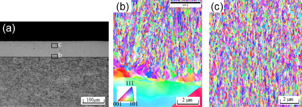
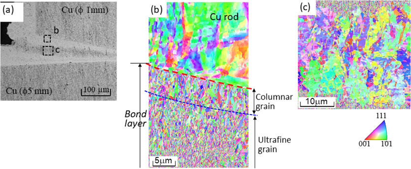
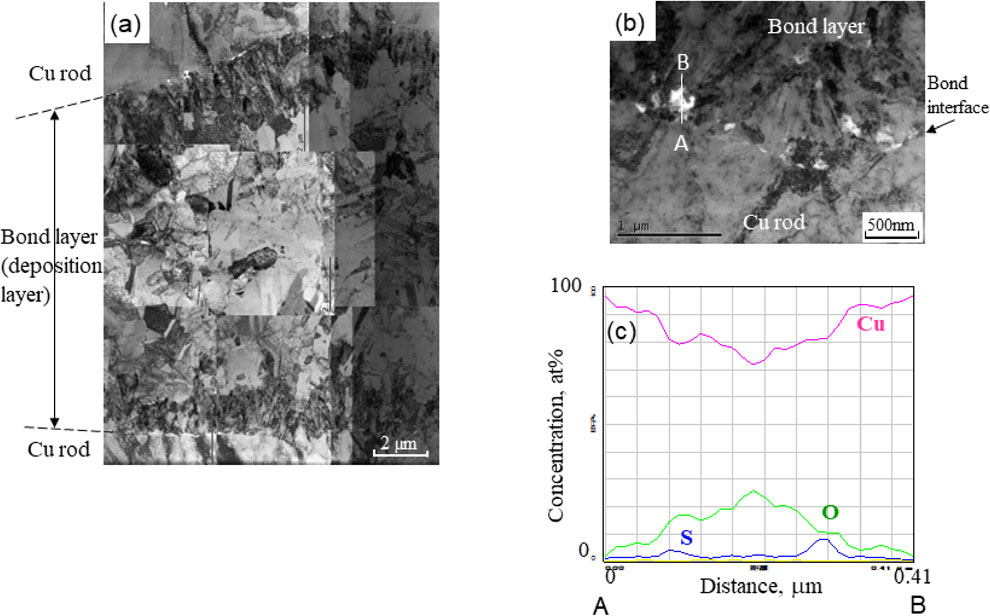
Figure 3 shows the cross sections of the copper-to-copper joints by copper electrodeposition for different bond times. At a bond time of 10.8 ks, the joint gap near the initial contact point in the center of the faying surface began to be filled with deposited copper. As the bond time increased, the initial gap between the faying surfaces was filled with deposition. When the bond time reached 18.0 ks, the gap was completely filled with copper deposition. No significant defects were observed in the bond layer by optical microscopy. However, unlike the uniform microstructure shown in Fig. 2, the bond layer which is the electrodeposition consisted of bright and slightly darker etched regions. Next, the bond layer was observed using FE-SEM with EBSD analysis. Figure 4 depicts the inverse pole figure (IPF) maps of the bond layer with a bond time of 18.0 ks. The fine columnar grains grew from the faying surface to a thickness of 5–10 µm. An ultrafine grain structure with a grain size of several hundred nanometers was grown following the columnar grain region. These two fine grain regions correspond to the bright region of electrodeposition in the optical microscope image shown in Fig. 4(a). Slightly coarse grains including twins were observed in the center of the bond layer, which corresponds to the dark region of electrodeposition in the optical microscope image. Because the grain size was larger than that in the other regions and twins were observed, the grains were coarsened owing to recrystallization at room temperature; this is called self-annealing. TEM bright-field images of the bond layer are depicted in Fig. 5. The electrodeposited copper grew from the facing faying surfaces and was bonded. No obvious bond interfaces or significant defects were observed in the bond layer. However, certain inclusions remained at the interface between the base metal and the electrodeposited copper. EDS analysis revealed that they were metallic oxides.
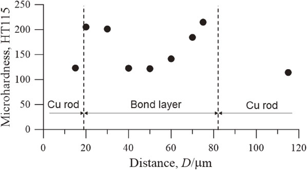
The microhardness (HT115) of the bond layer is shown in Fig. 6. The microhardness was measured on a line running longitudinally between the copper rods across the bonding layer. The microhardness of the copper rod was approximately 120. The microhardness in the ultrafine region in the bond layer was approximately 210 that was larger than that of the base metal owing to grain refinement. The microhardness at the center of the bond layer was smaller than that in the ultrafine region in the bond layer because of the recrystallized region, as shown in Fig. 4(c). The shear strength of the joints is shown in Fig. 7. The joint strength was extremely low at the bond time of 10.8 ks because only the area near the center of the K-shaped groove was filled with electrodeposited copper, as shown in Fig. 3(a). As the bond time increased, the groove was gradually filled with the electrodeposited copper, resulting in an increase in the joint strength. When the bond time was 18.0 ks, the K-shaped groove was filled entirely with electrodeposited copper, and the joint strength reached approximately 240 MPa. Because the joint strength was evaluated using a shear test, all joints were fractured at the bond interface. The typical fracture surfaces are depicted in Fig. 8. The main fracture path was at the interface between the electrodeposited copper and the base metal and partially through the electrodeposited copper. The fracture surface of electrodeposited copper exhibited a dimple morphology, indicating that it had sound ductility properties. However, as shown in Fig. 5, the oxides remained at the interface between the base metal and the electrodeposited copper, and the fracture passed mainly through the interface. To improve the bonding strength, surface pretreatment before electrodeposition must be improved in the future.
4. Discussion
In the present study, an electrodeposition bath used in the filling process for microvias was used to fill the initial joint gap of the K-shaped groove with electrodeposited copper.14) Bath-A is composed of a basic copper sulfate bath for general copper electrodeposition with the addition of PEG, SPS, and JGB (Table 1). Although the initial gap in the joint with the I-shaped groove was not completely filled with copper,7) the gap was completely filled with electrodeposited copper in the K-shaped groove, and sound joints were obtained (see Fig. 3(c)). However, the microstructure of the bond layer was inhomogeneous, comprising an ultrafine grain region and a recrystallized region (see Fig. 4). It is well known that electrodeposited copper is recrystallized easily even at room temperature, that is, self-annealing.16,17) Thus, it has been reported that self-annealing can be suppressed by adding compounds such as sodium 2-Mercapto-1H-benzimidazole-5-sulfonate dihydrate (2M-5S).18) The change in bath composition during the growth process of electrodeposition might be one reason for the formation of an inhomogeneous microstructure in the bond layer. As shown in Fig. 2, copper electrodeposition comprising ultrafine grains was obtained on a copper plate using Bath-A. This implied that the composition of the bath near the bonding surface might have changed during the bonding process. Electrodeposition was then performed on a copper plate using a basic copper sulfate bath (Bath-B) with one each of PEG, SPS, and JGB contained in Bath-A used for bonding. Figure 9 shows the cross-sectional micrographs of the electrodeposited layer on the copper plate using Baths-B, -C, -D, and -E. The baths were not stirred. Electrodeposition using Bath-B, which contained no additives, showed large surface irregularities and very coarse microstructures. Electrodeposition using Baths-C and -D, in which PEG or SPS was added to Bath-B, had less surface irregularity and a slightly finer microstructure than electrodeposition in Bath B. When electrodeposition was performed in Bath-E, in which JGB was added to Bath-B, copper electrodeposits were only partially formed, but not as plating. Although the microstructure was slightly refined by the addition of PEG and SPS, finer microstructures, such as the submicron-sized grains, were observed in the bonded layer. These results suggested that the microstructure of the electrodeposition was coarsened owing to the lack of additives in Bath-A. During electrodeposition, copper ions and additives in the bath were supplied to the substrate surface by diffusion, and copper was deposited by receiving electrons from the substrate as the cathode. If the bath was not sufficiently stirred, the diffusion layer would become thick, and depending on the conditions, the supply of additives would be insufficient for the supply of electrons.

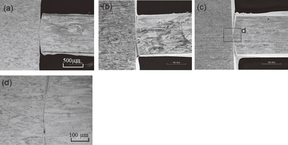
Because Bath-A was stirred during the bonding process, sufficient ions and additives were present even at the center of the K-shaped groove at the initial stage of the deposition. Therefore, the initial deposition near the faying surface exhibited an ultrafine microstructure. However, as the bonding progressed, that is, as electrodeposition proceeded, the gap became narrower, and the effect of stirring the bath in the gap might be less if the bath was only stirred from outside the joining gap. In this case, the supply of the additive to the bonding surface was dominated by diffusion in the liquid. Therefore, the additive was insufficient in the final bonding area, resulting in microstructure coarsening owing to self-annealing. To investigate the stirring effect, bonding was performed in a strongly stirred bath and an unstirred bath. Figure 10 shows the cross sections of the joints bonded in the strongly stirred bath and in the non-stirred bath. The rotation speed of the stirrer was approximately 1.5 times faster than that of normal bonding. In the unstirred state, a recrystallized region was formed in the center of the bond layer, as in the joint bonded under normal stirring conditions, as shown in Fig. 3(c). Although the recrystallization region was also formed in the center of the bond layer, even under strong stirring conditions, its width was reduced. This indicates that it is necessary to stabilize the bath composition even at the end of the bonding process to reduce softening owing to self-annealing in the center of the bond layer. To improve the insufficient supply of additives at the end of the bonding process, it will be necessary to reduce the electrodeposition rate or optimize the groove shape in the future. In some cases, a few pores were observed in the center of the bond layer regardless of the stirring conditions (see Fig. 10(c)). Since the growth rate of electrodeposition in a narrow gap cannot be completely controlled, electrodeposition may proceed leaving such pores. The formation of residual pores may also be due to the change in bath composition in the narrow gap during the electrodeposition.

5. Conclusions
The oxygen-free copper was bonded through the electrodeposition process, and the microstructural development of the bond layer and the joint strength were investigated. The main results are as follows.
-
(1)
When copper was electrolytically deposited in a bath containing three different additives when a copper rod with a conically machined tip and a flat copper bar were butt-joined, copper was deposited from the initial contact point in the center of the faying surface, gradually filling the initial bonding gap completely as the bond time increased. Finally, the copper rods bonded with one another with a bond time of 18.0 ks under a current density of 20 mA/cm2 at 298 K under no pressure.
-
(2)
No significant defects were observed in the bond layer. A shear joint strength of approximately 240 MPa was obtained. Because the fragmented oxides remained at the interface between the base copper and the electrodeposited copper, the fracture path was mainly at the interface and partially propagated through the electrodeposited copper.
-
(3)
The bond layer consisted of three regions: a fine columnar crystalline region, an ultrafine grain region with a grain size of several hundred nanometer, and a recrystallized region, in order from the faying surface. The microhardness in the ultrafine grain regions was higher than that of the base metal owing to grain refinement. The recrystallization region at the center of the bond layer was softer than that of the other regions in the bond layer.
-
(4)
The area near the center of the bond, which is the final deposition area, might have been recrystallized at room temperature owing to an insufficient supply of additives. By increasing the stirring intensity, the self-annealing region in the bonding layer was reduced.
REFERENCES
- 1) B. Derby and E.R. Wallach: J. Mater. Sci. 19 (1984) 3140–3148. doi:10.1007/BF00549797
- 2) K.-C. Shie, A.M. Gusak, K.N. Tu and C. Chen: J. Mater. Res. Technol. 15 (2021) 2332–2344. doi:10.1016/j.jmrt.2021.09.071
- 3) Y. Arai, M. Nimura and H. Tomokage: Trans. Japan Inst. Electron. Packag. 7 (2014) 8–13. doi:10.5104/jiepeng.7.8
- 4) Y. Tian, C. Wang and Y.N. Zhou: Trans. Nonferrous Met. Soc. China 18 (2008) 132–137. doi:10.1016/S1003-6326(08)60024-2
- 5) Y.F. Sun and H. Fujii: Mater. Sci. Eng. A 527 (2010) 6879–6886. doi:10.1016/j.msea.2010.07.030
- 6) P. Nagabharam, D. Srikanth Rao, J. Manoj Kumar and N. Gopikrishna: Mater. Today Proc. 5 (2018) 1264–1270. doi:10.1016/j.matpr.2017.11.210
- 7) K. Nakamura, M. Matsushima and S. Fukumoto: Proc. the 27th Symposium on Microjoining and Assembly Technology in Electronics, 27, (2021) pp. 257–261 (in Japanese).
- 8) T.Y. Lin, C.N. Liao and A.T. Wu: J. Electron. Mater. 41 (2012) 153–158. doi:10.1007/s11664-011-1740-8
- 9) N.B. Duong, T. Ariga, L.B. Hussain and A.B. Ismail: Mater. Trans. 49 (2008) 1462–1466. doi:10.2320/matertrans.MRA2007209
- 10) N. Kato, S. Hashimoto, T. Iizuka and K. Tatsumi: Trans. Japan Inst. Electron. Packag. 6 (2013) 87–92. doi:10.5104/jiepeng.6.87
- 11) Y. Yang, H. Chen and M. Li: J. Mater. Process. Technol. 242 (2017) 68–76. doi:10.1016/j.jmatprotec.2016.11.025
- 12) H. Zhang, S. Wang, C. Hang and Y. Tian: Weld. World 65 (2021) 1021–1030. doi:10.1007/s40194-021-01066-7
- 13) P. Vereecken, R. Binstead, H. Deligianni and P.C. Andricacos: IBM J. Res. Dev. 49 (2005) 3–18. doi:10.1147/rd.491.0003
- 14) W.-P. Dow, M.-Y. Yen, S.-Z. Liao, Y.-D. Chiu and H.-C. Huang: Electrochim. Acta 53 (2008) 8228–8237. doi:10.1016/j.electacta.2008.06.042
- 15) J.B. Marro, C.A. Okoro, Y.S. Obeng and K.C. Richardson: J. Electrochem. Soc. 164 (2017) D543–D550. doi:10.1149/2.1131707jes
- 16) S. Lagrange, S.H. Brongersma, M. Judelewicz, A. Saerens, I. Vervoort, E. Richard, R. Palmans and K. Maex: Microelectron. Eng. 50 (2000) 449–457. doi:10.1016/S0167-9317(99)00314-7
- 17) M. Stangl, J. Acker, V. Dittel, W. Gruner, V. Hoffmann and K. Wetzig: Microelectron. Eng. 82 (2005) 189–195. doi:10.1016/j.mee.2005.07.059
- 18) M. Matsuda, S. Yoshihara and M. Dobashi: J. Surf. Finish. Soc. Jpn. 59 (2008) 696–700 (in Japanese). doi:10.4139/sfj.59.696