Abstract
Demand for lead-free, free-cutting brass is increasing in response to lead regulations in Europe. The authors of this paper have attempted to develop a lead-free brass with an α + β two-phase microstructure, which is different from existing C6932 alloy. As a result of basic investigations, it was found that the addition of Si to β-brass dramatically reduces the cutting resistance due to an effect that appears to be a reduction in the stacking defect fault energy, and that if phosphorus compounds are dispersed in such β-brass, the compounds make stress concentration sources improving chip fragmentation during cutting. Based on these findings, we have succeeded in developing a new free-cutting α + β brass (62.5Cu–1Si–0.07P–Zn). The developed alloy contains about 55% alpha phase and has excellent machinability and 1.3 times higher strength than C3604.
This Paper was Originally Published in Japanese in J. Japan Inst. Copper 61 (2022) 323–328.
1. Introduction
In Europe, the RoHS Directive, which regulates the amount of lead in materials used in electrical and electronic products to be 0.1% or less, has been enforced since 2006, and the ELV Directive, which is linked to the RoHS Directive, has also been enforced for automotive parts. However, lead contained in free-cutting copper alloys (hereinafter referred to as “lead brass”) has been exempted from both directives due to the lack of alternative materials, and up to 4% lead has been permitted in effect. This exemption is a time-limited measure, though, and each time a deadline is reached, whether or not to abolish the exemption is discussed, and various evaluations and studies are conducted by technical consultants. Demand for lead-free free-cutting brass is steadily increasing in anticipation of the possibility of the removal of the exemption in the near future.
In the review of the exemptions, various industries and technical consultants have reported on the possibility of substituting lead brass with lead-free free-cutting brass. Particularly, in the 2016 RoHS and ELV final reports,1,2) there is a notable description regarding ECO BRASS3) (JIS C6932, EN CW724R, ASTM C69300, 76Cu–3Si–0.1P–Zn, hereinafter “C6932”). In summary, it states that the constraints on the use of C6932 may be overcome in the next few years. C6932 is the only alloy that has been publicly presented as having a realistic possibility as a lead brass substitute. C6932 is already well recognized in the market with a cumulative production volume of over 300,000 tons in Japan, the U.S., and Europe as of 2019. However, there are more than 10 types of lead brass alloys registered in the JIS standard, and it is unrealistic to expect that C6932 alone can replace all of them. Although the future direction of lead regulations is unclear, there is no doubt that hazardous substances that place a heavy burden on people and the environment will be eliminated, and it is hoped that new types of lead-free copper alloys will emerge. Under these circumstances, the authors have tackled with the development of a new lead-free free-cutting brass and succeeded in completing it. This paper mainly reports the results of basic research on the machinability of the β phase and the properties of the developed alloy.
2. Design Concept of the New Alloy
C6932 has excellent machinability due to its characteristic 3-phase microstructure of α (fcc) + κ (hcp) + γ (bcc).3) At the same time, it has high strength, excellent wear resistance, dezincification corrosion resistance, and stress corrosion cracking resistance. Therefore, it can be said that C6932 has different properties from those of C3604, a typical lead brass containing 3 mass% Pb. For this reason, the new alloy was developed aiming for having α (fcc) + β (bcc) two-phase microstructure like C3604. An α + β brass has advantages over other copper alloys in terms of economy, hot workability, and strength. In general, the β phase of an α + β brass is said to have better machinability than the α phase, but there are many unknowns about the properties of the β phase. Therefore, we focused on the β phase, for which there was still ample room for research, and proceeded from a basic investigation of the machinability of the β phase.
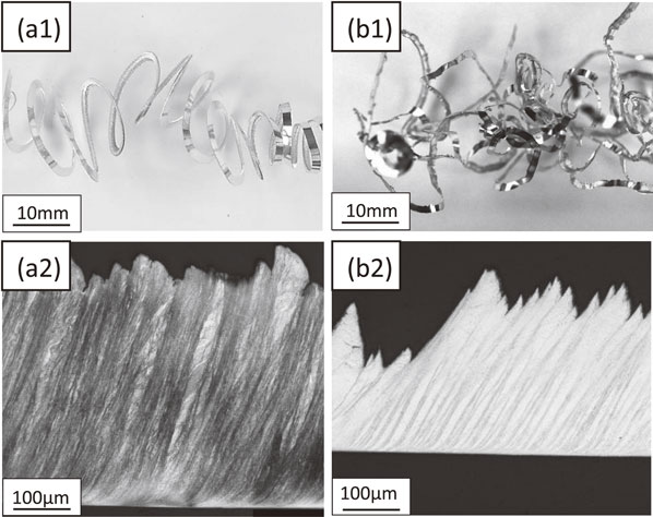
First, as a preliminary experiment, 65Cu–35Zn α single-phase brass (hereinafter α-brass) and 54Cu–46Zn β single-phase brass (hereinafter β-brass) were turned with a lathe, then cutting resistance was measured and chips were collected. The appearance and cross-sectional microstructure of the chips are shown in Fig. 1. The appearance and cross-sectional microstructure of the α-brass chips have typical characteristics of flow-type chips. On the other hand, chips of β-brass are entangled that is troublesome to handle. However, the cutting resistance was about 25% lower than that of the α-brass. Observing the cross-section of the β-brass chips, it was learned that thin and thick chips coexisted. It is presumed that the large variation in thickness is causing the entanglement. However, the free surface (reverse surface of the machined surface of a chip) has rectilinear fractures, suggesting that β-brass may have good machinability even though the free surface is uneven.
To improve and enhance the machinability of β-brass, we decided to add Si. Figure 2 shows how the stacking fault energy4) changes when the contents of Zn and Si added to Cu are changed. Valence electron density represented by the x-axis in Fig. 2 is defined by e/a = 1 + (Z − 1) C in which “Z” represents the valence of an element added (which is 4 if the element is Si, and 2 if Zn is added) and “C” represents the concentration of the element. This figure indicates that the higher the amount of Zn, the lower the stacking fault energy of brass compared with that of pure copper, but it should be noted that the stacking fault energy of Cu–Si alloy is lower than that of brass. Therefore, it was expected that an addition of Si to brass would further lower the stacking fault energy. There was a hope that the stacking faults would act as an obstacle to dislocation migration and promote work hardening, resulting in stable generation of shear type chips during cutting. The above hope is regarding α-brass, but the authors predicted that the same would apply to β-brass as well.

On the other hand, to further promote chip fragmentation, it is considered effective to disperse fine and hard precipitates, which may act as a source of stress concentration during cutting in the microstructure. Simultaneously, various elements were explored as candidates to add to a β-brass. As a result, we came to conclude that phosphorous compounds would be the most promising.
3. Experimental Methods
In the laboratory, a β-brass containing 54 mass% Cu and 46 mass% Zn was used as base alloy, and the contents of Cu and Zn were adjusted to maintain a β single-phase state. Alloys to which 0–1.4 mass% Si was added to the base β-brass and those to which 0.07 mass% P were further added were prepared by melting. They were cast to form a rod of 95 mm in diameter, hot extruded to a diameter of 24 mm with a 500-ton laboratory extruder, then heat-treated at 500°C for 2 hours to make sure the microstructure would consist of 100% β phase, and air-cooled. A commercially available C3604 rod of 25 mm in diameter was used as comparative material.
In the case of the developed alloy, a billet of 240 mm in diameter which was cast with a casting machine normally used for the manufacture of commercial products was hot extruded to 25.6 mm in diameter with a 3,000-ton direct extruder and finished by drawing to 25 mm in diameter. To examine the mechanical properties, another billet was prepared by hot extruding with a 2750-ton indirect extruder and drawing to specific dimensions.
Cutting tests were conducted on each sample using a lathe and a drilling machine. The conditions for the test lathing were as follows - cutting speed: 40 m/min, feed rate: 0.11 mm/rev, and depth of cut: 1 mm. The tool used was a K10 carbide turning tool (nose diameter: 0.4 mm). The cutting resistance was determined by the principal force. On the other hand, the conditions for the drilling were as follows: cutting speed: 12.6 m/min and feed rate: 0.11 mm/rev. The drill used was a high-speed steel straight drill (φ3.5 mm).
The appearance and cross section of the chips collected in each test were observed. The cross sections of the chips were embedded in resin perpendicular to the direction in which the chips were generated, polished, and observed.
4. Experimental Results and Discussion
4.1 Effects of Si and P on machinability of β-brass
Figure 3 shows the relationship between the amount of Si added to a β-brass and the cutting resistance when turning with a lathe, and also the relationship between the amount of Si added to a β-brass containing 0.07 mass% P and the cutting resistance, which indicates the effect of Si on the machinability of β-brass. Figure 4 and Fig. 5 show typical appearance and cross section of the chips obtained during the test turning and the test drilling, respectively, along with those of C3604.
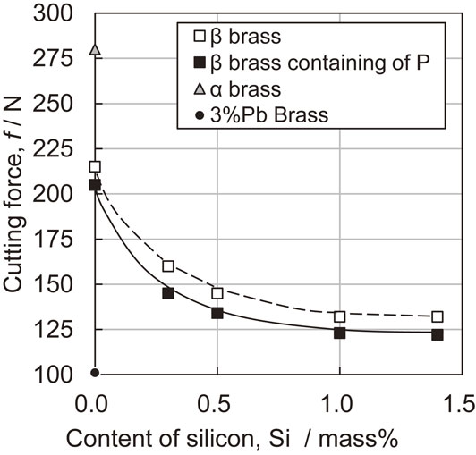

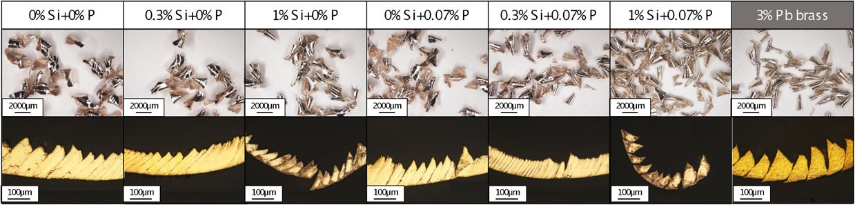
Figure 3 shows that the cutting resistance of β-brass decreases about 25% when only 0.3 mass% Si is added. The cutting resistance continues to decrease as the Si content is increased. When the Si content is 1 mass%, the cutting resistance decreases about 40%. The pictures of cross section in Fig. 4 show that when 0.3 mass% Si is contained, the chip is thin and its thickness is quite stable. Also, rectilinear fractures are clearly formed on the free surface. When 1 mass% Si is contained, thickness is even. When the concentration of Si reaches this point, the chips finally begin to break up spontaneously, but that is still not enough. The reason that thin and so-called shear type chips are generated when a small amount of Si is contained in β phase is presumed to be the further reduction in stacking fault energy shown in Fig. 2, which not only applies to the α phase but also applies to the β phase even though its crystal structure is different from that of the α phase.
Figure 6 shows the microstructure of a sample of β-brass containing 1 mass% Si and 0.07 mass% P. It can be seen that P and Zn-based granular compounds with a grain size of about 3 µm are homogeneously distributed in the β phase.
Cutting resistance decreases further when 0.07 mass% P is added to the Si-containing β-brass. The cutting resistance decreases as the Si content is increased. Rectilinear fractures on the chips begin to appear at 0.3 mass% Si and become deeper at 1 mass% Si. β-brass containing 1 mass% Si and 0.07 mass% P produces shear type chips having an even thickness with fractures that penetrate through to the reverse side of the chip during cutting. It is presumed that P-containing β-brass generates shear type chips having more even free surface than β-brass without P because the fine and uniformly distributed phosphorous compounds act as a stress concentration source during cutting.
By the way, cutting resistance is largely related to the product of shear strength and chip thickness.5) Figure 3 and Fig. 4 show that chips of Si-containing β-brass become thinner as the cutting resistance decreases. β-brass containing 1 mass% Si and 0.07 mass% P have a higher cutting resistance than C3604 by about 20 N even though the thickness of the chips is the same or even thinner than those of C3604. This is thought to be due to the difference in strength between the two materials although cutting performance was generally the same between β-brass and C3604.
The above is a discussion regarding chips generated during turning with a lathe, but the same is true of those generated during drilling with a drilling machine, as shown in Fig. 5. Although the effect of Si on chip appearance is smaller than in turning with a lathe, the higher the amount of Si added to the β-brass, the thinner the chips, the deeper the fractures, and the better the chip breakability. In addition, at the same Si content, the samples with 0.07 mass% P have better chip fragmentation than those without. There are clearly common features between when turned and when drilled including these. The thickness of the chips of β-brass containing 1 mass% Si and 0.07 mass% P is sufficiently thin compared to that of C3604.
4.2 Properties of the developed alloy
4.2.1 Composition and microstructure
Table 1 shows the composition of the developed alloy produced with a machine normally used for the manufacture of commercial products. Figure 7 shows some micrographs of the developed alloy and the results of an electron probe microanalysis (EPMA). Since β-brass has poor ductility, a certain amount of α phase is necessary to make it appropriate for practical use. Considering the various characteristics that β-brass has, the proportion of β phase is adjusted such that it accounts for about 45% of the entire constituent phases, and granular α phases with a grain size of about 10 µm are dispersed in the alloy. The results of the EPMA show that P–Zn or Si–P–Zn phosphorous compounds with a size of about 2 µm are uniformly present mainly in the β-phase, and it is expected that the phosphorous compounds will effectively improve the machinability of the β phase.
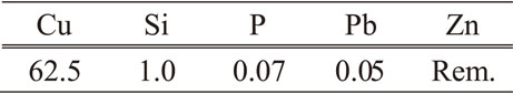
Table 1 Component of developed alloy (mass%).
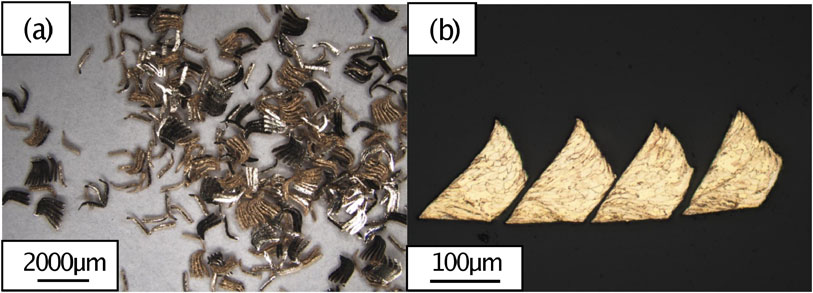
Figure 8 shows the chips of the developed alloy generated by turning and a cross section of one of them. These chips are thin shear type chips having an even thickness and a length of about 1 mm that are more similar to those of C3604 than those of β-brass containing 1 mass% Si and 0.07 mass% P. The thickness, the shape, and the size of the chips are also similar to those of C3604. The cutting resistance of the developed alloy is 125N, which is almost the same as that of the β phase containing 1 mass% Si and 0.07 mass% P, and about 25% higher than that of C3604. The cause of this is considered to originate in the tensile strength of the developed alloy, discussed below, that is about 30% higher than that of C3604.

From the fact that the developed alloy contains about 55% α phase, a phase having poor machinability, yet generates shear type chips that are finer and have a more even free surface than those of a β-brass containing 1 mass% Si and 0.07 mass% P, it is considered that the α phase with poor machinability is playing a major role. It is presumed that due to the presence of moderately dispersed soft α phase of about 10 µm in diameter, the hard β phase whose machinability is dramatically enhanced by Si and the fine phosphorous compounds uniformly distributed in the β phase are better acting as a stress concentration source during cutting, facilitating generation of shear type chips having an even thickness. Further, as shown by Fig. 7(b), it is expected that presence of α phase also has an effect of increasing the concentration of Si in β phase.
4.2.3 Cutting example using commercial cutting machine
Figure 9 shows some cutting samples made with the developed alloy using a commercial cutting machine applying the conditions approximately the same as those applied when cutting a commonly used alloy, C3604, and the chips generated during the cutting. The developed alloy can not only be turned, but also be machined in other ways such as threading, drilling, end milling, and knurling, and the generated chips are not bulky, i.e., they are easy to handle. In addition, no particular problems were found with dimensional accuracy of the product or tool wear after cutting 1,000 pcs for each model.
4.2.4 Mechanical and physical properties
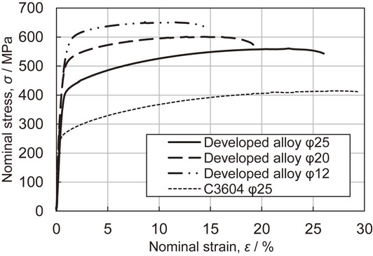
Table 2 shows typical physical and mechanical properties of the developed alloy. Typical stress-strain curves are shown in Fig. 10.

Table 2 Physical and mechanical properties of developed alloy.
The density of the alloy is 0.2 g cm−3 lower than that of C3604, and its electrical conductivity is higher than that of C5191, a phosphor bronze widely used in electrical and electronic components. The developed alloy has a tensile strength and a proof stress that are about 1.3 times higher than those of C3604 as well as a good ductility. Therefore, it is expected that the alloy is able to contribute not only to elimination of lead but also to a reduction in the size and weight of electric/electronic and automotive parts.
As described above, we have succeeded in developing a next-generation lead-free brass which is an α + β brass like a typical lead brass, C3604, but does not contain Pb or Bi yet has good machinability and mechanical and physical properties. Now that this newly developed brass is added to a list of available Pb-free brasses, replacement of free-cutting leaded copper alloys with Pb-free counterparts is expected to be realized in many fields and in many applications. It should be particularly noted that recycling of this alloy is easy since it is a Cu–Zn–Si–P alloy like C6932.
5. Conclusion
-
(1)
If a β-brass contains Si, which lowers stacking fault energy, thin shear type chips are produced during cutting which allows a reduction in cutting resistance. Phosphorous compounds act as a stress concentration source during cutting, promoting stable generation of shear type chips and their fragmentation.
-
(2)
In the developed alloy, due to the presence of moderately dispersed α phase with a grain size of 10 µm, β phase whose machinability is dramatically enhanced by Si, and the fine phosphorous compounds present in the β phase better act as a stress concentration source during cutting, allowing stable generation of shear type chips and breakup of the chips into smaller pieces.
-
(3)
It was confirmed in a test production using a commercial cutting machine performed under the cutting conditions of C3604 that the developed alloy can not only be turned but also be machined in other ways such as threading, drilling, end milling, and knurling, and that the chips are easy to handle.
-
(4)
The developed alloy has a lower density and about 1.3 times higher tensile strength than C3604. It is a next-generation lead-free free-cutting α + β brass that can not only contribute to elimination of lead but also to a reduction in size and weight of electrical and electronic parts and automotive parts.
REFERENCES
- 1) Öko-institut and Fraunhofer-institut IZM: “Assistance to the Commission on Technological Socio-Economic and Cost-Benefit Assessment Related to Exemptions from the Substance Restrictions in Electrical and Electronic Equipment, Final Report”, (2016) 338–368.
- 2) Öko-institut: “8th Adaptation to scientific and technical progress of exemptions 2(c), 3 and 5 of Annex II to Directive 2000/53/EC (ELV), Final Report”, (2016) 22–41.
- 3) K. Oishi, T. Matsumoto and T. Okubo: J. Jpn. Copper Brass Res. Assoc. 39 (2000) 8–15.
- 4) K. Oishi, I. Sasaki and J. Otani: Mater. Lett. 57 (2003) 2280–2286. doi:10.1016/S0167-577X(02)01211-9
- 5) K. Nakayama: The Metal Cutting in its Principle, (Corona Publishing Co., Ltd., Tokyo, 1978) p. 94.