Microstructure of Materials
Local Crystallization of Amorphous Aluminum Oxide Thin Film Using Electron Beam Irradiation by SEM
2023 年 64 巻 1 号 p. 184-190
詳細
2023 年 64 巻 1 号 p. 184-190
Amorphous thin film thinned for transmission electron microscopy observation is reported to crystallize by electron beam (EB) irradiation of TEM. If thin film deposited on substrates can be crystallized by EB irradiation of scanning electron microscopy (SEM), new nanoscale devices can be fabricated such as electronic nanoscale circuits in amorphous thin films. Therefore, an amorphous AlOx (am-AlOx) thin film is deposited onto a Si substrate by atomic layer deposition (ALD) and point and area scan irradiation of EBs were performed by SEM. Then, structure and elemental analyses are carried out by TEM. Only the point EB irradiated area crystallized from the surface to the interface between am-AlOx and the Si substrate, and γ-Al2O3 appeared. Moreover, the oxygen content of the not irradiated area close to the irradiated area was lower than that of the not irradiated area far from the irradiated area. These results show that the EB irradiated area was positively charged by the emission of secondary and Auger electrons under point irradiation conditions, and that oxygen was supplied by attracting its negative charge to the EB irradiated area. Also, the electrostatic repulsion between positively charged atoms and the structure relaxation due to electron excitation were additional driving forces for the crystallization.

Miniaturization methods are an important technology for the development of field effect transistors (FET), storage memory and electronic wiring. In miniaturization methods, visible and/or invisible light lithography and electron beam (EB) deposition are employed.1–3) EB is used in various fields, including material analysis, material development, electric device fabrication, sterilization, and medical equipment.4–10) In material analysis EB accelerated at a high voltage over a few hundred V have been used in electron microscopy (EM) for observing the inside structure and surface of a material. In contrast, EB irradiation is reported to be able to crystallize amorphous materials. The Jenčič group prepared lamellas made from Si, Ge, GaP and GaAs by mechanical and solution polishing. They irradiated an amorphous part of the lamella with EB during polishing and confirmed crystallization of the amorphous area, caused by contact between the crystal and EB irradiation. Based on that result, they indicated that electron excitation by EB irradiation happened at the interface between the crystal and the amorphous area.11) Gurbán et al. irradiated electrons in amorphous Al2O3 on Si to research diffusion phenomena at the interface between Al2O3 and Si and confirmed the mutual diffusion of Al2O3 and Si. This diffusion phenomenon was described to happen due to electrons being excited by the EB irradiation at dislocations around the interface.12) Furthermore, local heating happened when excited electrons from the inner cores of the atoms lost their energy by electron-hole recombination and electron-phonon interactions, and that heat crystallized the amorphous material.13) Some reports indicate that heating (including Jule’s and Jule-Lens heating) by EB irradiation helps the crystallization of amorphous materials.14,15) An described the crystallization of thin Ge2Sb2Te5 during EB irradiation and that the crystallized area had an identifiable orientation against the EB irradiation direction.16) Nakamura et al. indicated that not only heating by EB irradiation but also electron excitation at the EB irradiation area of a Al2O3 thin film helped crystallization based on in-situ TEM observation during EB irradiation as well as temperature calculations.17) More EB irradiation crystallization reports exist.18) However, material, sample shape and irradiation conditions are different in all reports and the most common shape of the sample is a thin film lamella for TEM observation in those reports. If EB irradiation is applied in crystal material fabrication, it is expected that the target sample will be a substrate and scanning electron microscopy (SEM), which can be used to scan with EB irradiation. In this study, a thin film deposited onto a Si substrate was irradiated with EB by two different irradiation methods, i.e., point and area scans, and the effects of the scan methods on the structure of the thin films were researched.
An amorphous AlOx (am-AlOx) thin film was selected as target for EB irradiation. When am-AlOx crystallizes, various crystal structures with different oxygen contents are formed.19) Research on the crystal phase generated by EB irradiation introduced the diffusion of oxygen ions and the temperatures of the substrate during EB irradiation as important factors, therefore, am-AlOx was selected as the sample deposited thin film. Am-AlOx was deposited by atomic layer deposition. The Si (100) substrate had a thickness of 0.5 mm with an area of 10 mm × 10 mm inserted into the ALD reaction chamber. The reaction chamber was evacuated to 3 × 10⁻⁵ Pa by a turbo molecular pump, then, that pressure was increased and kept at 25 Pa via N2 gas flow during the deposition process. After that the substrate temperature was increased and maintained at 200°C with a heating stage, then, trimethylaluminum (TMA) was used as Al source and H2O vapor as oxidation gas source, which were alternatingly transported into the reaction chamber along with a N2 gas flow. TMA was pumped into the chamber for 10 ms and then, the atmosphere inside the chamber was purged by a N2 gas flow for 20 s. Subsequently, H2O was used for 500 ms, then, N2 was introduced to purge the chamber. This sequence was defined as one cycle of depositing an am-AlOx single layer onto the substrate, and 1000 cycles were carried out. After deposition, substrate heating was stopped, and the substrate was left to naturally cool in the reaction chamber under N2 gas flow. Then, evacuation was stopped, and the chamber pressure was increased to atmospheric pressure by the introduction of N2.
The deposited substrate was taken from the reaction chamber and irradiated with an electron beam (EB) by conventional scanning electron microscopy (SEM, S-3000H, Hitachi). SEM was also used to observe the surface conditions of the substrate, and the energy content ratio of the deposited am-AlOx substrate between Al and O was acquired by an energy dispersion spectroscopy (EDS) system installed in SEM. An accelerated voltage of 25 kV and a current density of 250 mA·mm−2 were used as EB irradiation conditions. Moreover, area scan irradiation and point irradiation were performed, furthermore, the total irradiated electron on unit area equaled 2.5 C·mm−2 for both irradiation types.
A lamella sample was prepared for TEM/STEM observation to analyze the structure inside the thin film of the EB irradiated sample using a focused ion beam (FIB-SEM, MI4000L, Hitachi, Japan) system and an ion milling system (PIPS 693, Gatan). A carbon film was selectively deposited onto the EB irradiation area of the substrate surface by FIB-SEM. Lamella, which can be observed with TEM of the cross section of the thin film, were taken from the EB irradiated area of the sample by a Ga ion beam irradiated by a FIB-SEM system, then, that lamella was picked up and attached to a Si micro pillar on an Mo thin foil by a micro sampling system on the FIB. After that the Ar ion beam was accelerated with 3 kV to irradiate the thin sample and remove any remaining Ga used for taking and picking up the lamella from surface. After that the Ar ion beam accelerated with 3 kV was irradiated to the thin sample and remove any remaining Ga formed during the FIB processing.
For structure analysis, TEM/STEM (ARM-200F, JEOL), which have a cold cathode electron beam emitter and were equipped with an electron energy loss spectroscopy (EELS, GIF Quantum, Gatan) system, were employed. Selected area electron diffraction (SAED) was acquired by TEM from the EB irradiated area of the thin film to reveal the crystallization of the acquired area, then, an annular dark field STEM (ADF-STEM) image was observed using the STEM mode to research the shape and place of the EB irradiated area. EEL spectra of the critical area around the EB irradiated area were acquired to reveal changes in oxygen content.
(a) SEM image, (b) EDS spectrum and (c) cross section ADF-STEM image with SAED acquired of the deposited thin film area of the as-deposited substrate are shown in Fig. 1. No uneven surface was observed in the SEM image (Fig. 1(a)), and it was obvious that a flat thin film of AlOx had been deposited by the ALD process. In Fig. 1(b), A signal at 1.7 keV was acquired from Si, and this signal was generated by the Si substrate. The composition of the thin film was calculated based on the EDS spectrum, and the composition rate between Al and O is 1.36, which is lower by about 0.07 compared with crystalline Al2O3. This EDS analysis result means that the ALD process using H2O as oxidized gas cannot perfectly oxidize the TMA absorbed onto the substrate. The AlOx thin film deposited by ALD was often reported to have a lower composition rate between Al and O than crystalline Al2O3.20) In the ADF-STEM image (Fig. 1(c)), the existence of a carbon protection layer, an AlOx layer with a thickness of 130 nm and the Si substrate were clearly observed from top to bottom of the image, respectively. A slightly bright contrast layer was observed at the interface between AlOx and the protection layer, and this layer is expected to be the Ga implant inside the surface of the AlOx layer after the carbon protection layer had been deposited. Moreover, only a hallow pattern without diffraction spots was observed in SAED, and it was clear that AlOx deposited by ALD is an amorphous structure. These results show that the deposited thin film has a lower oxygen content than crystalline Al2O3 and has an amorphous structure. This am-AlOx deposited substrate was irradiated with EB.

(a) SEM image, (b) EDS spectrum, (c) STEM image with diffraction pattern acquired from thin film area.
SEM images of the (a) point and (b) area scan EB irradiated substrate are shown in Fig. 2. A circular dark contrast area with a diameter of about 4.5 µm, which indicates contamination deposited by the influence of EB irradiation, was confirmed at the center of the images in Fig. 2. The contamination was made from carbon, which has a lower atomic number than Al and Si in the substrate, and the electron emission rate of carbon is lower than those of Al and Si. Hence, the contamination was observed as a dark circular contrast. Furthermore, the center area of the circular contrast in Fig. 2(a) became brighter than the surrounding area. This means that the contamination with a higher center grew especially under point irradiation. A dark point contrast with a diameter of 0.75 µm in Fig. 2(a) and a rectangular, brighter contrast area with an area of 2.3 µm × 3.2 µm in Fig. 2(b) were also confirmed at the center of the contamination; arrows are used for visibility. These two different shape contrasts are expected to indicate point and area EB irradiation. As EB sputtered contamination, the contrast of the EB irradiated point and the area is thought to have different contrast compared around.
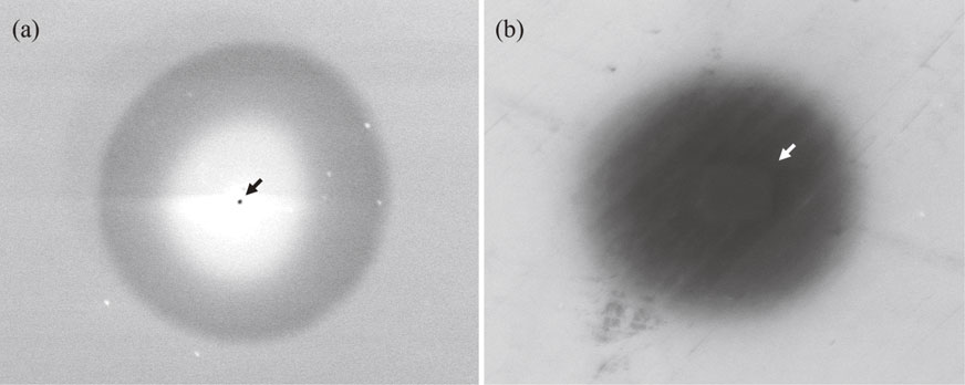
SEM images of (a) point EB irradiated substrate and (b) area scan EB irradiated substrate.
Cross section lamellar include point and area EB irradiated substrates, which are shown by arrows in Fig. 2 and were picked up by FIB-SEM and observed by STEM. Figure 3(a) and (b) show the cross section ADF-STEM images with inset diffraction patterns of the point and area scan EB irradiated thin film areas. Small grain contrast appeared in the deposited am-AlOx area with a width of about 0.78 µm for the point irradiated substrate in Fig. 3(a). However, a homogeneous contrast was confirmed for am-AlOx irradiated under the area scan condition, as shown in Fig. 3(b). The width of the small grain contrast area is similar to the diameter of the irradiated point, as confirmed in Fig. 2(a). This area was present from the surface of the am-AlOx layer to the interface between the am-AlOx layer and the Si substrate. Moreover, the thickness of the irradiated and not irradiated AlOx layers are different from that of the point irradiated substrate, 120 nm and 130 nm respectively. If EB irradiation sputtering leads to a decrease in thickness, this phenomenon should be observed in the area scan EB irradiated substrate with the same dose rate. However, the thickness of the deposited layer in the area EB irradiated substrate is 130 nm, and this result indicates that the thickness decrease of the point irradiated area did not happen due to EB irradiation sputtering. The edge shape of the small grain contrast area is not parallel to the EB direction but curved and leads from the EB irradiation area to the outside. In addition, the width of the small grain contrast area at the surface of am-AlOx is confirmed to be smaller by 200 nm than at the interface between am-AlOx and the Si substrate. The EB converged at the surface of the observed material due to an electromagnetic lens, so the EB spread after being incident on the observed sample.21) Hence, the shape of the crystallized area suggests the path of EB in the observed sample. The range of the small grain diameter is from 30 nm to 60 nm, is not uniform and does not depend on the depth from the surface of am-AlOx. Furthermore, diffraction spots, which were not observed in the insets of Fig. 1(c) and 3(b), appeared in the SAED pattern in Fig. 3(a). The spots do not have an array pattern but have a ring pattern, therefore, a polycrystal was formed in the point EB irradiated area by spot EB irradiation. In contrast, the halo-pattern in the diffraction pattern means an amorphous structure was confirmed, as shown in the inset of Fig. 3(b). These results show that area scan EB irradiation cannot transform the phase of the am-AlOx layer and that the grains appearing due to point EB irradiation have a crystalline structure. Then, the plane distance of the formed grains was calculated to deduce the crystal phase from the diffraction pattern shown in Fig. 3(a). Plane distances of 0.28, 0.24 and 0.20 nm were found and these number are almost equal to the (220), (311) and (400) face spacings of γ-Al2O3 (PDF ICDD 00-047-1292). The reported density of am-AlOx deposited by ALD is about 2.5 g·cm−3 which is lower than the density of crystalline Al2O3 at 3.65 g·cm−3.22,23) Hence, the reason for the thickness of the point EB irradiated area being smaller than that of the not irradiated area is thought to be that the density of the am-AlOx layer became higher due to crystallization in the γ-Al2O3 phase. Furthermore, other phases apart from γ-Al2O3 were not confirmed.

Cross-section TEM images of (a) point EB irradiated substrate and (b) area scan EB irradiated with diffraction pattern acquired from inside broken circle.
The aforementioned results are thought to indicate that EB irradiation causes crystallization of the AlOx layer. However, crystallization was confirmed only for the point irradiated sample, and did not happen for the area scan irradiation. Subsequently, possible reasons for the different outcomes of the two methods are discussed. For the crystallization of am-AlOx with a low oxygen content, oxygen had to be supplied from the vicinity of the EB irradiated area to the EB irradiated area. If oxygen was supplied from near the EB irradiated area, the oxygen content of the area near the EB irradiated area should be lower than that of areas far from the EB irradiated area.
Therefore, EELS was acquired from areas close to and far from the point irradiated area of the am-AlOx layer to determine the oxygen supply source. The Al-L2,3 edge of the EEL spectrum indicates bonding between Al and O in the am-AlOx layer, and especially the intensity of 77 eV and 80 eV in Al-L2,3 indicate an octahedral and tetrahedral structure with 6 and 4 coordinated oxygens for AlOx, respectively.24) Crystalline α-Al2O3, which is perfectly oxidized AlOx, has an octahedral structure. Therefore, a comparison of the intensity rates between 77 eV (IT) and 80 eV (IO) indicates the number of oxygens inside the AlOx layer.
The ADF-STEM image and EELS spectra of the point irradiated sample are shown in Figs. 4(a) and (b). In Fig. 4(a), the carbon layer for ion beam protection, the point irradiated and the not irradiated am-AlOx layer, and the Si substrate are confirmed. Especially, the left side bright area in the AlOx layer signifies a crystalized area. EEL spectra were acquired from three points of the ADF-STEM image. Each point, A, B and C was located near the crystalized area and two further points were 150 and 300 nm away from point A. In the EEL spectra of Fig. 4(b), the intensity at 77 eV and 80 eV indicates the existence of an octahedral and tetrahedral coordination of the Al ions, respectively, then, the intensity of around 83 eV corresponds to the spinel structure of Al2O3. The amount of am-Al2O3 is described to be comparatively smaller than the intensity of the crystal Al2O3.25) IT/IO are 0.61, 0.56 and 0.57 at point A, B, and C, respectively and the intensity rate at A is larger than that at the other points. This difference means that the oxygen content of the areas located close to EB irradiated areas decreased. Moreover, this decreased oxygen content is due to diffusion of the oxygen to the directly EB irradiated area, where it was used to crystallize the am-AlOx layer. Moreover, it is clear that oxygen diffusion mainly happened near the crystallized area.
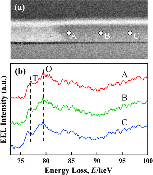
(a) ADF-STEM image and (b) EELS spectra acquired from points A, B and C of the irradiated AlOx thin film.
The driving force for the oxygen supply from the amorphous area to the point irradiated area is discussed below. SEM shows the morphology of the sample surface by detection of SE ejected from the sample surface, and SE released from atoms. When core electrons are excited by incident electrons, Auger electrons are released in addition to SE. Atoms have a positive charge when SE and Auger electrons is ejected from atoms. Oxygen ions with a negative charge are attracted to a positively charged area. The point irradiated area was supplied by oxygen ions from the not-irradiated area. Therefore, the oxygen content of the not-irradiated area near the irradiated area was expected to be lower than that of not-irradiated areas located far from the irradiated area. Furthermore, important results on the effects of differences in irradiation methods on crystallization should be considered. Defective Al2O3 has a high oxygen ion conductivity,26) and oxygen ions were supplied to this positively charged area from near the EB irradiated area. Ionic bonds were constructed, then, am-AlOx crystallized. In the case of area scan EB irradiation, EB can re-irradiate the same point after about 0.03 s because an image refresh rate of 30 Hz was employed in this study. The positive charge of the irradiated area became neutral when it receives electrons from the stage connected to ground while it is not irradiated with EB. So, the oxygen ion was not strongly attracted. However, in the point irradiation condition, the substrate is continuously irradiated to a single point and the charge of the irradiated area cannot be neutral. Hence, the point irradiated area has a continually positive charge during irradiation, then, the positive charge of the point irradiated area attracts oxygen ions from close to the area of the am-AlOx layer.
Oxygen exists not only inside am-AlOx but also in the atmosphere of the SEM chamber, and there is a possibility that oxygen was also supplied to the crystallized area from the atmosphere on top of the thin film. Furthermore SE, which is ejected from the substrate by EB irradiation and has an energy of a few tens of eV works to ionize the oxygen molecules in the atmosphere.27) Ionized oxygen was expected to present in the form of radicals. Total dose per unit area is equal for the point and area scan irradiation conditions, therefore, the number of generated ions per unit area is equal. There is a possibility that ionized oxygen from the atmosphere is supplied to the am-AlOx layer from the surface, however, the fact that the amorphous and crystal phases appeared for both irradiation conditions, suggests that ionized oxygen does not directly induce crystallization of am-AlOx. From EELS analysis, the oxygen content of am-AlOx around the crystallized area is lower than that of areas far away, and therefore, the main oxygen supply source is thought to be the amorphous area near the crystalized area.
A supply of oxygen ions alone surely cannot induce crystallization, and a driving force for crystallization is therefore needed. Below, possible reasons for the crystallization of am-AlOx are discussed.
Three factors are expected as driving forces for the material rearrangement necessary for crystallization. One is EB irradiation heating. Generally, an amorphous thin film is transformed into a crystal by heating.28–31) In the case of the am-AlOx thin film, it was reported that heating to over 820 K induced the formation of γ-Al2O3 and that α-Al2O3 was formed by heating to over 1270 K.32–34) The possibility of heat production by EB irradiation was considered in this study. Philippe et al. suggested eq. (1), shown below, for the increase in temperature of the EB irradiation area, and this equation can be used to calculate the highest increase in temperature for EB irradiated material.34)
| \begin{equation} \Delta T = \{3UI_{p}(1-\eta)\}/\{2\pi\kappa (R_{e}/2+D)\} \end{equation} | (1) |
Next, another expected driving force is electron excitation. EB usually used for SEM observation have enough energy, i.e., over a few hundred eV for the electron excitation of materials. When the sample was irradiated by EB, electrons in the electron orbitals in the material were excited to a higher energy level. If electrons in occupied deep level orbitals are excited to antibonding orbitals, the bonding length of the atoms becomes longer. That phenomenon can easily cause a structure relaxation, and then, crystallization could be a consequence for the EB irradiated am-AlOx layer.
Another driving force is electrostatic repulsion between charged atoms. As in the above discussion, when the material is irradiated with EB, secondary and Auger electrons are surely released from the atoms in am-AlOx and the atoms have a positive charge. In the case of area scan irradiation, the electron supply to positively charged atoms from the stage while other position of the substrate is irradiated by EB scanning, and positively charged atoms become soon neutral. However, for the point irradiation condition, the atoms are positively charged due to continuous irradiation. The positively charged atoms are repulsed by each other due to electrostatic repulsion in the EB irradiation area. There is a possibility that repulsion by electrostatic repulsion works as a driving force for atomic dispersion. If electrostatic repulsion is the main cause of this phenomenon, materials which can be crystallized by EB irradiation will be limited to insulators. Cazaux described that only insulator can be positively charged because these elements have no conductive electrons and cannot restore the electrical neutrality.37)
From among the three expected driving forces, the weakening of the bonding force between atoms due to electron excitation and electric repulsion between ionized atoms are thought to induce the material rearrangement for crystallization.
In the past, there were reports of crystallization of am-AlOx by EB irradiation. Murray irradiated a cross section thin film of Al with EB, an am-AlOx and Pt layer stacked and deposited by sputtering, and crystallization of am-AlOx was confirmed once a diffraction pattern was acquired from am-AlOx.15) Based on the result that crystallization of am-AlOx near Al, which has a high thermal conductivity, is lower than that in areas far from Al, thermal generated EB irradiation was expected to increase crystallization of am-AlOx in this instance. Moreover, Nakamura also confirmed that EB irradiation, which was accelerated at 25–300 kV, can crystallize am-AlOx deposited by an evaporation system. They reported lower energy EB need lower electron dose for crystallization.17) Furthermore, they deposited the low melting point material of In onto am-AlOx and observed that the deposited In did not melt during EB irradiation. They introduced the possibility that not EB irradiation heating, but electron excitation helps crystallization of am-AlOx based on these results. Klingshirn also described a similar relationship as Nakamura reported between the electron dose and electron energy for crystallization.38) The EB irradiated sample in this study was a substrate and is different from the TEM lamella used as samples in past research. A comparison between the above result and this study is difficult. However, according to the temperature calculation in this study the crystallization temperature of am-AlOx was not reached during EB irradiation. Moreover, the results that different irradiation conditions lead to differences in crystallization, suggest that irradiation excitation effectively works for crystallization. This study indicates that electron excitation, electric repulsion between positively charged atoms and diffusion of oxygen ions in am-AlOx appear due to continuous EB irradiation and are needed for the crystallization of am-AlOx. Furthermore, the crystallization time of am-AlOx is 10 s and changing the irradiation time was not tried. Then, crystallization of am-AlOx was observed for the EB point irradiation condition and not for the area scan condition with a refreshing rate of 30 Hz. Therefore, 10 s is expected to be enough time for oxygen ions diffusing from a not irradiated area to an irradiated area under the conditions in this study.
Based on the discussion above, the crystallization process of am-AlOx during EB irradiation described below was derived (Fig. 5). When the AlOx layer was irradiated by EB, SE and Auger electrons was released from the irradiated area and that area was charged positively. AlOx has good oxygen ion conductivity, thereby, oxygen ions were attracted to the positively charged area. As the oxygen ion supply from the am-AlOx layer is likely not enough, oxygen from the atmosphere was also used. Oxygen in the atmosphere was ionized by EB irradiation and/or SE released from the surface of the substrate and disassembled into oxygen radicals of atomic oxygen. These radicals were supplied to am-AlOx too. Moreover, the continuously irradiated area was not only positively charged but an excitation of electrons to anti-bonding orbitals was also expected. This electron excitation prompted a structure relaxation in am-AlOx. Furthermore, atoms in am-AlOx were positively charged by EB irradiation. Electrostatic repulsion between positively charged atoms in am-AlOx happened and also led to the structure relaxing. The supply of oxygen ions and the structure relaxation of am-AlOx induced crystallization, and γ-Al2O3 was formed. The distance of each atom in am-AlOx becomes uniform during structure relaxation and crystallization. The crystallization phenomenon was expected to stop when the atoms lost the driving force for relaxation after the appearance of γ-Al2O3.
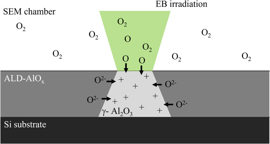
Schematic image of ALD-AlOx crystallization process by EB irradiation.
Results obtained from this article suggest a novel circuit equipment fabrication method by EB irradiation. For example, an EB irradiation process can be inserted after each cycle of the ALD process. An atomic layer is deposited by the ALD process, then, the local area is crystallized by EB irradiation accelerated to a low voltage of a few hundred V, at which EB can penetrate only a few nm. EB accelerated to a high voltage reaches a deep area and irradiated EB leave from irradiation axis like Fig. 4, therefore it is expected that only intended area cannot be crystallized by EB accelerated at high voltage. Through an ALD process with EB irradiation, a crystallized circuit, which is formed in the amorphous area deposited by the ALD process acting like a 3D printer, can be easily obtained. Materials with different electric and magnetic properties as the crystal and the amorphous structure can be adopted as ALD deposition material, and 3D structures with different properties on the nano and atomic level may bring the arrival of new devices.
In this paper, am-AlOx on Si substrate deposited by ALD was point and area scan EB irradiated, and the am-AlOx crystallinity of the irradiated area was evaluated. The structure of the irradiated area transformed from amorphous to crystalline only for the point EB irradiation condition. Moreover, only the γ-Al2O3 phase appeared in the irradiated area. The estimated EB irradiation heating cannot increase the am-AlOx temperature high enough for crystallization. These results indicate am-AlOx is crystalized by an EB irradiation effect other than EB irradiation heating. The charge of the irradiated area was expected to become positive by SE and Auger electrons release when am-AlOx was irradiated with EB. Positively charged atoms repulse each other, and this repulsion works as a driving force for atom dispersion for crystallization. Then, the electron excitations in atoms, which appear in am-AlOx due to EB irradiation, are thought to lead to a relaxation of the structure of am-AlOx. Moreover, positively charged areas in am-AlOx near the irradiated area attracted oxygen ions with a negative charge and there was a ready oxygen supply from the surrounding area. These driving forces and oxygen supply are thought to induce the γ-Al2O3 phase at the point irradiated area.