Microstructure of Materials
Local Crystallization of Amorphous Aluminum Oxide Thin Film Using Electron Beam Irradiation by SEM
2023 年 64 巻 1 号 p. 184-190
詳細
2023 年 64 巻 1 号 p. 184-190
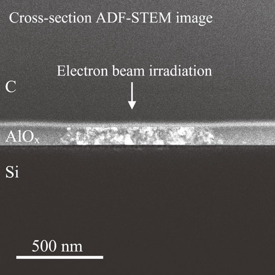
Amorphous thin film thinned for transmission electron microscopy observation is reported to crystallize by electron beam (EB) irradiation of TEM. If thin film deposited on substrates can be crystallized by EB irradiation of scanning electron microscopy (SEM), new nanoscale devices can be fabricated such as electronic nanoscale circuits in amorphous thin films. Therefore, an amorphous AlOx (am-AlOx) thin film is deposited onto a Si substrate by atomic layer deposition (ALD) and point and area scan irradiation of EBs were performed by SEM. Then, structure and elemental analyses are carried out by TEM. Only the point EB irradiated area crystallized from the surface to the interface between am-AlOx and the Si substrate, and γ-Al2O3 appeared. Moreover, the oxygen content of the not irradiated area close to the irradiated area was lower than that of the not irradiated area far from the irradiated area. These results show that the EB irradiated area was positively charged by the emission of secondary and Auger electrons under point irradiation conditions, and that oxygen was supplied by attracting its negative charge to the EB irradiated area. Also, the electrostatic repulsion between positively charged atoms and the structure relaxation due to electron excitation were additional driving forces for the crystallization.