1. Introduction
Thermoelectric (TE) materials have recently drawn considerable attention in renewable energy research for thermal management and utilization owing to their ability to directly convert waste heat into electricity.1,2) The efficiency of TE devices mainly depends on the dimensionless figure of merit ZT = S2σT/κ, where S is the Seebeck coefficient, σ is the electrical conductivity, T is the temperature, and κ is the thermal conductivity. These TE parameters are intercoupled because of the carrier concentration and band structure, which causes challenges in enhancing the ZT value by regulating any single parameter. Various effective strategies for improving TE parameters have been investigated, including phonon-liquid electron-crystal,3) distortion in the electronic density of states (DOS),4) nanostructure modification by alloying and doping techniques,5–7) quantum confinement effects,8) and electron energy barrier filtering.9) Combining these strategies have led to high TE performance in traditional materials, such as Bi2Te3, GeTe, and PbTe materials.1,2) Considering the large-scale deployment of TE devices in society, TE materials will have to simultaneously fulfill stringent requirements, such as non-toxicity, non-scarcity, and high efficiency. Therefore, new TE materials should focus on identifying Te-free TE compounds composed of low-cost earth-abundant elements.
Cu–S-based TE materials, such as liquid-like TE Cu2S,10) tetrahedrites,11–14) famatinites,15–18) colusites,19–22) and kesterites (stannites)23–26) are promising TE candidates owing to their environmental-friendliness and cost-effectiveness. Although these Cu–S-based “polycrystalline” materials typically exhibit ZT values of ∼1, we reported an environment-friendly kesterite Cu2ZnSnS4 (CZTS) “single crystal” with a ZT of 1.6.27,28) This result was achieved by exploiting the pseudo-cubic structure of CZTS, which led to low crystal-field splitting and a high power factor owing to degeneracy at the valence band maximum.29) Additionally, for single crystals with relatively low thermal conductivity (∼1 W/mK), the intrinsic Cu/Zn disorder in CZTS is a significant advantage.
Considering the significant role of thermal energy in a carbon-neutral society, the actual value of the TE conversion efficiency is required, rather than the enhancement of the ZT value. However, Cu–S-based TE devices have rarely been reported because of the considerable reactivity of S with metal electrodes, which limits the development of TE devices. Among Cu–S-based TE devices, a colusite-based single-leg TE device with an Au diffusion barrier layer between the TE material and Cu electrode achieved a conversion efficiency of 3.3% at a temperature difference of 273 K.30) Therefore, the properties of the TE material–electrode interface should be comprehensively investigated to develop Cu–S-based TE devices.
This study aims to demonstrate an effective TE single leg based on environmental-friendly kesterite CZTS with a high ZT value. We investigated the interface between CZTS and the contact metal, including chemical stability, enabling effective conversion efficiency, and long-term stability. Maximum conversion efficiency of 4.0% was achieved at a temperature difference of 473 K, thereby demonstrating the potential of CZTS for low-cost TE power generation.
2. Experimental Procedure
2.1 Fabrication of CZTS-based single-leg TE device
Our previous study revealed that Cu-poor compositions and Na doping led to a high TE performance owing to the shallow acceptor Cu vacancies and enhancement in the DOS in CZTS, respectively.28,31) In this study, the 5% Cu-poor and 0.1 mass% Na-doped CZTS single crystal was grown by Sn-solvent traveling heater method (THM).32,33) A diamond blade was used to dice CZTS single crystals to a leg size of approximately 5 mm × 5 mm × 10 mm. The TE legs were mechanically polished with 0.01 µm Al2O3 powder and subsequently etched with an HCl solution for 5 min to remove the saw and polishing damage. The Au barrier layer evaporated on both the top and bottom sides of the leg. Both sides and the Cu electrode were attached using Ag paste via heat treatment at 250°C for 1 h in an N2 atmosphere, which this structure was used for sulfide-based TE device.30) The CZTS-based single-leg TE structure was not scaled, as shown in Fig. 1.
2.2 Characterization
The orientation and crystallinity of the CZTS single crystals were investigated using X-ray rocking curve (XRC) analysis (Panalytical X’Pert PRO). XRC measurements were performed at 45 kV and 40 mA with a step width of 0.002° using a Cu Kα radiation source. The detailed composition of the crystals was determined using inductively coupled plasma-atomic emission spectroscopy (ICP-AES; SHIMADZU ICPS-8100). The samples were dissolved in a mixture of HNO3 and HCl to facilitate the analysis.
A scanning electron microscope (SEM; SU-3500 Hitachi) equipped with energy-dispersive X-ray spectroscopy (EDX) detector was used to investigate the elemental composition at the interface between the CZTS and Au layer. The analytical certainty associated with the EDX profiling was within 0.5 at%.
The electrical conductivity σ and Seebeck coefficient S of the samples were simultaneously measured in a helium atmosphere at 300–800 K using a commercial system (ZEM3; ADVANCE RIKO). Thermal conductivity κ was calculated using the equation κ = λCpD, where λ is the thermal diffusivity, Cp is the specific heat capacity, and D is the density. The thermal diffusivity of the rectangular samples was measured using the laser flash method (Netzsch; LFA467), and the samples were coated with a thin layer of graphite to minimize errors due to the emissivity of the material. The specific heat capacities of the samples were determined using differential scanning calorimetry (DSC; Rigaku Thermo plus EVO2 DSCvesta). Densities in the 4.4 g/cm3 range were measured using the Archimedes method at 300 K in ultrapure water.
A four-probe technique was used to measure the electrical resistance of a single-leg CZTS device. A movable probe was used to measure the voltage along the sample length when an alternating current was applied across the leg. The conversion efficiency of the CZTS-based single-leg TE device was evaluated by measuring the electrical output power and output heat flow under vacuum (∼10−2 Pa) using a mini-PEM tester (ADVANCE RIKO). The uncertainty in the evaluation of the conversion efficiency was determined to be approximately 5%.
3. Results and Discussions
3.1 Quality of single crystal
The CZTS single phase was obtained in this study, and the details have been reported in our previous study.32) The quality of the samples for TE measurements was evaluated using the XRC method shown in Fig. 2. The curves have good symmetry and narrow full width at half-maximum (FWHM). The results of multipoint tests on different positions of the sample wafer show that the FWHM of the (004) diffraction peak is between 110 and 125 arcsecs.
The compositional homogeneity of single crystals was less than 3 at% throughout the ingot and wafer by EDX mapping, which was reported in our previous study.28) The concentration of the unintentional impurities detected by ICP-AES is summarized in Table 1, for which the quality of the single crystal was confirmed. Unintentional impurity concentrations were fairly low (less than several hundreds of ppb).

Table 1 Unintentional impurity levels detected by ICP-AES in the CZTS single crystal.
Figure 3 shows the temperature dependence of ZT evaluated by electrical conductivity σ, Seebeck coefficient S, and thermal conductivity κ, where each TE parameter was discussed in our previous study.28) The ZT for CZTS is ∼1.6 800 K, which is caused by its high electrical properties and relatively low thermal conductivity along the a-axis. Additionally, the high ZT was proven to be reproducible by conducting repeated measurements for ten thermal cycles; the values for each cycle was within 10%.
Current TE devices have been developed using Te-based materials, such as Bi2Te3 and PbTe, which result in high costs. A comparison of the costs of CZTS and state-of-the-art chalcogenides indicates that the CZTS cost (∼103 $/ton) is an order of magnitude lower than those of other Te-based TE materials.34) Environmental-friendly TE devices should be developed for large-scale fabrication.
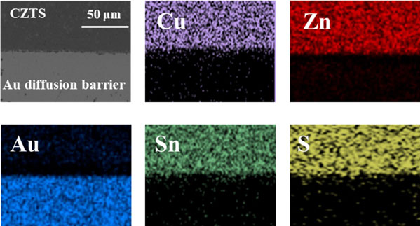
TE devices operating in the high-temperature range must be thermodynamically stable, and the TE material/contact interface is particularly important in this regard. Therefore, an Au layer was introduced as a diffusion barrier between CZTS and the electrode on both sides of the TE device because of the presence of mobile atoms, such as Cu, in CZTS. After a 100 h aging test conducted at 700 k, the hot-side interface was investigated to confirm the effectiveness of the Au layer as a diffusion barrier. Figure 4 shows a magnified SEM image and EDX elemental mapping images of the CZTS/Au interface. No secondary phases including Ag-related material were observed around the CZTS/Au interface; therefore, uniform chemical-diffusion-free elemental distributions were obtained. The ∼100-µm-thick Au diffusion barrier had a smooth interface with roughness undulations of several hundred nanometers.
According to the compositional results, Au is a good diffusion barrier for CZTS. TE devices can be optimized by minimizing the electrical contact resistance to ensure a low internal resistance. The total electrical resistance, including that of the Au diffusion barrier and Ag adhesive, was estimated using a four-probe technique at 300 K to be as low as ∼0.82 mΩ, shown in Fig. 5, which corresponded to an interfacial contact resistivity of ∼130 µΩ cm2. Although this value is higher than the benchmark established by the Bi2Te3–Ni interface (1–5 µΩ cm2),35) thermodynamic stability, that is, the relative change in the value in the range of 10% after the 500 h aging test at 700 K, is a more suitable characteristic for TE devices.
3.3 TE device properties
We investigated the power generation characteristics of a p-type CZTS-based TE single leg with an Au diffusion barrier. The output voltage (V), output power (P), output heat flow from the cold side (Qout), and conversion efficiency (η) were monitored as a function of the current (I) at different temperature gradients (ΔT) with a fixed cold-side temperature of 300 K (Fig. 6). The TE conversion efficiency (η) can be determined using eq. (1):
| \begin{equation}
\eta = \frac{P}{Q_{\text{in}}} = \frac{P}{P + Q_{\text{out}} + Q_{\text{rad}}}
\end{equation}
| (1) |
where
P,
Qin, and
Qrad are the generated power, input power from the hot side, and radiation loss from a single leg, respectively. The direct measurement of
Qin is challenging because of the heavy heat loss at high temperatures. The total
Qin value includes
P,
Qout, and
Qrad. Considering the minimization of radiation loss from the sides of the single leg, the samples were cut to a length of ∼10 mm and were well polished to increase the heat flow. The heat radiation loss can be ignored in this study, which is a typical determination of η values for reported TE single-legs.
36) In addition, the heat radiation loss of as much as 5% of the total heat flow can be estimated by the finite difference method.
37) Thus, the conversion efficiency formula is reduced to
(2).
| \begin{equation}
\eta = \frac{P}{Q_{\text{in}}} = \frac{P}{P + Q_{\text{out}}}
\end{equation}
| (2) |
This study, the TE conversion efficiency of the CZTS single leg was calculated using
eq. (2). The
y-intercept and slope of the linear
V–
I plots in
Fig. 6(a) enabled estimation of the open-circuit voltage (
VOC) and internal resistance (
Rin), respectively. All device parameters related to the maximum conversion efficiency are listed in
Table 2. The increase in
VOC and decrease in
Rin with increasing temperature can be attributed to the increase in
S and σ of CZTS, respectively.
28) The output power
P, in
Fig. 6(b) increases with increasing current, reaches a maximum when the external load resistance matches
Rin, and then decreases. The value of maximum output power
Pmax increased from 0.9 mW to 85.8 mW, thereby increasing the temperature gradient. The
Qout values increase with increasing electrical current at the respective hot-side temperatures, which is generally attributed to Peltier and Joule heating. A maximum efficiency η
max of 4% was achieved using an environmental-friendly CZTS device at a temperature gradient of 473 K, as shown in
Fig. 6(d), which is a kesterite-based TE device with reasonable conversion efficiency.
2)

Table 2 Measured and simulated open-circuit voltage (VOC), internal resistance (Rin), maximum output power (Pmax), open-circuit heat flow (QOC), and maximum efficiency (ηmax) of CZTS-based single-leg with different temperature gradients (ΔT).
The properties of the CZTS-based single-leg TE device were simulated using COMSOL Multiphysics software with a Heat Transfer Module using the measured Seebeck coefficient, electrical conductivity, and thermal conductivity. Figure 7 shows the simulated V, P, Qout, and η as functions of I using the model of the CZTS single leg. The simulated device parameters are listed in Table 2. The device parameters obtained from the simulation were in good agreement with the experimental results. The measured VOC values were lower than the simulated values at all temperature gradients in Fig. 7(a), possibly due to the temperature drop across the TE CZTS caused by the thermal contact resistance at the interfaces. In addition, the measured Rin values are larger than the simulated values because this simulation does not include the contributions of the contact resistance at the material interfaces and the resistance of the diffusion barrier layer to Rin. These results for Voc and Rin result in smaller experimental P values than the simulated values in Fig. 7(b). The y-intercept of the Qout-I plot in Fig. 7(c) is the open-circuit heat flow (QOC), which includes conductive and radiative heat, and the experimental values are higher than the simulated values. In this study, the experimental arrangement for the device properties had no shield to suppress radiative heat. The surface area of the heat source on the hot side is substantially larger than that of the single-leg device (approximately 5 mm × 5 mm), where the remaining open area provides radiative heat transfer to the cold side. Therefore, radiative heat transfer may result in higher experimental QOC values and an underestimation of η of the single-leg device, as shown in Fig. 7(d).

In addition to conversion efficiency, long-term thermal stability is a significant factor for TE devices. The various aging tests for the CZTS-based TE single-leg were conducted in an Ar atmosphere at 700 K. The TE single-leg was measured at a temperature gradient of 473 K after each aging test time, and each TE device parameter is shown in Fig. 8. The maximum increase in Rin was 15.5% after the 300 h aging test; however, no cracks were observed in the device by millimeter-scale optical microscopy. Generally, the Rin value for single-leg devices increases significantly with crack generation near the interfacial region. Further optimization of the device structure will improve its performance and stability. Based on these data, the present CZTS-based TE single-leg is sufficiently stable within several hundred hours.


