1. Introduction
Silicon (Si) is one of the most important semiconductor materials used in modern electronic devices, such as integrated circuits1) and solar cells.2) These Si devices are mainly fabricated using single- and/or poly-crystals with a diamond structure. However, the electronic structure of crystalline Si with an indirect bandgap of 1.12 eV hinders the wide range of device applications. Among several ways proposed to overcome this limitation, Si nanocrystals have attracted attention because photoluminescence associated with quantum confinement is realized in the visible light region.3,4) In addition, multiple exciton generation (MEG) is observed from colloidal Si nanocrystals,5) leading to the high-efficiency solar cells using Si nanocrystals. The Si nanocrystals can also be obtained by different methods, such as electrochemical etching,6) sputtering,7) ion implantation,8) and chemical vapor deposition.9)
Si allotropes are also of great interest because of their unique material properties.10) In particular, several metastable phases obtained by high-pressure phase transformations are promising because they are stable even at atmospheric pressure. According to high-pressure experiments, diamond-cubic (dc) Si-I transforms to tetragonal Si-II with a β-Sn structure at ∼11 GPa.11) Upon decompression, Si-II transforms to metastable Si-III with a body centered cubic (bc8) structure through rhombohedral (r8) Si-XII.12) The Si-III and Si-XII phases are also observed in indentation experiments onto Si substrates.13–15) Since Si-III and Si-XII have bandgaps of 30 meV16) and 0.24 eV,17) respectively, these metastable phases may become candidates for the future narrow gap semiconductor devices. In addition, Si-III nanocrystals are promising for solar cells with high conversion efficiency associated with MEG processes.18)
In order to realize the formation of nanocrystals and metastable phases of Si, we focused on severe plastic deformation (SPD).19–22) The SPD process has been studied not only for achieving ultrafine grained metals with excellent strength and ductility,23) but also for phase transformations.24,25) Among the various SPD methods such as equal channel angler pressing,26) accumulative roll-bonding,27) and high-pressure sliding,28,29) high-pressure torsion (HPT)30–33) constrains the sample in the cavity of the anvils under high pressure. The HPT processing is applicable to a wide range of materials, including metals,25,34–36) carbon,25,37) polymers,38) ceramics,39–42) and semiconductors.25) In the case of semiconductors, the HPT processing of Si and Ge has been studied earlier.43–46) We have further investigated the HPT processing of Si,47–53) Ge,54–56) and GaAs,57) and summarized them in previous overview papers.58,59) However, the phase transformations of the metastable phases in the HPT-processed Si during annealing as well as that of HPT processing at Si-I stable pressure (<11 GPa) have not been fully understood so far. In addition, little work has been reported on the formation of metastable phases in SiGe alloys.60,61) This overview paper focuses on recent HPT studies of Si and Si0.5Ge0.5 alloy, and further discusses their phase transformations and electrical, thermal, and optical properties.62–64)
2. Experimental Procedures
HPT experiments were performed using single-crystal Si(100) wafers and bulk-crystal Si0.5Ge0.5 grown by the traveling liquidus-zone (TLZ) method.65–71) They were cut into disks having a diameter of 5 or 10 mm, and placed on the lower anvil made of tungsten carbide with a hole having a depth of 0.25 mm and a diameter of 5 or 10 mm. The HPT facility are described elsewhere.72) All the HPT experiments were conducted at room temperature. The nominal pressures were set at 24 and 6 GPa for 5-mm and 10-mm diameter disks, respectively. The rotational speed was set at 1 rpm. The HPT-processed samples were characterized by x-ray diffraction (XRD) with the Cu Kα radiation. The phase transformation of HPT-processed Si during annealing was observed in situ by synchrotron high-energy XRD analysis with a photon energy of 61.4 keV at BL04B1 of SPring-8 in JASRI. The detailed procedures for the in-situ synchrotron XRD are described elsewhere.62,73) Photoluminescence (PL) measurements were performed at room temperature with a laser operating at a wavelength of 488 nm. Electrical resistivities were measured by a four-probe method with a probe distance of 1 mm. The thermal conductivity κ was calculated by
| \begin{equation}
\kappa = \alpha c\rho
\end{equation}
| (1) |
where α is the thermal diffusivity,
c is the heat capacity, and ρ is the density. The thermal diffusivity α was measured by a laser flash method. The details of the thermal diffusivity measurements are described elsewhere.
53) The heat capacity was set at 0.71 J g
−1K
−1 from the literature.
74) The density of the HPT-processed samples was calculated from the volume fractions of Si-I, Si-III, and Si-XII.
3. Results and Discussion
3.1 In-situ synchrotron XRD of HPT-processed Si during annealing
For the synchrotron XRD measurements, we performed the HPT processing of 5-mm Si disks at a nominal pressure of 24 GPa for 10 anvil rotations (N = 10). The XRD profiles during annealing were obtained using a specimen sliced into strips having a width of ∼1 mm from the HPT-processed disk sample. Figure 1 shows synchrotron XRD profiles of the HPT-processed Si during annealing. The profile at room temperature consists of Si-I and metastable Si-III/XII. The diffraction peak intensities of the Si-I and Si-III/XII are almost constant up to 433 K. The diffraction peak intensities at ∼4.3° and ∼6.6° for Si-III/XII gradually decrease at 453 K. The diffraction peak at ∼3.5° for Si-III/XII becomes broad when the annealing temperature increases to 473 K, and it remains as a shoulder of ∼3.7° for Si-I (111) diffraction peak. In addition, a new peak at ∼4.0° appears at 463 K, and its intensity increases with increased annealing temperature. The shoulder and new peaks correspond to (010) and (011) for Si-IV having a hexagonal diamond (lonsdaleite) structure. The Si-III/XII diffraction peaks disappear and the profile consists of Si-I and Si-IV after annealing at 473 K for 20 min.

In order to confirm the formation of Si-IV in the HPT-processed Si after annealing, we performed high-resolution transmission electron microscopy (HRTEM) observation of an ex-situ annealed sample at 473 K for 2 h in a nitrogen atmosphere. Figure 2 shows the HRTEM image and FFT patterns of the HPT-processed Si after ex-situ annealing. The polycrystalline ring patterns in the FFT pattern taken from the whole image indicate the presence of Si-I and Si-IV nanograins. The FFT patterns taken from square regions in the HRTEM image in Fig. 2 also correspond to Si-I or Si-IV structures.

The formation of Si-IV has been observed by phase transformation from Si-III at ∼473 K in indentation13) and in high-pressure experiments.75,76) as well as by double twinning of Si-I.77) On the other hand, no evidence of Si-IV was observed after annealing the nanoindented zone in crystalline Si.78) The observed difference indicates that the formation of Si-IV is sensitive to shear strain and annealing conditions. In the case of HPT-processed Si, we found the decrease of the Si-III/XII diffraction peak intensity and the appearance of Si-IV peaks with increasing the annealing temperature, as shown in Fig. 1. Since the volume fraction of Si-XII is less than 0.1 under the same HPT-processing condition,51) the observed Si-IV is mainly formed by the phase transformation from Si-III. It should be noted that the Si-I and Si-IV diffraction peaks and nanograins in Fig. 1 and Fig. 2, respectively, are also consistent with the x-ray photoelectron study of HPT-processed Si, in which a shift of the valence-band edge spectra occurred due to the mixture of Si-I and Si-IV after annealing.52) Since Si-IV is expected to be a semiconductor with an indirect bandgap of 0.95 eV,17) it will be a possible light absorber for solar energy conversion.79) These results suggest that the combination of HPT processing and low-temperature annealing can be effective in the formation of novel metastable phases.
3.2 HPT processing of Si at nominal pressure of 6 GPa
It is well known that metastable Si-III/XII phases are obtained by phase transformation from high-pressure Si-II upon decompression.12) When shear strain is applied to Si under high pressure, the phase transformation from Si-I to Si-II occurs at lower pressure than under hydrostatic conditions.80,81) In the case of HPT processing, Si-I → Si-II phase transformation at lower pressure (<11 GPa) and Si-II → Si-III/XII phase transformation upon decompression can be expected to occur due to a large amount of shear strain. We thus performed the HPT processing at a nominal pressure of 6 GPa for various number of anvil rotations (N) using 10-mm diameter Si disks.63) Figure 3 shows XRD profiles of HPT-processed Si for N = 10, 50, and 100. Weak diffraction peaks corresponding to Si-III/XII appear at ∼33° and 52° as well as Si-I diffraction peaks for N = 10. The intensities of the Si-III/XII diffraction peaks increase with increasing N, while those of the Si-I diffraction peaks decrease with increasing N for 50 and 100. The average crystallite sizes estimated by Rietveld analysis using a crushed specimen are of the order of 10 nm for N = 10, and decrease to ∼10 nm for Si-I and Si-III, and <10 nm for Si-XII when N ≥ 50. Figure 4 shows the volume fractions of Si-I, Si-III and Si-XII with respect to N. The HPT-processed Si consists mainly of Si-I for the case of N = 10. The volume fraction of Si-I decreases to ∼0.5 when increasing N to 100, while that of Si-III increases to more than 0.3 with increasing N. The volume fraction of Si-XII saturates at ∼0.2 for N = 100.
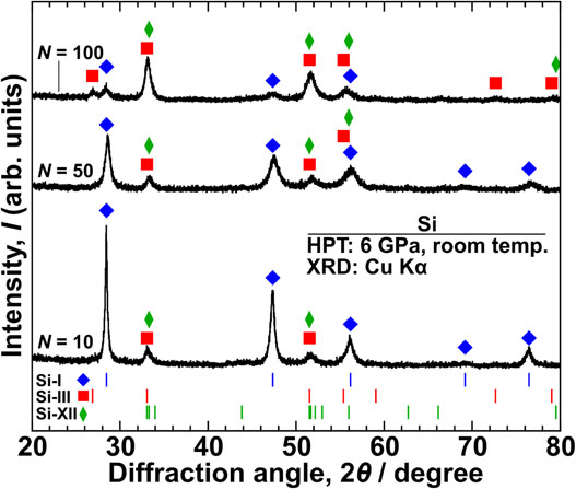
The formation of Si-III/XII as shown in Figs. 3 and 4 indicates that the strain-induced phase transformation from Si-I to Si-II occurs during HPT processing under the nominal pressure of 6 GPa. The shear strain γ of the HPT processing is calculated by31)
| \begin{equation}
\gamma = \frac{2\pi rN}{t}
\end{equation}
| (2) |
where
r is the distance from the disk sample center,
N is the number of anvil rotations, and
t is the thickness of the disk sample. The increase in the volume fraction of Si-III indicates that the formation of metastable phases is enhanced by shear strain. It should be noted that the formation of Si-XII is less observed in the high-pressure experiments using a diamond anvil cell,
82) but is often observed in indentation experiments.
83) In the case of HPT processing, we found that the volume fraction of Si-XII increases to ∼0.2 with increasing the imposed shear strain, as shown in
Fig. 4.
The formation of metastable phases and grain refinement affect the electrical and thermal properties. Figures 5 and 6 show the changes in resistivity and thermal conductivity, respectively, with respect to the HPT processing. The resistivity in Fig. 5 increases from 0.2 to ∼0.5 Ω m after HPT processing for N = 10, but decreases to ∼2 × 10⁻² Ω m after N = 50. The resistivity further decreases to ∼7 × 10⁻³ Ω m for N = 100. The thermal conductivity of bulk Si at ∼140 W m−1K−1 (Ref. 84)) decreases to the order of 10 W m−1K−1 after HPT processing for N = 10, and further decreases to ∼3 W m−1K−1 as N increases to ≥50, as shown in Fig. 6.
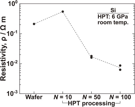
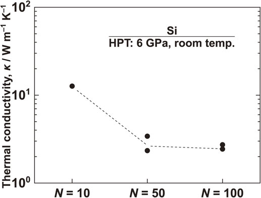
Such changes in the resistivity and thermal conductivity are attributed to the grain refinement and the formation of metastable phases. The resistivity of metals after HPT processing generally increases with increasing the imposed shear strain due to grain refinement.85) The opposite trend has been observed in the case of HPT processing of Si at the nominal pressure of 24 GPa,51) due to the formation of semimetallic Si-III.76,86) The resistivity changes in Fig. 5 indicate that its increase for N = 10 and subsequent decrease for N ≥ 50 are due to the grain refinement and the increase in the volume fraction of Si-III, respectively. The significant reduction in the thermal conductivity is also observed in nanostructured Si.87,88) The thermal conductivities of Si-III and Si-XII at 300 K are theoretically calculated to be 4 and 19 W m−1K−1, respectively.53) The reduction in thermal conductivity as shown in Fig. 6 is due to the grain refinement and the formation of Si-III/XII, as in the case of HPT-processed Si at the nominal pressure of 24 GPa with the thermal conductivity of 5–7.6 W m−1K−1.49,53) The saturation of the thermal conductivity at ∼3 W m−1K−1 when N increases to ≥50 indicates that the grain refinement is the major factor in the reduction of thermal conductivity in this case.
The HPT processing also affects the optical properties of Si. Figure 7 shows typical PL spectra of the samples after HPT processing at the nominal pressure of 6 GPa for N = 50 and following annealing at 873 K. No appreciable PL peak is observed at most of the measurement points after HPT processing while a weak broad PL peak in the visible light region appears occasionally after annealing. The appearance of the PL peak after annealing has also been observed in the case of HPT processing at the nominal pressure of 24 GPa.47,48) The absence of PL from HPT-processed Si indicates a large amount of lattice defects in the HPT-processed sample. Since the diffraction and Raman peaks of the HPT-processed Si after annealing at 873 K correspond to Si-I,63) and since no appreciable grain coarsening occurs by annealing at 873 K,50) the weak broad PL peak in Fig. 7 originates from Si-I nanograins due to quantum confinement.3,4)
3.3 HPT processing of Si0.5Ge0.5
SiGe alloys have been extensively studied for high-mobility metal-oxide-semiconductor field effect transistors,89) quantum well structures,90) and thermoelectric devices.91) The development of SiGe metastable phases may open up new device applications because the bandgap can be changed not only by the Ge concentration (x) but also by crystal structures. The phase transformation of SiGe alloys under high pressure has been studied experimentally92,93) and theoretically.94–97) Recently, Serghiou et al.60) reported that bc8-Si1−xGex was obtained by high-pressure (17 GPa) and high-temperature (1500 K) experiments using a multi-anvil cell for 0 < x < 0.76. They also reported that tetragonal st12-Si1−xGex appeared for x > 0.76.60) The st12 phase is known to be metastable Ge-III formed by decompression of high-pressure tetragonal Ge-II.98–100)
More recently, hexagonal Si1−xGex was obtained using multi-anvil and laser-heated diamond anvil methods.61) However, the formation of metastable phases in SiGe alloys has not been studied so far. In order to investigate the metastable phases of SiGe alloys, we utilized homogeneous bulk Si0.5Ge0.5 crystals obtained by the TLZ method,67–71) and performed HPT at the nominal pressure of 24 GPa using 5-mm diameter disks. Figure 8 shows the XRD profiles of the HPT-processed Si0.5Ge0.5 samples after compression (N = 0) and for N = 10. The diffraction peaks of the sample for N = 0 correspond to the dc structure. Additional new peaks as well as dc peaks appear when N increases to 10. These new peaks correspond to bc8-Si0.5Ge0.5 with a lattice constant of 0.678 nm. The lattice constant is in good agreement with Vegard’s law (0.6784 nm) using the lattice constants of 0.6636 nm for bc8-Si (Si-III) and 0.6932 nm for bc8-Ge (Ge-IV).101) Figure 9 shows the HRTEM image of the HPT-processed Si0.5Ge0.5 sample for N = 10. The FFT pattern obtained from the whole image corresponds to dc and bc8 structures. The FFT patterns taken from the square regions indicate that nanograins with dc and bc8 phases are present in the HPT-processed Si0.5Ge0.5 sample.


The formation of bc8-Si0.5Ge0.5 as shown in Figs. 8 and 9 is consistent with the high pressure and high temperature experiments reported by Serghiou et al.60) In the case of HPT processing of Si0.5Ge0.5, the phase transformation from dc to high pressure phases such as a β-Sn phase at ∼12 GPa92) and an Imma phase at ∼18 GPa96) during compression, and the phase transformation from the β-Sn phase to bc8 upon decompression are expected to occur. We have not observed other metastable phases such as r8- and st12-Si0.5Ge0.5 in the HPT-processed Si0.5Ge0.5 samples as shown in Figs. 8 and 9. It should be noted that r8-Ge is observed in the indentation experiments at low temperature,102,103) and the volume fraction of Si-XII is low in the case of HPT processing of Si at room temperature as shown in Fig. 4. The formation of st12-Si is predicted when depressuring from Si-II at high temperature,104) and is experimentally obtained using the ultrafast laser-induced confined microexplosion.105) Since the HPT process is performed at room temperature, the formation of bc8-Si0.5Ge0.5 is consequently the dominant metastable phase in the present case.
In order to examine electrical properties, we measured the resistivity of the HPT-processed Si0.5Ge0.5 samples. Figure 10 shows the changes in the resistivity with respect to HPT processing. The resistivity increases from ∼9 × 10⁻⁵ Ω m to ∼5 × 10⁻⁴ Ω m after N = 10, and decreases slightly as N increases to 10, despite the grain refinement. The decrease in resistivity after HPT processing is similar to the case of HPT processing of Si as shown in Fig. 5, where semimetallic Si-III with a bc8 structure is formed.51,63) It should be noted that bc8 Ge-IV is obtained by rapid pressure release from Ge-II,101) and is expected to be semimetallic.106) These results indicate that bc8-Si0.5Ge0.5 is semimetallic, similar to Si-III and Ge-IV.


