Regular Papers
Metal-induced Work Function Modulation of Single-layer Graphene Characterized by Kelvin Probe Force Microscopy and Raman Spectroscopy
2025 年 23 巻 2 号 p. 108-112

詳細
2025 年 23 巻 2 号 p. 108-112
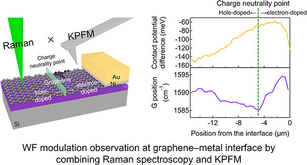
The semiconductor–metal interface is critical for optimizing the performance of semiconductor devices. For instance, low-resistance Ohmic contacts are essential for high-performance devices like field-effect transistors, while the performance of Schottky junction-based devices, such as diodes and photovoltaics, depends on the formed Schottky barrier height. Generally, the barrier height at the interface does not directly correspond to the work function difference between the semiconductor and metal, showing the difficulty on achieving these devices with ideal performance; this issue persists even for two-dimensional (2D) materials such as graphene and transition metal dichalcogenides. Therefore, developing a reliable method to evaluate the 2D material–three-dimensional metal interface is crucial. In this work, we report an evaluation of the graphene–Ni interface using Kelvin probe force microscopy (KPFM) and Raman spectroscopy. By combining these techniques, we found that the Ni contact exhibited electron doping into graphene, in contrast to the commonly observed hole-doping at graphene–metal contact. We speculate that this discrepancy arises from charge transfer from Ni. Our results emphasize the importance of utilizing KPFM and Raman spectroscopy for a deeper understanding of the graphene–metal interface.