Abstract
The application of semiconductor nanocrystals containing cadmium, lead, selenium and mercury as constituent elements is strictly limited by concerns about environmental pollution and health effects. Nanocrystals free of these toxic elements are being pushed to the forefront of nanocrystal research because of their environmentally friendly advantages and attractive photophysical properties on recent advances in colloidal synthesis, excellent optical properties, optoelectronic device applications, and biological applications of these environmentally friendly fluorescent nanocrystals. In this context, the first topic in this review paper introduces group IV semiconductors. In particular, the unique light emitting properties generated in silicon nanocrystals of diameters smaller than bulk exciton Bohr radius are highlighted. Next the topic turns to the nanocrystals of group III–V semiconductors. After that, attentions are paid to the lead-free perovskite nanocrystals such as tin-based halide perovskite and double perovskite structures. Recent efforts on how to control nanostructures to enhance photoluminescence quantum yields is highlighted for each semiconductor nanocrystal. Finally, the remaining challenges that must be overcome to realize nontoxic optoelectronic devices will be discussed.
1. Introduction
Colloidal semiconductor nanocrystals have attracted huge interests over 30 years. The nanocrystals contain hundreds to thousands of atoms and are covered with organic molecules (i.e., ligands) to make them stabilize in solution (Calvin et al., 2022), providing high accessibility to printable technology. They are called “quantum dots (QDs)”, “artificial atoms” or “zero-dimensional quantum boxes”. The effect of quantum confinement happens for the nanocrystals of diameter smaller than the bulk exciton Bohr radius for the bulk crystal. QDs are usually larger than the conventional organic dyes but comparable to fluorescent proteins and other large biomolecules. Their optical properties are unique and can be adjusted with diameter, chemical composition, shape, and surface state. Therefore, the QDs as optically active sources have a strong potential for use in a variety of optoelectronic applications including light-emitting diodes, photodiodes and photovoltaics as well as in biomedical detection such as fluorescence cellular imaging. In a typical, a single QD contains atoms of group IV elements (e.g., Si, C or Ge), group II–VI elements (e.g., CdS, CdSe, CdTe, ZnS, ZnSe or ZnTe), group III–V elements (e.g., InP, InSb or InAs), group I–III–VI2 elements (e.g., CuInS2, CuInSe2, AgInS2 or AgInSe2), group IV–VI elements (e.g., PbS, PbSe or PbTe), ZnS–AgInS2 (ZAIS) or AgInSe2–ZnSe (ZAISe). The QD as a core could be often encapsuled with additional protective shells of ZnS and/or ZnSe, which are well-known wide-band-gap semiconductors, to form core/shell structures.
Metal-halide perovskite nanocrystals are optically active materials whose chemical compositions and structural spaces are constantly expanding for successive tuning of optical absorption and emission spectra. Lead halide perovskite has emerged as an attractive semiconductor material due to its excellent optical and electronic properties and is expected to find applications in a wide range of optoelectronic fields, including light-emitting diodes (LEDs). Until now, many efforts have been made to increase photoluminescence quantum yield (PLQY) to nearly 100 % in the visible and near-infrared regions by optimizing synthesis parameters, impurity doping, alloying and surface passivation (Chen et al., 2021a). Various high-performance optoelectronic devices with the lead perovskite nanocrystals as active layers have been investigated by taking advantage of these excellent properties (Quan et al., 2019). Thus, the lead halide perovskite nanocrystals are expected to be the next generation of light emitting devices, and the external quantum efficiency of lead-based LEDs exceeds 20 % (Lin et al., 2018). There are concerns of environmental pollution and health problems due to the toxicity of Pb. Recent studies have shown that the bioavailability of lead from lead halide perovskite is stronger than other sources of lead and that as the concentration of lead halide perovskite in plants increases, the capacity for lead uptake increases (Li et al., 2020). To overcome this short coming, lead-free perovskite nanocrystals such as tin halide perovskite or double perovskite nanostructures have attracted attention over the years. However, the luminescence performances of the lead-free perovskite nanocrystals currently far inferior to the lead perovskite ones.
Controlling the fate of free-charge carriers generated in nanocrystals of semiconductor through sequential absorption of photons in the photoexcited state determines optical performance (Chen et al., 2021b). For example, radiative recombination between electrons and holes should be strengthened to increase the PLQY. Furthermore, defective surface serving as electron trappers should be removed to decrease the nonradiative recombination rate (Ghosh et al., 2020). On the other hand, the formation of shallow energy levels is key to synthesize long persistent phosphors, which are a class of optical batteries, allowing emission of luminescence continuously for a long time after the removal of excitation sources (Liu Q. et al., 2021a). In this review, recent efforts on defect control to improve PLQY of typical non-toxic nanocrystals for optical applications such as light-emitting diodes with emission layer of QD (QLED), namely, electrically driven luminescent (EL) devices will be presented.
2. Group IV QDs
QDs in group IV semiconductors such as carbon, silicon (Si), and germanium have attracted attention in the applications of abundant and nontoxic fluorescence materials, with an emphasis on their role in optoelectronics and nanomedicine. This chapter presents the research advances in fluorescent SiQD on controlled nanostructures giving a strong light emission and various photonic applications such as light-emitting diodes, biomarkers for cellular imaging and photothermal therapy of cancer cells.
2.1 Improved PLQYs
Bulk Si crystal has an indirect band structure, which results in very low PLQY (<10−4 %). However, the situation changes drastically when crystals are nanosized to nanoparticles of 5 nm or less in diameter. In the electronic structure of 2–5 nm crystals, the quantum confinement effect of photoexcited carriers relaxes the momentum conservation based on the uncertainty principle (ΔχΔρ ≥ ħ/2) and interface scattering-induced Γ–X coupling, leading to the zero-phonon optical interband transitions (Lee et al., 2016). In the 1.1–1.7 nm crystal size range, a diamond cubic crystalline Si can behave like a molecule in terms of energy structure (Shirahata et al., 2020). The most conventional Si surface is terminated with hydrogen atoms (H-SiQD) as known from the wafer chemistry (Shirahata et al., 2005). Photoluminescence (PL) properties are dependent of the size of diamond cubic nanocrystal of Si. First, the peak position of the PL spectrum depends on the size of the H-SiQD and can be modulated over a wide wavelength range of 530–1050 nm as shown in Fig. 1(a)–(c). Second, the PLQYs monotonically increase with decrease in size of H-SiQD based on the quantum confinement effect (see Fig. 1(d)). PL peak positions at 1050 nm for the 5-nm diameter SiQD and does not shift to a longer wavelength side anymore for the diameter range between 5 and 8 nm. The hydrogen atoms may cover 99 % of the Si atoms in the outermost layer. In the oxidized SiQD, the electron-hole recombination involves O-related defect centers (Dohnalová et al., 2013). In contrast, the hydrogen termination minimizes surface oxidation that forms SiOx. Nevertheless, the resultant PLQYs are still less than 15 % as shown in Fig. 1(d). A significant increase in PLQY is realized by replacement of surface hydrogen atom with alkyl monolayer through the hydrosilylation reaction (see Fig. 1(d)). The best value of PLQY is more than 73 % for the near-infrared light emitting QD (Jurbergs et al., 2006). Two possible mechanisms have been proposed to explain the improved PLQY. Dohnalová et al. reported the theoretical studies of the change in radiation rate and recombination process due to the attachment of alkyl monolayers, which switches SiQD from an indirect-bandgap-like material to a direct-one, leading to the phonon-less character of excitonic recombination close to band edges (Poddubny and Dohnalová, 2014). The increase in radiative recombination rate resulting from the alkylation of surface Si atoms has also been reported (Mastronardi et al., 2012), consistent with the theoretical prediction (Lee et al., 2016). Furthermore, alkyl monolayers work to inhibit the formation of defects as a nonradiative channel in the outermost layer of QD. Specifically, combining scanning transmission electron microscopic (STEM) observation with Raman spectroscopy demonstrated that the hydrogenated surface layer is distorted under structural reconstruction to generate an amorphous phase (Ghosh et al., 2016), whereas the passivation with alkyl monolayers suppresses the surface reconstruction to hold a bulk-like geometry (i.e., a diamond cubic lattice structure) in a broad range from the center toward the near-surface in QD (Ghosh et al., 2018a). The amorphous region might have many dangling bonds as a nonradiative relaxation channel, resulting in a low PLQY, but there are few defects around the surface terminated with alkyl monolayers. This suggests that the passivation with alkyl monolayers works to prevent any undesired surface reconstruction, leading to high PLQY.

The tremendous improvement in PLQY has attracted interests of scientists and encouraged the fabrication of devices such as current-driven QLEDs in which alkyl terminated SiQD works as an active layer. The reported device architectures have a multilayer structure where SiQD are sandwiched between hole and electron transportation layers as shown in Fig. 2(a)–(c). The electroluminescence (EL) signals are observed under low applied voltage. Fig. 2(d)–(f) demonstrates that the EL spectral peak shape and broadness are similar with those of PL spectra. Besides, the photocurrent depends on applied voltage, leading to the increase of luminance at high device current density. The EL spectral peak position precisely tuned by diameter of SiQD. To date, the highest values of external quantum efficiency (EQE) at present were 4.8 %, 8.6 %, 3.36 %, 6.2 %, for the EL spectral peaking at 1000 nm (Watanabe et al., 2021), 853 nm (Cheng et al., 2011), 755 nm (Yamada et al., 2020), 720 nm (Ghosh et al., 2018), 700 nm (Liu X. et al., 2018), respectively. The EQEs of EL spectra peaking at the wavelength shorter than 700 nm are less than 1.2 % (Yamada et al., 2020). These values are still lower than 20 % which is commonly employed as a benchmark. Further improved EQE requires both improvement of carrier mobility and charge balance (Watanabe et al., 2021).

By taking advantage of the large Stokes shift between optical absorption and emission derived from SiQDs, a white-light EL is realized with a superimposed spectrum of a red EL peak and a blue–green EL peak without loss of optical energy (Ghosh et al., 2014). The high PLQYs are realized by various method such as nonthermal plasma (Kortshagen et al., 2016), annealing of Si-rich borophosphosilicate (Kano et al., 2018) and thermal disproportionation of hydrogen silsesquioxane (Dasog et al., 2016) or silicon monoxide (Sun et al., 2015). Hydrogen silsesquioxane are commercially available from Dow Corning Corporation (trade name FOx-17) but could be synthesized by hydrolysis and condensation of triethoxysilane (Chandra et al., 2017) or trichlorosilane (Sun et al., 2016).
2.3 Bio imaging and analysis
Inherently nontoxic element such as Si is expected to use for fluorescence labeling of cells or tissues. Wang et al. reported the first ever biomedical use of SiQDs as a fluorescence label for DNA (Wang et al., 2004). Since then, many papers have been reported on modifying the surface of QDs to give them water solubility (Xu et al., 2016). Swihart et al. further studied the labeling of cells with SiQDs and found that SiQDs can be used for in vivo imaging (Erogbogbo et al., 2010). Si as an element shows cell cytotoxicity but the toxicity is strongly influenced by surface terminal groups (Ruizendaal et al., 2009). Specifically, amine-terminated surfaces are known to have low cell viability, while carboxyl-terminated surfaces are less toxic to cells than amine-terminated ones, since most living cells are negatively charged. In many cases, amphiphilic molecules such as Pluronic F127 or PEG are employed to encapsulate the core of SiQDs because the PEGylated surface is electronically neutralized due to hydroxyl groups exposed on the QD surface (Chinnathambi et al., 2019) resulting in high hydrophilicity and biocompatibility (Hessel et al., 2010). Such a biologically inert surface demonstrates a potential for medical diagnosis without major conformational change of human blood plasma proteins in the bloodstream (Chinnathambi et al., 2020). Thus, water-soluble SiQDs have the potential to be used as fluorescent labeling materials for cells and tissues due to their low cytotoxicity, but there are still challenging topics in terms of optical properties. Specifically, PL spectra are dependent of QD size in the near-infrared (NIR) wavelength range, but SiQDs exhibit low absorption efficiency for NIR light. Therefore, it is difficult to realize NIR–NIR excitation-emission bioimaging in a single-photon excitation environment. There are two methods to overcome this difficulty. First one is the fluorescence imaging under multiphoton excitation conditions (He et al., 2008). The first multiphoton-excited fluorescence imaging of cells labeled with SiQD was reported in 2016 (Chandra et al., 2016). Second one takes advantage of long radiative decay time (~μs scale) originating from energy structure of SiQD. That is, the time-gated fluorescence imaging in the NIR wavelength range was investigated for the observation of biological tissues labeled with SiQDs (Sakiyama et al., 2018).
The Si surface exhibits high chemical affinity for covalent bonding with carbon, oxygen, and nitrogen, and can produce a variety of organic derivatives hybridized at the molecular level (Shirahata, 2011). Their bonding ability can be used for post-synthesis purification by gel permeation chromatography (Shirahata et al., 2010). During purification, QDs can be separated according to differences in PLQY (Watanabe et al., 2021).
2.4 Photothermal effect
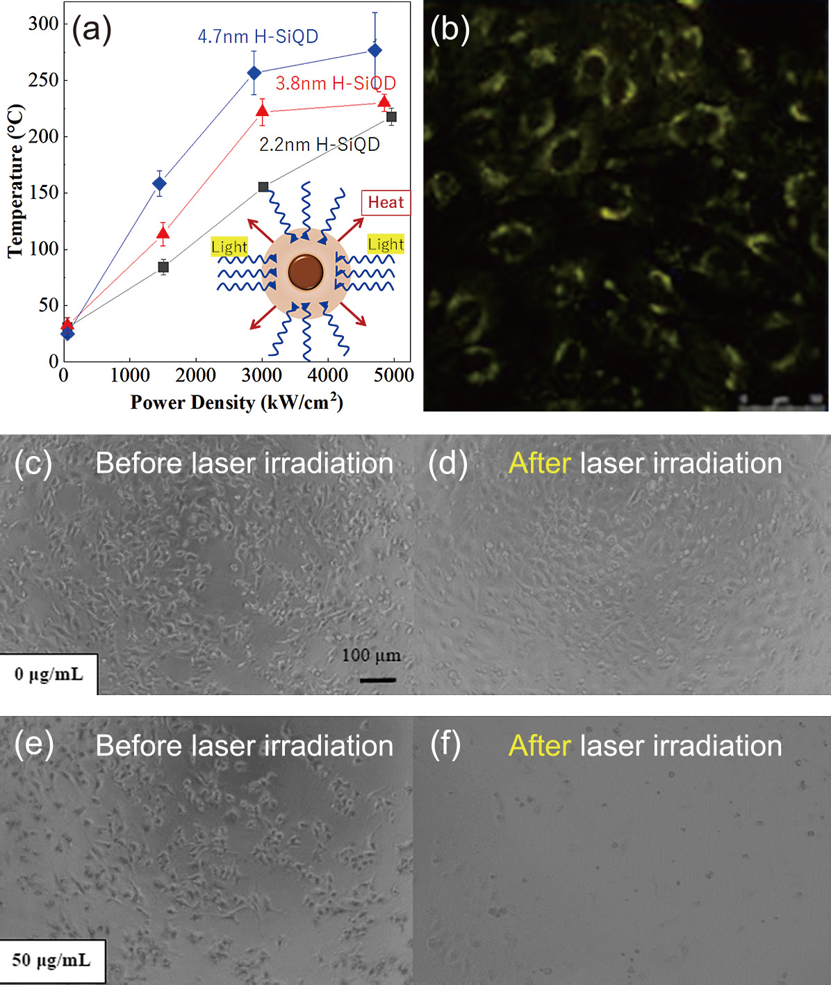
The photothermal effect refers to the ability to convert photon energy from light absorption into heat. Thermal conversion by photoexcited nanostructures can take place by different mechanisms depending on the nature of the material. Unlike metallic nanoparticles, for semiconductor QDs, photothermal conversion is explained by excess carriers undergoing nonradiative recombination, which is enhanced by maximizing the nonradiative decay rates and manipulating nonradiative channels. Controlling the heat of the QDs expands their availability for applications including phototheranostics and photoacoustic bioimaging. The photothermal responses of crystalline Si have been investigated for various forms, including nanoribbons, nanowires, films, porous particles, and nanoparticles. Multiple structural parameters such as size, surface configuration, and shape affect the photothermal response, but size is the most influential parameter. The temperature trend for larger crystals is explained by the Mie resonances (Ishii et al., 2016). As shown in Fig. 3(a), the photothermal response was dependent of size of QD even in the narrow range of 2–5 nm because the presence of a relatively high density of defect states for nonradiative thermal dissipation for larger QDs (Özbilgin et al., 2021). The photothermal conversion efficiency values of SiQDs are dependent of their sizes and estimated to be 25–37 % which are comparable to the nanoparticles of mesoporous Si (33.6 %), Au (13–21 %), CuSe (21 %) Fe/Fe3O4 (20.3 %), black phosphorus (24.8 %), Bi2S3 (28.1 %) or CdTe (14 %), suggesting a potential of SiQD available in photothermal applications. One example is demonstrated in the thermotherapeutic study where carboxy-terminated SiQDs internalized in the HeLa cell generates the heat to kill the cells under laser irradiation (Özbilgin et al., 2022). Fig. 3(b) shows the fluorescence image of HeLa cells labeled with the water-soluble red-light-emitting SiQDs, confirming the cellular internalization of the QDs. Furthermore, there is no significant change in cell morphology. Fig. 3(c) and 3(d) show the differential interference contrast (DIC) image where HeLa cells are observed throughout the microscope field of view. Without QDs, the cells remained the same even after laser irradiation as shown in Fig. 3(d). However, there was a noticeable decrease in the number of cells observed for the irradiated cells in which the QDs with even the concentration as low as 50 μg/mL are internalized. As evidenced in Fig. 3(f), the HeLa cells that take up the QDs detached from the glass substrate. A few cells remaining on the glass surface have also changed their morphology to round and have lost their adhesive ability. This result indicates that QDs can be effectively used for photothermal therapy. Controlling the nonradiative channels allows surgeons and medical/healthcare professions to manipulate the photothermal heating in a relatively lower temperature range, contributing to the development of therapeutic thermal phononics.
3. Group III–V QDs
Group III–V semiconductors are compounds formed between group III and group V of the periodic table and contain InN, GaN, GaAs, InP, InAs and InSb. Group III–V semiconductor devices are used as high electron mobility transistors due to their high electron mobility and electron density, which are essential for high-speed device operation. For example, InN is a semiconductor with a narrow band gap of about 0.7 eV at room temperature. When combined with gallium to make the ternary alloy InGaN, the band gap is tuned in the range of 0.7–3.4 eV, covering the infrared to the UV. GaN offers a wide energy bandgap and attract the development of nitride based blue LEDs and ultraviolet laser diodes. Bulk crystal of InP has a 1.35 eV of bandgap at room temperature, and its bulk exciton Bohr radius and exciton binding energy are 11 nm and 6 meV, respectively. Therefore, QD of InP crystal has attracted attention for the spectral tunability of the emission and the first exciton peak of absorption in a wide visible wavelength range. This chapter describes recent strategies for structural control of InP QDs to obtain high PLQY for optoelectronic applications.
3.1 Improved PLQYs
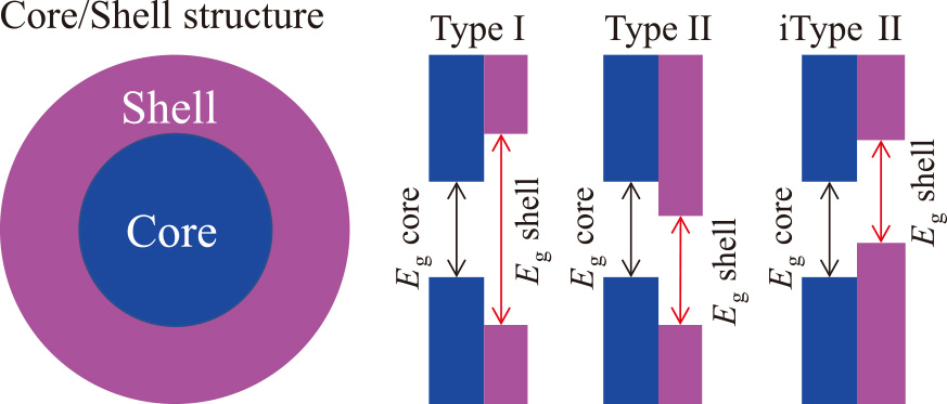
To improve PL performance, it is necessary to eliminate surface defects, which work as nonradiative exciton recombination centers (Coughlan et al., 2017). In a typical, a semiconductor core/shell structure is employed to reduce defects such as electron traps at the interface as depicted in Fig. 4 (Reiss et al., 2009). A core QD (e.g., indium phosphide, InP) is encapsulated by another semiconductor shell whose band gap (Eg) is large enough for sandwiching that of the core QD. Such a core/shell heterostructure is referred to as a Type I band alignment. In this configuration, excitons are spatially confined to the core, minimizing their interaction with surface states, and preventing their diffusion throughout the core/shell QD due to high energy barrier of shell Eg (Tamang et al., 2016). This confinement strength allows for enhanced radiative recombination rates and high PLQY. A good example of Type I architecture is InP/ZnSe/ZnS core/shell/shell structure. In the bulk state, direct deposition of ZnS (lattice constant, aZnS = 0.541 nm) on InP (aInP = 0.587 nm) results in a large lattice mismatch of 7.8 %, sufficient to cause defect formation at the heterogeneous core/shell interface and relaxation of the mismatch by lattice distortion is no longer thermodynamically feasible because of lattice mismatch relaxation. There are three approaches to solve this problem. First is to use the ZnSe (aZnSe = 0.566 nm) as the shell material; the lattice mismatch (≤3.5 %) between ZnSe and InP is reduced compared to the case of ZnS, so an energy-graded core/shell interface is constructed, and defect generation is suppressed. As a result, PLQY is significantly enhanced up to unity (Wu et al., 2020). Second, multielement alloying for the core (e.g., InxZnyP) is effective to mediate the lattice strain at the heterogeneous core/shell interface, leading to the improved PLQY. As expected, the strategy of alloying core has inspired the concept of compositional alloying between Se and S or Mg and Zn for shell materials (Lim et al., 2013). In the InP/GaP/ZnS core/shell/shell system, the strain energy that would have been induced at the interface between the inner shell and core is relaxed by cation exchange. During high-temperature synthesis for shell formation, Ga3+ ions diffuse into the core and are alloyed by replacing In3+ ions. This alloying QD achieves a PLQY as high as 80 % by continuously changing the chemical composition and reducing the strain energy at the interface (Srivastava et al., 2018). Third, Nemoto et al. reported an interesting idea of using material strain to build a QD with a coherent core/shell structure (Nemoto et al., 2022). Specifically, the core/shell QD allowed both epitaxial growth of the shell layer and distortion of the spherical core, changing the intrinsic interatomic distance of each crystal for coherency, where the core crystal is elastically compressed, and the shell crystal is stretched by lattice distortion to a lattice constant similar with that of the core. As depicted in Fig. 5, the coherent growth of ZnS on a InP core QD yields InP/ZnS core/shell structure with a single lattice constant of 0.563 nm. Compared to the bulk crystal of zinc-blend (cubic) InP, the lattice of the core QD is compressed by 4.1 %. In contrast, the lattice of the shell expands by 4.1 % relative to the bulky ZnS crystal throughout the core/shell QD. This could be because the change in lattice constant due to stress is thermodynamically more favorable than the formation of defect trapping sites at the core/shell interface to release strain energy. As expected, PLQY is enhanced up to 70 % and PL spectrum is also as narrow as 36 nm.
The first QLED that exceeded the benchmark was reported in winter of 2014 and used CdSe as the active layer of the device, emitting red light (Dai et al., 2014). The second QLED exhibited the green EL with 20 % EQE and had CsPbBr3/MABr quasi-core/shell structure as the active layer (Lin et al., 2018). InP-based QDs as optically active layers are the most promising alternative Cd- and Pb-free QLEDs. Since the innovative work of the first InP-QLED in 2011, intensive efforts have produced visible light emitting QLEDs. Finally, in 2019, Jang et al. reported blue, green, and red emitting QLEDs with 20 % of EQE using InP/ZnSe/ZnS QDs as active layers (Won et al., 2019).
Photoelectrode is also one of the optoelectronic applications. It is expected to realize the wavelength tunability of detected light by taking advantage of size dependence of the first exciton peak in the optical absorption spectrum, but not yet reported before due to possible difficulty in dissociation of photogenerated carriers into electrons and holes. Do-Hyun Kwak et al. reported a phototransistor with a light absorbing layer of InP QD in the hybrid structure of InP QD/black phosphorus. They replaced the oleylamine on the QD surface with 1,2-ethanedithiol (EDT), which has a shorter alkyl length, by ligand exchange to improve the carrier mobility and enhance device characteristics (Kwak et al., 2019). Under violet-light illumination, the photogenerated electrons from the InP QD layers are quickly transferred to the BP transport layer, resulting in a high photo response of 109 A/W and a high detectivity of 4.5 × 10¹⁶ Jones.
4. Lead-free perovskite nanocrystals
Lead halide perovskites are increasingly gaining attention for advanced optoelectronic applications due to their excellent optoelectronic properties, but there are two serious concerns for commercial use. First, metallic lead ions are readily soluble in water to cause ecological threats. Second, the current lead perovskite nanocrystals have been found to have low stability to UV irradiation, moisture, and heat. These disadvantages have stimulated the development of research into the colloidal synthesis of lead-free perovskite nanocrystals. This chapter presents recent progress in synthesis methods to enhance the PLQY of lead-free perovskite nanocrystals.
4.1 Cesium tin halide perovskite nanocrystals
Inorganic metal halide perovskites have a general chemical formula ABX3, where A is a monovalent cation (e.g., cesium, Ce+), B is a divalent metal ion (typically tin, germanium or copper), and X is a halide anion (Cl−, Br−, or I−). Tin halide perovskite exhibits a band gap of 1.2–1.4 eV, high carrier mobilities, and long carrier diffusion lengths (Pitaro et al., 2022). Therefore, nanocrystals of cesium tin halide perovskite structure (i.e., Cs2SnX3) are expected to be a representative of Pb-free perovskite nanocrystals. Owing to a large absorption coefficient and a wide bandgap-tunability between 1.3 and 2.8 eV, Cs2SnX3 has a potential of their use in various applications such as photovoltaics, photoelectrode and light-emitting devices (Chen J. K., 2021c). So far, the synthetic development of its nanocrystals lags far behind lead perovskite nanocrystals. As a result, their optical properties are also inferior to those of Pb-based materials; Jellicoe et al. reported that a higher density of trapped states results in lower PLQY (Jellicoe T. C. et al., 2016); Wong et al. pointed that Sn vacancies as the trap states work to lower PLQY (Wong et al., 2018). How to reduce defect density to obtain high PLQY? To answer this conundrum, Sun et al. proposed that precisely adjusting the ratios of starting precursors corresponding to Cs, Sn, and X over a wide range is crucial for suppressing the formation of lattice defects in CsSnX3 nanocrystals because the defect formation energy is closely related to the chemical potential of each component. Wang et al. tuned the molar ratios of precursors in a wide range to suppress the formation of defects contributing to nonradiative charge-carrier recombination and found that addition of the small amount of zwitterionic phosphatidylcholine as a surfactant in the reaction is crucial for controlling the growth rate of the nanocrystals (Wang et al., 2021). According to their experimental study, the growth rate of CsSnX3 nanocrystals was controlled by the formation of an intermediate complex between the zwitterionic phosphatidylcholine and the precursor and the steric hindrance effect of the branched fatty acid side chain of phosphatidylcholine. The resultant nanocrystal exhibited PLQY of 12.5 %.
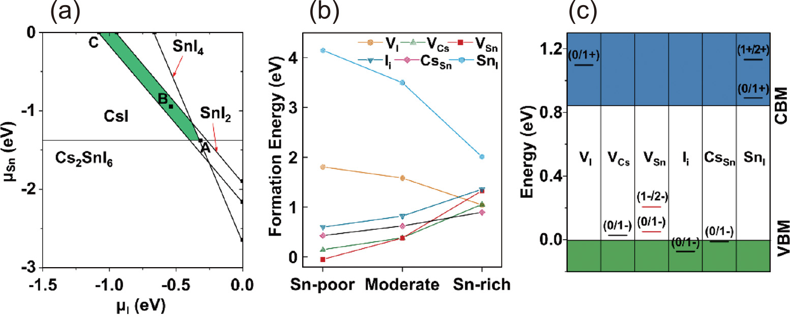
Great attention has more recently been paid to the colloidal synthesis guiled by theoretical studies using machine learning. In this context, Sun et al. investigated the formation energy and the thermodynamic charge-transition levels of typical point defects, as well as the influence of Sn vacancy on the photophysical properties based on density functional theory (DFT) calculations and molecular dynamics (MD) simulations (Liu et al., 2021b). Specifically, the stability regions of different compounds vs. I and Sn chemical potentials of CsSnI3 were calculated at the outset (see Fig. 6(a)). The result implied that the defect formation energy of CsSnI3 is sensitive to the chemical potentials of reactants. Then, the defect formation energies and defect charge-transition levels were calculated to show Fig. 6(b) and 6(c). Clearly, tin vacancies (VSn) introduced deep trap levels. Guided by this calculation result, CsSnI3 nanocrystals were colloidally synthesized through the careful tuning of the ratio of precursors. It was found that suppressing the Sn vacancy strengthens the increase of radiative recombination rate for enhanced PLQY along with a narrow emission spectral peak. By intentionally adopting a Sn-rich reaction condition, along with judicious choice of precursors with suitable reactivity, the resulting narrow-band-emissive CsSnI3 nanocrystals exhibit a record PLQY of 18.4 %. The development of synthetic methods, guided by computational science, will facilitate the study of tin-based perovskite nanocrystals and accelerate their application in high-performance optoelectronic devices such as solar cells, light-emitting diodes, and lasers.
Inorganic double perovskite crystals have a chemical formula, A2B(I)B(III)X6 where A is a monovalent cation (typically Ce+), B(I) is a monovalent cation (Ag+ or Na+), B(III) is trivalent cation (In3+, Bi3+ or Sb3+). Since the first report on the synthesis of lead-free double perovskite crystals, various chemical compositions of compound A2B(I)B(III)X6 have been investigated to tune the bandgap. For example, when Cl− (2.77 eV), Br− (1.95 eV), and I− (1.75 eV) are introduced as X sites in the Cs2AgBiX6 structure, the band gap decreases in that order (Creutz et al., 2018). Among the reported lead-free double perovskite structures, a bulk crystal of white-light emitting Cs2AgxNa1−xInyBi1−yCl6 double perovskite structure was reported to show a high PLQY of 86 ± 5 % (Luo et al., 2018). After that, the PLQY of Bi3+-doped Cs2Ag0.4Na0.6InCl6 microcrystals of about 10 μm in diameter was improved up to 97.33 % (Peng K. et al., 2022). From now on, the double perovskite crystals become a potential material for single-emitter layer applied in optical applications (Zhang et al., 2022). However, a dramatic decrease in PLQY resulting from nanostructuration happens due to the formation of defective structures.
Research to increase PLQY in nanocrystals has been intensively pursued recently. Here, a typical method to find the underlying mechanism of the enhancement of the PLQY is demonstrated using Cs2Ag0.65Na0.35InCl6 nanocrystal as an example. HR-TEM image shown in Fig. 7(a) demonstrates Cs2Ag0.65Na0.35InCl6 nanocrystals having a square shape and an average diameter of about 10 nm. The estimated PLQY was 3 %. Improvement of PLQY was realized by impurity doping of Bi3+ ions. Fig. 7(b) shows a typical HR-TEM image of the Bi-doped nanocrystals. When the 1 % Bi3+ ion was doped, the PLQY was enhanced up to 33.2 % (see Table 1). Fig. 7(c) shows PL spectra of the undoped sample measured in the temperature range from 20 K to 300 K. As clearly seen, the integrated PL intensity decreases with the increasing temperature monotonously possibly due to the thermal activation of the nonradiative channels present in the nanocrystals. Doping of 1 % Bi3+ ions suppressed the decreasing rate in PL intensity with temperature compared to undoped ones as shown in Fig. 7(d), suggesting the decrease of nonradiative channels. As summarized in Table 1, the nonradiative recombination rate (knr) was reduced by a factor of 15 in the doped sample compared to the undoped sample. The possible defects as the nonradiative channel identified by investigating the temperature-dependence of PL spectral linewidth combined with chemical composition analysis were indium vacancies generated in the crystal growth (Huang et al., 2022). The possible mechanism of enhanced PLQY was that Bi3+ ions occupy the indium vacancy to relax the strained lattice, yielding the decreasing number of nonradiative channels. Thus, spectroscopic studies at low temperatures provide structural insight into the cause of low PLQY.
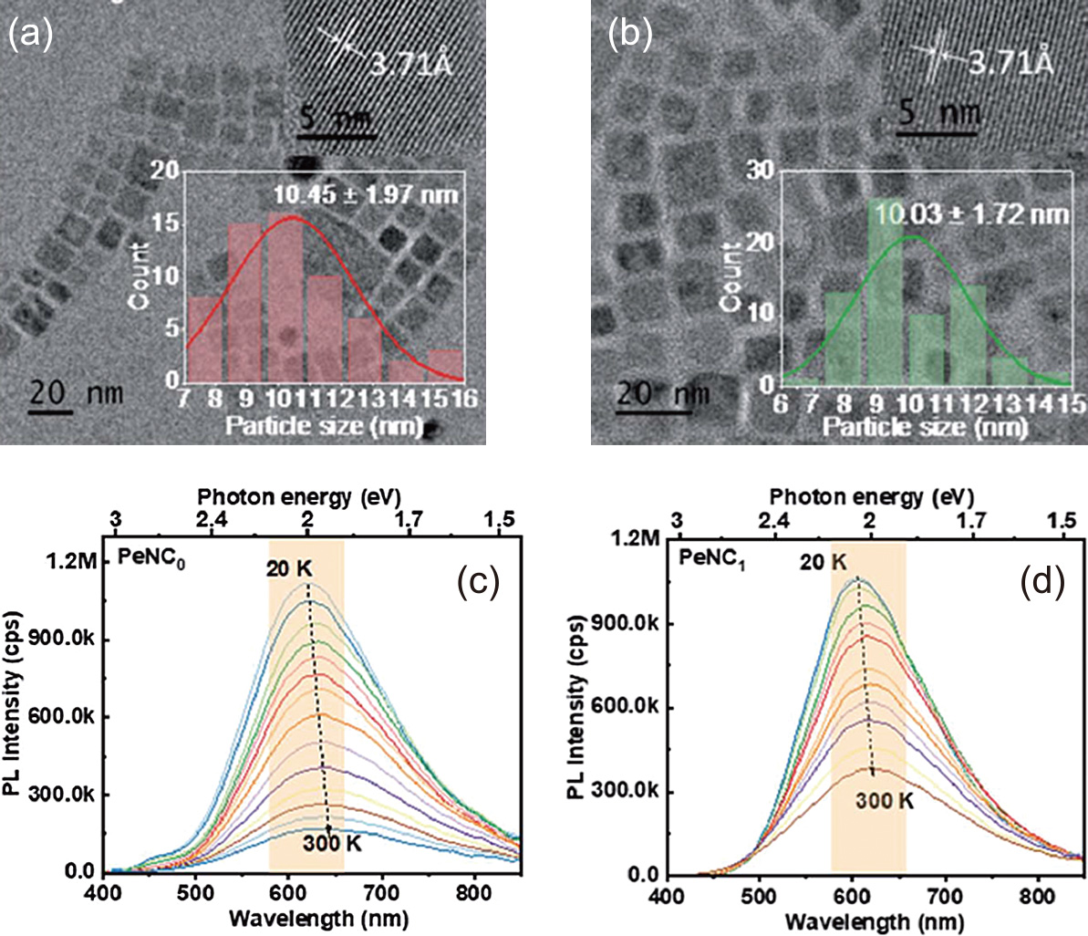
Table 1
PL decay parameters * of the Cs2Ag0.65Na0.35InCl6 doped with and without Bi3+ ions.
| Sample |
PLQY (%) |
kr a(μs−1) |
knr b(μs−1) |
R2 |
| Undoped |
3.0 |
0.13 |
4.20 |
0.99 |
| Doped |
33.2 |
0.14 |
0.28 |
0.97 |
a kr is the radiative recombination rate calculated by the formula:
kr = PLQY/
τ(avg).
τ(avg) means the value of average PL lifetime.
b knr is the nonradiative recombination rate calculated by the formula:
knr = 1/
τ(avg) −
kr.
* Other parameters for calculation are reported in the published paper (
Huang et al., 2022).
5. Summary
Driven by the toxicity concerns of cadmium, lead, mercury, and selenium, research on the synthesis of colloidal nanocrystals composed of nontoxic elements has made significant progress over the last decade. While previous studies have already detailed the synthesis and excellent properties of Cd- and Pb-based nanocrystals, non-toxic nanocrystals, the subject of this review, have not yet been fully described. The review was structured as follows: First, optical properties of SiQD were summarized. Due to their low absorption coefficients, they do not work as strong phosphors, but they find an application in the deice field of current driven LED because carriers are given from electrode and does not need absorbing the light. Second, InP was topicalized among III–V semiconductors. Metallic In is a small amount of constituent element on earth but does not exclude it from the discussion here. The pioneering work on red−green−blue (RGB) LEDs with beyond 20 % EQE spurs a lot of interests. Next target is narrowing of their EL spectra (<30 nm). For Pb-free perovskite nanocrystals, recent advances in colloidal chemical method were presented here. The journey to find experimental parameters to reduce defects has just begun. Much research is still needed to advance the field of non-toxic semiconductor nanocrystals. Although technological advances in synthesis methods, reports of prototype devices using light emission from nanocrystals, and even induced emission and nanobio applications have progressed over the past decade, it is safe to say that nanophotonics is still in its infancy.
Acknowledgments
This work was supported by WPI program, JSPS KAKENHI Grant-in-Aid for Scientific Research (B) Grant Number 21H01910 and The Murata Science Foundation.
References
- Calvin J.J., Brewer A.S., Alivisatos A.P., The role of organic ligand shell structures in colloidal nanocrystal synthesis, Nature Synthesis, 1 (2022) 127–137. DOI:10.1038/s44160-022-00025-4
- Chandra S., Ghosh B., Beaune G., Nagarajan U., Yasui T., Nakamura J., Tsuruoka T., Baba Y., Shirahata N., Winnik F.M., Functional double-shelled silicon nanocrystals for two-photon fluorescence cell imaging: spectral evolution and tuning, Nanoscale, 8 (2016) 9009–9019. DOI: 10.1039/C6NR01437B
- Chandra S., Masuda Y., Shirahata N., Winnik F.M., Transition metal doped NIR emitting silicon nanocrystals, Angewandte Chemie International Edition, 56 (2017) 6157–6160. DOI: 10.1002/anie.201700436
- Chen J.-K., Zhao Q., Shirahata N., Yin J., Bakr O.M., Mohammed O.F., Sun H.-T., Shining light on the structure of lead halide perovskite nanocrystals, ACS Materials Letters, 3 (2021a) 845–861. DOI: 10.1021/acsmaterialslett.1c00197
- Chen J.-K., Shirahata N., Sun H.-T., Metal-free scintillators excite X-ray community, Nature Photonics, 15 (2021b) 171–172. DOI: 10.1038/s41566-020-00751-1
- Chen J.-K., Zhang B.-B., Liu Q., Shirahata N., Mohammed O.F., Bakr O.M., Sun H.-T., Advances and challenges in tin halide perovskite nanocrystals, ACS Materials Letters, 3 (2021c) 1541–1557. DOI: 10.1021/acsmaterialslett.1c00444
- Cheng K.-Y., Anthony R., Kortshagen U.R., Holmes R.J., High-efficiency silicon nanocrystal light-emitting devices, Nano Letters, 11 (2011) 1952–1956. DOI: 10.1021/nl2001692
- Chinnathambi S., Karthikeyan S., Hanagata N., Shirahata N., Molecular interaction of silicon quantum dot micelles with plasma proteins: hemoglobin and thrombin, RSC Advances, 9 (2019) 14928–14936. DOI: 10.1039/C9RA02829C
- Chinnathambi S., Hanagata N., Yamazaki T., Shirahata N., Nano-bio interaction between blood plasma proteins and water-soluble silicon quantum dots with enabled cellular uptake and minimal cytotoxicity, Nanomaterials, 10 (2020) 2250. DOI: 10.3390/nano10112250
- Coughlan C., Ibáñez M., Dobrozhan O., Singh A., Cabot A., Ryan K.M., Compound copper chalcogenide nanocrystals, Chemical Reviews, 117 (2017) 5865–6109. DOI: 10.1021/acs.chemrev.6b00376
- Creutz S.E., Crites E.N., De Siena M.C., Gamelin D.R., Colloidal nanocrystals of lead-free double-perovskite (elpasolite) semiconductors: synthesis and anion exchange to access new materials, Nano Letters, 18 (2018) 1118–1123. DOI: 10.1021/acs.nanolett.7b04659
- Dai X., Zhang Z., Jin Y., Niu Y., Cao H., Liang X., Chen L., Wang J., Peng X., Solution-processed, high-performance light-emitting diodes based on quantum dots, Nature, 515 (2014) 96–99. DOI: 10.1038/nature13829
- Dasog M., Kehrle J., Rieger B., Veinot J.G.C., Silicon nanocrystals and silicon-polymer hybrids: synthesis, surface engineering, and applications, Angewandte Chemie International Edition, 55 (2016) 2322–2339. DOI: 10.1002/anie.201506065
- Dohnalová K., Poddubny A.N., Prokofiev A.A., de Boer W.D.A.M., Umesh C.P., Paulusse J.M.J., Zuilhof H., Gregorkiewicz T., Surface brightens up Si quantum dots: direct bandgap-like size-tunable emission, Light: Science & Applications, 2 (2013) e47. DOI: 10.1038/lsa.2013.3
- Erogbogbo F., Yong K.-T., Hu R., Law W.-C., Ding H., Chang C.-W., Prasad P.N., Swihart M.T., Biocompatible magnetofluorescent probes: luminescent silicon quantum dots coupled with superparamagnetic iron(III) oxide, ACS Nano, 4 (2010) 5131–5138. DOI: 10.1021/nn101016f
- Ghosh B., Takeguchi M., Nakamura J., Nemoto Y., Hamaoka T., Chandra S., Shirahata N., Origin of the photoluminescence quantum yields enhanced by alkane-termination of freestanding silicon nanocrystals: temperature-dependence of optical properties, Scientific Reports, 6 (2016) 36951. DOI: 10.1038/srep36951
- Ghosh B., Hamaoka T., Nemoto Y., Takeguchi M., Shirahata N., Impact of anchoring monolayers on the enhancement of radiative recombination in light-emitting diodes based on silicon nanocrystals, The Journal of Physical Chemistry C, 122 (2018a) 6422–6430. DOI: 10.1021/acs.jpcc.7b12812
- Ghosh B., Masuda Y., Wakayama Y., Imanaka Y., Inoue J.-i., Hashi K., Deguchi K., Yamada H., Sakka Y., Ohki S., Shimizu T., Shirahata N., Hybrid white light emitting diode based on silicon nanocrystals, Advanced Functional Materials, 24 (2014) 7151–7160. DOI: 10.1002/adfm.201401795
- Ghosh B., Shirahata N., Influence of oxidation on temperature-dependent photoluminescence properties of hydrogen-terminated silicon nanocrystals, Crystals, 10 (2020) 143. DOI: 10.3390/cryst10030143
- Ghosh B., Yamada H., Chinnathambi S., Özbilgin İ.N.G., Shirahata N., Inverted device architecture for enhanced performance of flexible silicon quantum dot light-emitting diode, The Journal of Physical Chemistry Letters, 9 (2018b) 5400–5407. DOI: 10.1021/acs.jpclett.8b02278
- He G.S., Zheng Q., Yong K.-T., Erogbogbo F., Swihart M.T., Prasad P.N., Two- and three-photon absorption and frequency upconverted emission of silicon quantum dots, Nano Letters, 8 (2008) 2688–2692. DOI: 10.1021/nl800982z
- Hessel C.M., Rasch M.R., Hueso J.L., Goodfellow B.W., Akhavan V.A., Puvanakrishnan P., Tunnel J.W., Korgel B.A., Alkyl passivation and amphiphilic polymer coating of silicon nanocrystals for diagnostic imaging, Small, 6 (2010) 2026–2034. DOI: 10.1002/smll.201000825
- Huang X., Matsushita Y., Sun H.-T., Shirahata N., Impact of bismuth-doping on enhanced radiative recombination in lead-free double-perovskite nanocrystals, Nanoscale Advances, 4 (2022) 3091–3100. DOI: 10.1039/D2NA00238H
- Ishii S., Sugavaneshwar R.P., Chen K., Dao T.D., Nagao T., Solar water heating and vaporization with silicon nanoparticles at Mie resonances, Optical Materials Express, 6 (2016) 640–648. DOI: 10.1364/OME.6.000640
- Jellicoe T.C., Richter J.M., Glass H.F.J., Tabachnyk M., Brady R., Dutton S.E., Rao A., Friend R.H., Credgington D., Greenham N.C., Böhm M.L., Synthesis and optical properties of lead-free cesium tin halide perovskite nanocrystals, Journal of the American Chemical Society, 138 (2016) 2941–2944. DOI: 10.1021/jacs.5b13470
- Jurbergs D., Rogojina E., Mangolini L., Kortshagen U., Silicon nanocrystals with ensemble quantum yields exceeding 60 %, Applied Physics Letters, 88 (2006) 233116. DOI: 10.1063/1.2210788
- Kano S., Tada Y., Matsuda S., Fujii M., Solution processing of hydrogen-terminated silicon nanocrystal for flexible electronic device, ACS Applied Materials & Interfaces, 10 (2018) 20672–20678. DOI: 10.1021/acsami.8b04072
- Kortshagen U.R., Sankaran R.M., Pereira R.N., Girshick S.L., Wu J.J., Aydil E.S., Nonthermal plasma synthesis of nanocrystals: fundamental principles, Materials, and Applications, Chemical Reviews, 116 (2016) 11061–11127. DOI: 10.1021/acs.chemrev.6b00039
- Kwak D.-H., Ramasamy P., Lee Y.-S., Jeong M.-H., Lee J.-S., High-performance hybrid InP QDs/black phosphorus photodetector, ACS Applied Materials & Interfaces, 11 (2019) 29041–29046. DOI: 10.1021/acsami.9b07910
- Lee B.G., Luo J.-W., Neale N.R., Beard M.C., Hiller D., Zacharias M., Stradins P., Zunger A., Quasi-direct optical transitions in silicon nanocrystals with intensity exceeding the bulk, Nano Letters, 16 (2016) 1583–1589. DOI: 10.1021/acs.nanolett.5b04256
- Li J., Cao H.-L., Jiao W.-B., Wang Q., Wei M., Cantone I., Lü J., Abate A., Biological impact of lead from halide perovskites reveals the risk of introducing a safe threshold, Nature Communications, 11 (2020) 310. DOI: 10.1038/s41467-019-13910-y
- Lim J., Park M., Bae W.K., Lee D., Lee S., Lee C., Char K., Highly efficient cadmium-free quantum dot light-emitting diodes enabled by the direct formation of excitons within InP@ZnSeS quantum dots, ACS Nano, 7 (2013) 9019–9026. DOI: 10.1021/nn403594j
- Lin K., Xing J., Quan L.N., de Arquer F.P.G., Gong X., Lu J., Xie L., Zhao W., Zhang D., Yan C., Li W., Liu X., Lu Y., Kirman J., Sargent E.H., et al., Perovskite light-emitting diodes with external quantum efficiency exceeding 20 per cent, Nature, 562 (2018) 245–248. DOI: 10.1038/s41586-018-0575-3
- Liu Q., Feng Z.-Y., Li H., Zhao Q., Shirahata N., Kuroiwa Y., Moriyoshi C., Duan C.-K., Sun H.-T., Non-rare-earth UVC persistent phosphors enabled by bismuth doping, Advanced Optical Materials, 9 (2021a) 2002065. DOI: 10.1002/adom.202002065
- Liu Q., Yin J., Zhang B.-B, Chen J.-K., Zhou Y., Zhang L.-M., Wang L.-M., Zhao Q., Hou J., Shu J., Song B., Shirahata N., Bakr O.M., Mohammed O.F., Sun H.-T., Theory-guided synthesis of highly luminescent colloidal cesium tin halide perovskite nanocrystals, Journal of the American Chemical Society, 143 (2021b) 5470–5480. DOI: 10.1021/jacs.1c01049
- Liu X., Zhao S., Gu W., Zhang Y., Qiao X., Ni Z., Pi X., Yang D., Light-emitting diodes based on colloidal silicon quantum dots with octyl and phenylpropyl ligands, ACS Applied Materials & Interfaces, 10 (2018) 5959–5966. DOI: 10.1021/acsami.7b16980
- Luo J., Wang X., Li S., Liu J., Guo Y., Niu G., Yao L., Fu Y., Gao L., Dong Q., Zhao C., Leng M., Ma F., Liang W., Wang L., et al., Efficient and stable emission of warm-white light from lead-free halide double perovskites, Nature, 563 (2018) 541–545. DOI: 10.1038/s41586-018-0691-0
- Mastronardi M.L., Maier-Flaig F., Faulkner D., Henderson E.J., Kübel C., Lemmer U., Ozin G.A., Size-dependent absolute quantum yields for size-separated colloidally-stable silicon nanocrystals, Nano Letters, 12 (2012) 337–342. DOI: 10.1021/nl2036194
- Nemoto K., Watanabe J., Sun H.-T., Shirahata N., Coherent InP/ZnS core@shell quantum dots with narrow-band green emissions, Nanoscale, 14 (2022) 9900–9909. DOI: 10.1039/D2NR02071H
- Özbilgin İ.N.G., Ghosh B., Yamada H., Shirahata N., Size-dependent photothermal performance of silicon quantum dots, The Journal of Physical Chemistry C, 125 (2021) 3421–3431. DOI: 10.1021/acs.jpcc.0c10027
- Özbilgin İ.N.G., Yamazaki T., Watanabe J., Sun H.-T., Hanagata N., Shirahata N., Water-soluble silicon quantum dots toward fluorescence-guided photothermal nanotherapy, Langmuir, 38 (2022) 5188–5196. DOI: 10.1021/acs.langmuir.1c02326
- Peng K., Yu L., Min X., Hu M., Yang Y., Huang S., Zhao Y., Deng Y., Zhang M., The synthesis of lead-free double perovskite Cs2Ag0.4Na0.6InCl6 phosphor with improved optical properties via ion doping, Journal of Alloys and Compounds, 891 (2022) 161978. DOI: 10.1016/j.jallcom.2021.161978
- Pitaro M., Tekelenburg E.K., Shao S., Loi M.A., Tin halide perovskites: from fundamental properties to solar cells, Advanced Materials, 34 (2022) 2105844. DOI: 10.1002/adma.202105844
- Poddubny A.N., Dohnalová K., Direct band gap silicon quantum dots achieved via electronegative capping, Physical Review B, 90 (2014) 245439. DOI: 10.1103/PhysRevB.90.245439
- Quan L.N., Rand B.P., Friend R.H., Mhaisalkar S.G., Lee T.-W., Sargent E.H., Perovskites for next-generation optical sources, Chemical Reviews, 119 (2019) 7444–7477. DOI: 10.1021/acs.chemrev.9b00107
- Reiss P., Protière M., Li L., Core/shell semiconductor nanocrystals, Small, 5 (2009) 154–168. DOI: 10.1002/smll.200800841
- Ruizendaal L., Bhattacharjee S., Pournazari K., Rosso-Vasic M., de Haan L.H.J., Alink G.M., Marcelis A.T.M., Zuilhof H., Synthesis and cytotoxicity of silicon nanoparticles with covalently attached organic monolayers, Nanotoxicology, 3 (2009) 339–347. DOI: 10.3109/17435390903288896
- Sakiyama M., Sugimoto H., Fujii M., Long-lived luminescence of colloidal silicon quantum dots for time-gated fluorescence imaging in the second near infrared window in biological tissue, Nanoscale, 10 (2018) 13902–13907. DOI: 10.1039/C8NR03571G
- Shirahata N., Colloidal Si nanocrystals: a controlled organic–inorganic interface and its implications of color-tuning and chemical design toward sophisticated architectures, Physical Chemistry Chemical Physics, 13 (2011) 7284–7294. DOI: 10.1039/C0CP02647F
- Shirahata N., Hirakawa D., Sakka Y., Interfacial-related color tuning of colloidal Si nanocrystals, Green Chemistry, 12 (2010) 2139–2141. DOI: 10.1039/C0GC00502A
- Shirahata N., Hozumi A., Yonezawa T., Monolayer-derivative functionalization of non-oxidized silicon surfaces, The Chemical Record, 5 (2005) 145–159. DOI: 10.1002/tcr.20041
- Shirahata N., Nakamura J., Inoue J.-i., Ghosh B., Nemoto K., Nemoto Y., Takeguchi M., Masuda Y., Tanaka M., Ozin G.A., Emerging atomic energy levels in zero-dimensional silicon quantum dots, Nano Letters, 20 (2020) 1491–1498. DOI: 10.1021/acs.nanolett.9b03157
- Srivastava V., Kamysbayev V., Hong L., Dunietz E., Klie R.F., Talapin D.V., Colloidal chemistry in molten salts: synthesis of luminescent In1−xGaxP and In1−xGaxAs quantum dots, Journal of the American Chemical Society, 140 (2018) 12144–12151. DOI: 10.1021/jacs.8b06971
- Sun W., Qian C., Cui X.S., Wang L., Wei M., Casillas G., Helmy A.S., Ozin G.A., Silicon monoxide—a convenient precursor for large scale synthesis of near infrared emitting monodisperse silicon nanocrystals, Nanoscale, 8 (2016) 3678–3684. DOI: 10.1039/C5NR09128D
- Sun W., Qian C., Wang L., Wei M., Mastronardi M.L., Casillas G., Breu J., Ozin G.A., Switching-on quantum size effects in silicon nanocrystals, Advanced Materials, 27 (2015) 746–749. DOI: 10.1002/adma.201403552
- Tamang S., Lincheneau C., Hermans Y., Jeong S., Reiss P., Chemistry of InP nanocrystal syntheses, Chemistry of Materials, 28 (2016) 2491–2506. DOI: 10.1021/acs.chemmater.5b05044
- Wang L., Reipa V., Blasic J., Silicon nanoparticles as a luminescent label to DNA, Bioconjugate Chemistry, 15 (2004) 409–412. DOI: 10.1021/bc030047k
- Wang L.-M., Chen J.-K., Zhang B.-B., Liu Q., Zhou Y., Shu J., Wang Z., Shirahata N., Song B., Mohammed O.F., Bakr O.M., Sun H.-T., Phosphatidylcholine-mediated regulation of growth kinetics for colloidal synthesis of cesium tin halide nanocrystals, Nanoscale, 13 (2021) 16726–16733. DOI: 10.1039/D1NR04618G
- Watanabe J., Yamada H., Sun H.-T., Moronaga T., Ishii Y., Shirahata N., Silicon quantum dots for light-emitting diodes extending to the NIR-II window, ACS Applied Nano Materials, 4 (2021) 11651–11660. DOI: 10.1021/acsanm.1c02223
- Won Y.-H., Cho O., Kim T., Chung D.-Y., Kim T., Chung H., Jang H., Lee J., Kim D., Jang E., Highly efficient and stable InP/ZnSe/ZnS quantum dot light-emitting diodes, Nature, 575 (2019) 634–638. DOI: 10.1038/s41586-019-1771-5
- Wong A.B., Bekenstein Y., Kang J., Kley C.S., Kim D., Gibson N.A., Zhang D., Yu Y., Leone S.R., Wang L.-W., Alivisatos A.P., Yang P., Strongly quantum confined colloidal cesium tin iodide perovskite nanoplates: lessons for reducing defect density and improving stability, Nano Letters, 18 (2018) 2060–2066. DOI: 10.1021/acs.nanolett.8b00077
- Wu Z., Liu P., Zhang W., Wang K., Sun X.W., Development of InP Quantum Dot-Based Light-Emitting Diodes, ACS Energy Letters, 5 (2020) 1095–1106. DOI: 10.1021/acsenergylett.9b02824
- Xu G., Zeng S., Zhang B., Swihart M.T., Yong K.-T., Prasad P.N., New generation cadmium-free quantum dots for biophotonics and nanomedicine, Chemical Reviews, 116 (2016) 12234–12327. DOI: 10.1021/acs.chemrev.6b00290
- Yamada H., Saitoh N., Ghosh B., Masuda Y., Yoshizawa N., Shirahata N., Improved brightness and color tunability of solution-processed silicon quantum dot light-emitting diodes, The Journal of Physical Chemistry C, 124 (2020) 23333–23342. DOI: 10.1021/acs.jpcc.0c06672
- Zhang Y., Zhang Z., Yu W., He Y., Chen Z., Xiao L., Shi J.-j., Guo X., Wang S., Qu B., Lead-free double perovskite Cs2AgIn0.9Bi0.1Cl6 quantum dots for white light-emitting diodes, Advanced Science, 9 (2022) 2102895. DOI: 10.1002/advs.202102895
Author’s Short Biography
Naoto Shirahata

Naoto Shirahata is Group Leader of Nanoparticle Group of National Institute for Materials Science (NIMS) in Japan, and Guest Professors of Hokkaido University and Chuo University. He earned his Ph.D. in materials science from Kyoto Institute of Technology in 2001. He worked as postdoc researchers at Nagoya University, AIST, and NIMS from 2001 to 2006. Since 2006 he has been permanent researcher at NIMS. He was holder of JST-PRESTO in 2009–14. He was visiting scientist at University of Toronto in 2015–16. He has received awards for his research from the Division of Colloid and Surface Chemistry, the Chemical Society of Japan, the Ceramic Society of Japan, and Japan Society of Powder and Powder Metallurgy.

 https://ror.org/026v1ze26

;%0A%09%09%09newWindow.document.open();%0A%09%09%09newWindow.document.write('<img src=%22./Graphics/41_2024001_08.jpg%22>');%0A%09%09%09newWindow.document.close();%0A%09%09)