Abstract
Micro-tensile tests of pure copper and a precipitation strengthening-type Cu alloy, Cu-Ni-Si alloy, were performed using micro-sized tensile specimens with 10 × 10 µm2 in cross-section and 40 µm in length and a micro-gripper, which were fabricated by a focused ion beam system. The obtained experimental results were compared with the results of Cu-Ni-Si alloy bulk sample. The micro-tensile tests of both pure Cu and Cu-Ni-Si alloy showed the typical serrations caused by moving of dislocations and a decrease of flow stress by the necking. In the Cu-Ni-Si alloy, characteristic deformation of work-hardening was observed. Electron back scatter diffraction analysis showed a gradual change in crystal orientation at the necking area.
1. Introduction
In the small size materials, when compared with the large size materials, the effects of an increase in the ratio of surface area per volume, anisotropy of the grains and the grain boundaries are high. In deformation of metallic materials, movement of the dislocations is an important and dominant factor. When the ratio of surface area per volume is high, the dislocations could escape to the free surface before having interaction with each other, and the dislocation density would decrease, which leads to an increase in the apparent strength. This is the well-known mechanisms of size dependent deformation behavior known as the “Size Effect” observed in crystalline metallic materials. The investigation expands to variety of metallic materials such as non-cubic metals1,2) and nanocrystalline materials3,4). The dislocation motion could be affected by several internal defects such as vacancies, dislocations, grain boundaries and precipitations. Thus, micro-mechanical properties of a precipitation hardened copper alloy, Cu-Ni-Si alloy, is investigated in this study.
Copper alloys are often used as the electronic components in micro-scale, because of its good conductivity. However, report on micro-mechanical test of copper alloys is very limited. Cu-Ni-Si alloys are precipitation strengthening-type alloys and receive a lot of attention for the high strength, high electrical conductivity and excellent bending workability. In this alloy, precipitation strengthening by Ni2Si occurs. In general, copper alloys have low conductivity when the strength is high. Among the high strength Cu alloys, Cu-Be alloys are the strongest, but Be is rare metal and harmful to human body. On the other hand, Cu-Ni-Si alloys have an excellent balance between the conductivity and strength, and the Cu-Ni-Si alloys are suggested to be strong candidates to replace the Cu-Be alloys. Therefore, for strengthening of the Cu-Ni-Si alloys, studying the deformation behavior in small scale is very important.
Micro-mechanical properties of materials are investigated by mechanical tests with specimens having dimensions in micro-scale5). Various micro-mechanical testing methods have been reported by our group and other groups, which include bending tests6,7), compression tests5,8–11) and tensile tests12–15). Among them, micro-tensile tests are rarely reported due to the difficulties in fabrication of the specimens and the gripper. It is difficult to prepare the specimens and the gripper having the right dimensions and difficult to control alignment of the specimen and the gripper during the tensile test. In this study, micro-tensile tests were conducted to evaluate micro-mechanical properties of specimens made of a piece of pure copper and a piece of Cu-Ni-Si alloy. Investigating the precipitation strengthening in micro-scale is the main objective.
2. Materials and Methods
2.1 Sample composition and heat treatment process
In this study, a piece of pure copper with 99.99 mass% and a piece of Cu-Ni-Si alloy of Cu-2.4Ni-0.51Si-9.3Zn-0.15Sn-0.13Mg (mass%) were used. The grain size of the pure copper was about 10 µm, and this material was purchased from Yamamoto-MS. For the Cu-Ni-Si alloy, a heat treatment process was conducted first. The heat treatment process involved homogenization at 1223 K for 18 ks, cold rolling for 90% in thickness reduction rate and solution treatment process at 1123 K for 600 seconds. In order to reveal the effect of the precipitation, aging at 723 K for 300 seconds was performed, where the temperature and time needed for the precipitation hardening were determined in previous studies16,17). The grain size of the Cu-Ni-Si alloy was about 30 µm.
2.2 Micro-gripper and tensile specimen fabrication process
A micro-gripper is needed for the micro-tensile test. The diamond tip of a commercially available micro-indenter was milled by a focused ion beam machine (FIB, FB-2100, HITACHI) to fabricate the micro-gripper15). The micro-specimens were also fabricated by the FIB. At first, the sample was thin-down to about 50 µm in thickness by mechanical polishing. For fabrication of the gauge part, the specimen was tilted at 45 ± 2 degrees to avoid tapering of the gauge part14). Dimensions of the gauge part were 10 × 10 µm2 in cross-section and 40 µm in length.
2.3 Testing methods
A testing machine specially designed for micro-sized specimens was developed in our group18). The displacement was controlled at 0.1 µm/sec by a piezo actuator. The specimen was observed before and after the tensile test by a scanning electron microscope (SEM, JSM-7500F, JEOL). After the tensile test, the gauge part of the Cu-Ni-Si alloy was milled in half along the loading direction by the FIB and then observed by a scanning ion microscope (SIM) equipped in the FIB. Change of the crystal structure along the loading direction was observed by electron backscattered diffraction (EBSD, BRUKER QUANTAX EBSD system equipped in HITACHI S-4300SE) using the milled-in-half specimen.
3. Results and Discussion
3.1 Micro-tensile test of pure copper
SIM images of the micro-tensile specimen before and after the tensile test are shown in Fig. 1(a) and (b), respectively. Figure 2 shows the engineering stress-strain curve. During the tensile test, the deformation caused a local necking as shown in Fig. 1(b). Because of the necking, precise value of the cross-sectional area of the gauge part for calculation of the true stress-true strain could not be obtained. Therefore, engineering stress and engineering strain are presented. The stress-strain curve of the micro-tensile specimen shows typical serrations and load drops during the plastic deformation. These serrated drops should be caused by a rapid motion of dislocations in the micro-specimen. Corresponding to the large slip event, an increase and decrease of the stress occurred repeatedly in the displacement-controlled tensile test. In a bulk size material, the force required to cause movement of the dislocation or formation of the slip step would be much lower than the force required for deformation of the sample. So, in bulk size copper, flow stress is the plateau19,20). Hence, during deformation of a bulk material, there is almost no effect from movement of the dislocation. On the other hand, in a micro-mechanical test, because of the small specimen size, the force required for movement of the dislocation or formation of the slip step would be larger than the force needed to cause deformation of the micro-specimen. This indicates, effects of movement of the dislocation would be more obvious in a micro-mechanical test than a mechanical test of large size specimen.

In tensile tests, the specimen is fixed at both ends of the specimen, and movement of the gripper and the specimen would be restrained in two dimensions, which allows the deformation to proceed in one dimension only. Therefore, the micro-tensile tests are expected to give more precise results on movement of the dislocations than the other micro-mechanical testing methods12,13).
The SIM image after the tensile test shows high density of slip lines and necking on the surface of the specimen, which lead to a decrease in flow stress in the stress-strain curve. Figure 3 shows a high magnification SEM image at the necking region. In the SEM image, slip lines running in different directions in each grain could be observed. The results indicate the deformation occurred in each grains of the polycrystalline sample.

The yield stress is about 200 MPa for the bulk pure copper, which is provided by Yamamoto-MS, provider of the bulk pure copper. In this study, the yield stress of the micro-specimen is lower than that of the bulk copper. We suggest, this is because the micro-specimen contained a lower density of grain boundaries than that in the bulk specimen21). So, obstruction of the dislocation movement by the grain boundaries would be low since the grain size is about 10 µm and the dimensions of the micro-specimen are 10 × 10 × 40 µm3. As a result, the strength is decreased. The results confirm that the effect of grain boundary is high in the micro-scale samples.
3.2 Micro-tensile test of Cu-Ni-Si alloy
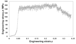
SIM images of the Cu-Ni-Si alloy micro-specimen before and after the tensile test are shown in Fig. 3(a) and (b), respectively. Numerous slip lines extended in the same direction were observed on the upper part of the specimen surface. The slip lines in the same direction indicate the specimen deformed by the dislocations activated on the single slip plane. The engineering stress-strain curves of the Cu-Ni-Si alloy micro-specimen and the bulk counterpart are shown in Fig. 4. The stress-strain curve of the micro-specimen shows the typical serrations and a decrease in the flow stress caused by the necking. Yield stress of the Cu-Ni-Si alloy obtained from the micro-tensile test is lower than that from the bulk tensile test. The SIM image, Fig. 3(a), shows that the micro-specimen is composed of only two grains, defined as grain α for the upper grain and grain β for the bottom grain. Figure 3(b) shows the deformation occurred only in the grain α by single slip. Thus, the strengthening by grain boundary did not occur, which led to the decrease in the strength21).

Figure 5 shows a SIM image and an EBSD mapping of cross-section of the Cu-Ni-Si alloy after the tensile test. In the EBSD image, the colors represent the crystal orientation against the loading direction. In the tensile test, the loading direction was corresponded to the crystal orientations of [727] in the grain α and $[9\bar{8}15]$ in the grain β. Tables 1 and 2 show Schmid factors of all the slip systems in fcc metals {111}<110> in the grain α and β. The maximum value of the Schmid factor is 0.43 for the grain α and 0.40 for the grain β. The results indicate that the deformation would accumulate in the grain α, which is in good agreement with the fact that the maximum Schmid factor of the grain α is larger than that of the grain β. Moreover, the slip trace of the grain α matched well with the $(1\bar{1}1)$ slip plane, which has the maximum Schmid factor. In Fig. 6, the magnified SEM image of side-view of the deformed micro-specimen shows the slip lines have similar angles of about 40° at the left side and 70° at the right side while traces of $(1\bar{1}1)$ plane is 42.5° at the left side and 70° at the right side. The results indicate that a large number of dislocations on $(1\bar{1}1)$ plane were moved to shear the tensile specimen leading to the necking in the grain α. From the EBSD image, Fig. 5(b), a gradual rotation of the crystal orientation in the grain α from [727] toward <110> is observed at the necking. Heavy deformation by sliding single slip system resulted the grain rotation to the slip direction activated during the tensile test.

Table 1
Calculated Schmid factors for
$\{111\}{<}11\bar{0}{>}$ slip systems of the top grain α.
| Slip plane |
Slip direction |
Schmid factors |
| $(111)$ |
$[\bar{1}10]$ |
0.30 |
| $[01\bar{1}]$ |
0.31 |
| $[10\bar{1}]$ |
0.01 |
| $(\bar{1}11)$ |
$[110]$ |
0.09 |
| $[101]$ |
0.13 |
| $[01\bar{1}]$ |
0.04 |
| $(1\bar{1}1)$ |
$[011]$ |
0.43 |
| $[110]$ |
0.43 |
| $[10\bar{1}]$ |
0.00 |
| $(11\bar{1})$ |
$[011]$ |
0.08 |
| $[\bar{1}10]$ |
0.04 |
| $[101]$ |
0.12 |
Table 2
Calculated Schmid factors for
$\{111\}{<}11\bar{0}{>}$ slip systems of the bottom grain β.
| Slip plane |
Slip direction |
Schmid factors |
| $(111)$ |
$[\bar{1}10]$ |
0.30 |
| $[01\bar{1}]$ |
0.40 |
| $[10\bar{1}]$ |
0.10 |
| $(\bar{1}11)$ |
$[110]$ |
0.00 |
| $[101]$ |
0.06 |
| $[01\bar{1}]$ |
0.05 |
| $(1\bar{1}1)$ |
$[011]$ |
0.24 |
| $[110]$ |
0.03 |
| $[10\bar{1}]$ |
0.21 |
| $(11\bar{1})$ |
$[011]$ |
0.11 |
| $[\bar{1}10]$ |
0.27 |
| $[101]$ |
0.37 |

Figure 7 shows work results of the hardening behavior obtained by the micro-tensile tests of (a) the pure Cu and (b) the Cu-Ni-Si alloy. At early stage of plastic deformation in the micro-tensile tests, the effect of the necking should be low, and this allows evaluation of the work hardening behavior. Right after the yielding, dislocations can easily glide on the slip plane with highest Schmid factor on both pure Cu and Cu-Ni-Si alloy. However, the Cu-Ni-Si alloy showed a notable work hardening when compared to the pure copper. In the Cu-Ni-Si alloy, δ-Ni2Si is the main precipitate contributing to the mechanical properties. The precipitates are reported to have formed in a shape of disk lying on {110} planes and are not shearable by dislocations, thus, they work as strong obstacles against the dislocation motion17). Non-shearable obstacles facilitate the dislocation multiplication by Orowan mechanism, which may lead to the enhanced work hardening in the Cu-Ni-Si alloy when compared to the pure Cu. Notable work hardening even in the easy glide regime, in which the dislocation moves on a single slip in the region of single crystal. This can be understood as the interaction of dislocations to the precipitates.

4. Conclusions
Micro-tensile tests of a pure copper and a Cu-Ni-Si alloy were conducted with micro-tensile specimens fabricated by FIB. In the micro-tensile tests, both the specimens showed characteristic large serrations during deformation, which were not observed in the bulk samples, and the obvious necking deformation, which caused a decrease in the flow stress. The micro-specimens of the pure copper and the Cu-Ni-Si alloy showed lower yield stresses than the bulk samples because of the absence of grain boundary. The EBSD analysis on the Cu-Ni-Si alloy specimen showed a gradual rotation of the crystal orientation in the deformed grain from the tensile axis [727] to the slip direction <110>. A notable work hardening behavior soon after yielding was observed in the Cu-Ni-Si alloy micro-specimen, which indicates the precipitates did work as strong obstacles against the dislocation motion even in the micro-scale sample.
Acknowledgments
This work has been supported by the Grant-in-Aid for Scientific Research (S) (JSPS KAKENHI Grant number 26220907) and CREST Project by the Japan Science and Technology Agency.
REFERENCES
- 1) H. Bei, S. Shim, G.M. Pharr and E.P. George: Appl. Phys. Lett. 91 (2007) 111915. 10.1063/1.2784948
- 2) E. Lilleodden: Scr. Mater. 62 (2010) 532–535. 10.1016/j.scriptamat.2009.12.048
- 3) T. Nagoshi, M. Mutoh, T.F.M. Chang, T. Sato and M. Sone: Mater. Lett. 117 (2014) 256–259. 10.1016/j.matlet.2013.12.017
- 4) D. Jang and J.R. Greer: Scr. Mater. 64 (2011) 77–80. 10.1016/j.scriptamat.2010.09.010
- 5) M.D. Uchic, D.M. Dimiduk, J.N. Florando and W.D. Nix: Science 305 (2004) 986–989. 10.1126/science.1098993
- 6) C. Motz, T. Schöberl and R. Pippan: Acta Mater. 53 (2005) 4269–4279. 10.1016/j.actamat.2005.05.036
- 7) H. Imamura, T. Nagoshi, A. Yoshida, T.F.M. Chang, S. Onaka and M. Sone: Microelectron. Eng. 100 (2012) 25–27. 10.1016/j.mee.2012.07.118
- 8) M.D. Uchic and D.A. Dimiduk: Mater. Sci. Eng. A 400–401 (2005) 268–278. 10.1016/j.msea.2005.03.082
- 9) J.R. Greer, W.C. Oliver and W.D. Nix: Acta Mater. 53 (2005) 1821–1830. 10.1016/j.actamat.2004.12.031
- 10) O. Kraft, P.A. Gruber, R. Mönig and D. Weygand: Annu. Rev. Mater. Res. 40 (2010) 293–317. 10.1146/annurev-matsci-082908-145409
- 11) M. Mutoh, T. Nagoshi, T.F.M. Chang, T. Sato and M. Sone: Microelectron. Eng. 111 (2013) 118–121. 10.1016/j.mee.2013.02.040
- 12) D. Kiener, W. Grosinger, G. Dehm and R. Pippan: Acta Mater. 56 (2008) 580–592. 10.1016/j.actamat.2007.10.015
- 13) J.Y. Kim and J.R. Greer: Acta Mater. 57 (2009) 5245–5253. 10.1016/j.actamat.2009.07.027
- 14) Y. Kihara, T. Nagoshi, T.F.M. Chang, H. Hosoda, T. Sato and M. Sone: Microelectron. Eng. 141 (2015) 17–20. 10.1016/j.mee.2015.01.001
- 15) Y. Kihara, T. Nagoshi, T.F.M. Chang, H. Hosoda, S. Tatsuo and M. Sone: Mater. Lett. 153 (2015) 36–39. 10.1016/j.matlet.2015.03.119
- 16) A. Araki, W.J. Poole, E. Kobayashi and T. Sato: Mater. Trans. 55 (2014) 501–505 10.2320/matertrans.MBW201326
- 17) A. Araki: Doctoral Thesis, Tokyo Institute of Technology, (2015).
- 18) G.P. Zhang, K. Takashima and Y. Higo: Mater. Sci. Eng. A 426 (2006) 95–100. 10.1016/j.msea.2006.03.090
- 19) R.P. Carreker Jr. and W.R. Hibbard Jr.: Acta Metall. 1 (1953) 654. 10.1016/0001-6160(53)90022-4
- 20) F. Sui and R. Sandström: Mater. Sci. Eng. A 663 (2016) 108–115. 10.1016/j.msea.2016.03.111
- 21) P.J. Imrich, C. Kirchlechner, C. Motz and G. Dehm: Acta Mater. 73 (2014) 240–250. 10.1016/j.actamat.2014.04.022