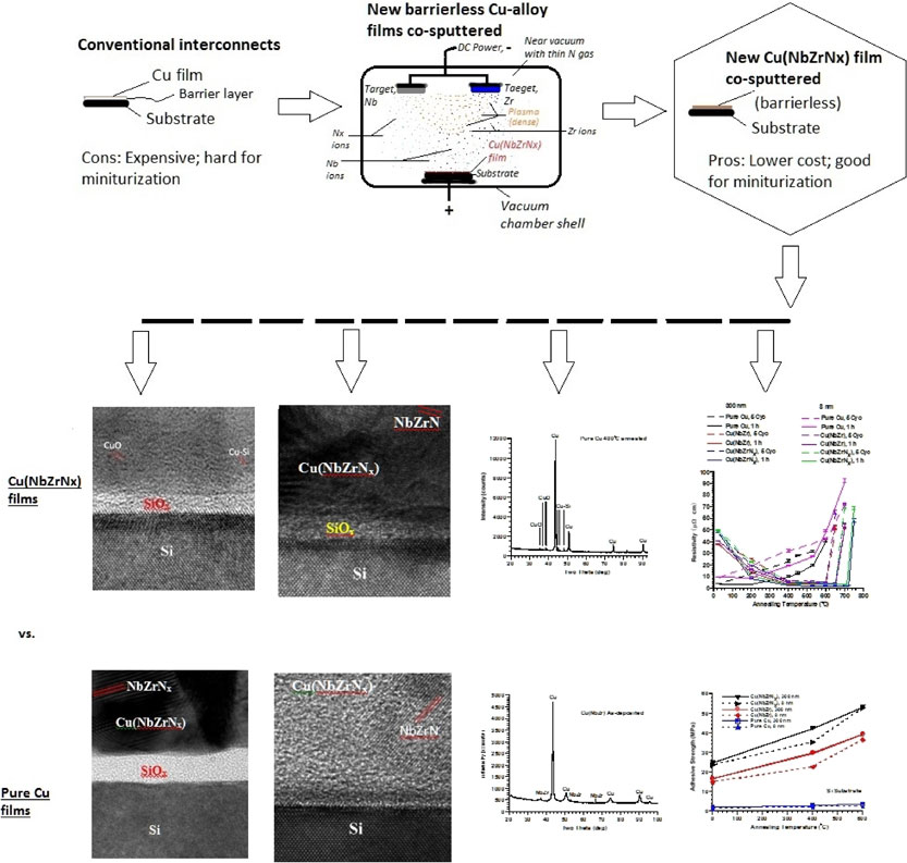
Abstract
Copper (Cu) alloy thin films deposited on barrierless substrates via sputtering and annealing processes have been essential for numerous microelectronic products and continue to be so in the new nanometer-range manufacture era. The search for better new films thus is crucial for further technical and manufacture advancement. The requirements on the new films lie in their stability in existence under high-temperature manufacture environments, low electric resistivity, less leakage current under various electric fields, and sufficient adhesion strength. For the search and advancement, I have developed a new type of films by co-sputtering impurities of niobium, Nb, and zirconium, Zr, with Cu within a vacuum chamber without any gas or with nitrogen (N) under low pressure, resulting in new Cu(NbZr) or Cu(NbZrNx) films whose fabrication processes and test results are detailed herein. The new type of films displays good physical features and seems desirable for microelectronic manufacture and to material science, too.