Abstract
Copper (Cu) alloy thin films deposited on barrierless substrates via sputtering and annealing processes have been essential for numerous microelectronic products and continue to be so in the new nanometer-range manufacture era. The search for better new films thus is crucial for further technical and manufacture advancement. The requirements on the new films lie in their stability in existence under high-temperature manufacture environments, low electric resistivity, less leakage current under various electric fields, and sufficient adhesion strength. For the search and advancement, I have developed a new type of films by co-sputtering impurities of niobium, Nb, and zirconium, Zr, with Cu within a vacuum chamber without any gas or with nitrogen (N) under low pressure, resulting in new Cu(NbZr) or Cu(NbZrNx) films whose fabrication processes and test results are detailed herein. The new type of films displays good physical features and seems desirable for microelectronic manufacture and to material science, too.

1. Introduction
For microelectronic interconnects, aluminum (Al) is often adopted over Cu for being less expensive, easier in deposition, and greater in adhesion; however, in contrast, Cu possesses higher electric conductivity, fewer hillocks rendering fewer shorts between interconnection levels, and greater resistance to electromigration, an effect that often breaks interconnects and causes failures of high-density ICs. Hence, Cu has gradually replaced Al in widespread industrial applications, particularly in ultra-large-scale integration (ULSI) manufacture using Cu metallization methods.1,2) Conversely, Cu is prone to diffusing into Si or SiO2 substrates resulting in Cu silicides, e.g., Cu3Si particles, which are detrimental to silicon and can catalyze silicon’s oxidation at room temperature.3) This is a major setback of Cu metallization. Conventionally, a barrier layer is inserted between Cu and Si substrates to separate the two and avert the Cu diffusion. However, when the barrier layer enters the nanometer range for device miniaturization, electron-grain boundary scattering can occur and cause resistivity increase.4) From the present study and my previous publications in this field, I have witnessed that using the Cu metallization technique by mixing Cu with materials immiscible to Cu via a plasma process, viz. a barrier metallization process, we can— if the immiscible materials are properly chosen with a correct, or good, composition combination— create a new type of Cu alloy films, e.g. Cu(TiBNx)5) and Cu(AuTiNx),6) which shall be able to fulfill the same barrier-layer-inserted objectives without the barrier layer and thus solving the mentioned problems associated with the inserted barrier layer. The new films created thus must imperatively retain high stability in existence under various high-temperature manufacturing environments where the films are to be processed and/or utilized.7)
In applying flip-chip technology— which uses bumps instead of gold wires to connect the chips— to popular electronic devices, such as cell phones, automotive parts, liquid crystal display (LCD)-driven IC products, high-level computer equipment, communication products, and the like that require a continuous reduction in area, height, and weight and/or withstanding harsh temperature, humidity, vibration, and even electromagnetic interference, and/or high-level performance, input-output (I/O) density, and cooling, and/or high I/O value and signal transmission quality, Cu, as traditionally chosen, must retain stability in existence under high temperatures and solderability to serve as a valid diffusion barrier and wetting layer8) in controlled collapse chip connection, which often seems quite challenging to pure Cu. Some alloy films,9–11) hence, have been developed for this issue. In the present study, a new type of Cu alloy films is further developed to meet the mentioned requirements and challenges.
For the wafer-level chip-scale packaging (WLCSP) method utilized in many electronic components, the demands on lead-free solder bumps have risen accordingly. The bumps are normally deposited by a plasma-related or electroplating technique, which partly constitutes under bump metallurgy (UBM). UBM ensures solder wettability, creates a diffusion barrier between a pad and a solder and provides sufficient adhesion and adequate electrical conductivity.12)
The barrierless metallization described herein not only simplifies manufacturing processes for electronic components and devices to reduce their manufacture cost but also renders a new methodology for creating new types of Cu alloy films, e.g. Cu(TiBNx)5) and Cu(AuTiNx),6) that exhibit unique micro-composition and good high-temperature quality, such as stability in existence under high temperatures. The methodology described herein shall be a refreshing contribution to the advancement of electronic manufacturing technology; besides, it can shed a light on material science. From Refs. 13)–16) that I was solely or deeply involved with in the past studies, we observe that the thermal stability— i.e. remaining in physical existence at high temperatures— of Cu(RuNx) alloy films reaches 680°C,13) and that of Cu(RuHfNx)14) and Cu(NbCNx)15) 720°C, which is quite impressive comparing to that of pure Cu, merely 200°C. On the resistivity issue, the resistivity of Cu(AgNx) films16) reaches 2.2 µΩ cm after annealing at 600°C.
From Ref. 17), we observe that Nb–Zr holds the diffusion barrier characteristic. Nb has a melting point of 2477°C and Zr 1855°C. The two elements are, hence, adopted in the study to try creating a new type of alloy films, viz. Cu(NbZrNx), the thermal stability of which is found sustainable up to 720°C. The new films can simplify the manufacturing process and seem useful for some industrial usage, such as barrierless metallization on, e.g., Si substrates, wetting and diffusion barrier layers for solder joints, and better Cu alloy seed layers in flip-chip technology, potential materials for medical care needs,18) and so on.
2. Experimental Procedure
The new Cu(NbZrNx) films are made into two thicknesses, i.e. 300 nm and 8 nm, containing 0.4 at% Nb and 0.3 at% Zr in the final optimal or nearly optimal composition format, which is thus adopted and investigated throughout the present study. During the search of an optimal or nearly optimal Cu(NbZrNx) film, the element amounts of co-sputtered Nb, Zr, and N were repeatedly adjusted, via either adding or subtracting each amount of the elements for various trial composition combinations, then the resulted films were annealed at 400°C and tested and measured afterward— all other composition combinations were observed with less optimal performances than the one mentioned above.
The new films are created using plasma technology by co-sputtering Cu, Nb, Zr in a vacuum chamber with N2 gas and followed by vacuum isothermal annealing at 200, 400, 530, or 750°C for 1 h at each temperature. The crystal structures and microstructures of the films before and after annealing were analyzed using X-ray diffraction (XRD), X-ray photoelectron spectroscopy, focused ion beam microscopy, transmission electron microscopy (TEM), and X-ray energy-dispersive spectroscopy. Further, the film resistivity was measured at room temperature using a four-point probe, and leakage current characteristics were determined based on the current-voltage curves of the films deposited on SiO2/Si substrates, forming typical metal–oxide–semiconductor (MOS) capacitors with the other pure Cu layer deposited on the other side of the substrates. The electric reliability of the Cu films was determined from their time-dependent dielectric-breakdown (TDDB) lifetime. A cyclic annealing process was executed as follows: The vacuum pressure was set at 10−7 Torr and the temperature was increased from room temperature to 200–720°C. Five cycles, which took approximately 57.9 h in total duration, were implemented without a holding temperature, and the heating and cooling rates during each cycle were 6.7 and 10°C/min, respectively.
The adhesion property of the films was evaluated by measuring their pull-off strength according to ASTM International standard D4541-02.27. An Sn layer is thermally evaporated atop the new Cu(NbZrNx) film to achieve a stable flip-chip solder joint. The thermal evaporation, driven by 220 Vac, 200–230 A, power supply, starts when the vacuum reaches ∼3 × 10⁻⁶ Torr and lasts for ∼5 h to produce a 2.7-µm-thick Sn layer.
3. Results and Discussion
Figures 1(a) and (b) show the XRD diffraction patterns for as-deposited Cu(NbZrNx) and Cu(NbZr) films respectively. The patterns display the existence of the NbZrNx phase (JCPDS 89-5137) and NbZr phase (JCPDS 65-9440), while there is no phase shift between the two Cu peaks of intensity. No reaction compounds are found between Cu and Nb or between Cu and Zr— namely, no interactions between Cu and Nb and between Cu and Zr are detected.
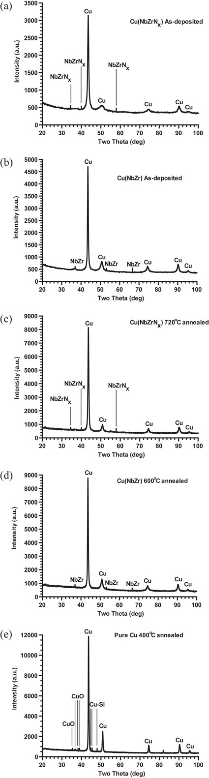
Figures 1(c) and (d) show the XRD diffraction pattern for Cu(NbZrNx) and Cu(NbZr) films after they are annealed at 720 and 600°C, respectively. The patterns display that Nb, Zr, and N together and Nb and Zr are still solidly dissolved in the Cu(NbZrNx) and Cu(NbZr) films, respectively, verifying that the new films retain high thermal stability. In comparison, Fig. 1(e) indicates that a pure Cu film forms CuO and Cu–Si compounds induced by oxidation during a 400°C annealing process. This confirms that the formation of Cu(NbZrNx) and Cu(NbZr) phases dissolved in pure Cu can raise the new films’ and Cu(NbZr) films’ high-temperature stability to 720 and 600°C, respectively.
Figures 2(a) and (b) show the line scan diagrams of pure Cu films having been annealed at 400°C and Cu(NbZrNx) films having been annealed at 720°C. The pure Cu films’ line scan diagram confirms that oxidation has occurred, which is also registered as CuO and Cu–Si compounds displayed in Fig. 1(e). No oxidation takes place within the Cu(NbZrNx) films, representing their stability at high temperature, which probably is owing to the formed NbZrNx compound solidly dissolved in the new films. This conforms with the XRD pattern shown in Fig. 1(c), too.

Figure 3(a) represents the cross-sectional transmission electron microscopy (TEM) image of pure Cu films after annealing at 400°C. From Fig. 3(b), a magnified image of Fig. 3(a), we observe oxides CuO and Cu–Si owing to oxidation, which confirms with the XRD pattern shown in Fig. 1(e) and the line scan diagram shown in Fig. 2(a). Figure 3(c) exhibits the cross-sectional image of Cu(NbZrNx) films after annealing at 720°C. From Fig. 3(d), a magnified version of Fig. 3(c), we observe a 2.59 Å d-spacing NbZrNx phase (JCPDS89-5137) solidly dissolved in the new films, which elevates the films’ stability at high temperatures. After the annealing, the grain size grows up to 52 ± 3 nm which suppresses the interaction between the Cu and Si, averting oxidation. The result confirms the XRD pattern of Fig. 1(c) and the line scan diagram of Fig. 2(b).

The films are placed in a vacuum with various temperatures of 200 to 750°C and annealed for either five (5) cyclic-annealing cycles or isothermal annealing for 1 h. For the new 300 nm-thick Cu(NbZrNx) films, the film resistivity reduced, from earlier as-deposited 2.63 µΩ cm to 2.21 µΩ cm after annealing at 720°C for 1 h, as shown in Fig. 4(a). The isothermal annealing process renders better resistivity performance than its cyclic counterpart, as observed from Fig. 4(a). The resistivity values of the new Cu(NbZrNx) films further drop to 2.07 and 2.03 µΩ cm after they have been annealed at 400 and 450°C, respectively, for slightly over 240 h, as shown in Fig. 4(b), revealing the new alloy films’ anti-oxidation stability at 400 and 450°C. For comparison, the same annealing processes were applied to Cu(NbZr) films and their behaviors are also included in Fig. 4(b), which indicates that the newly-developed Cu(NbZrNx) films are to some extent better than Cu(NbZr) films in resistivity performance— the lower, the better— once their annealing time length, at 400 and 450°C, is over approximately 0.9 h.

To inspect the Cu depth profile, we first applied nitric acid to remove the surface layer of the pure Cu and the new alloy films then measured their Cu diffusion depth using secondary-ion mass spectrometry (SIMS). Figure 5 displays the depth profiles of Cu, Cu(NbZr), and Cu(NbZrNx) films after annealing at 400°C, wherein we observe the Cu diffusion depth of Cu(NbZrNx) films is shallower than that of Cu(NbZr) films. This further confirms that the stability of Cu(NbZrNx) films at high temperatures is better than that of Cu(NbZr). Since resistivity and Cu diffusion depth are two key factors in industrial application, the former is hence determined to be superior to the latter in this aspect.

Figure 6(a) shows the MOS capacitors I–V curves after the pure Cu, Cu(NbZr), and Cu(NbZrNx) films were deposited on SiO2/Si substrates and annealed at 400°C for 1 h. The annealing temperature is set at 400°C for the general high-temperature stability evaluation.19) When an electric field exceeds 2.7 MV/cm, the apparent Cu diffusion into SiO2 will result in the increase of leakage current in the Cu gates of the MOS capacitors. At 2 MV/cm, the leakage current of the Cu(NbZrNx) films is 1.35 × 10⁻¹³ A/cm2, far lower than that of Cu(NbZr) (1.43 × 10⁻¹⁰ A/cm2), Cu(RuNx)13) (3.17 × 10⁻¹⁰ A/cm2), Cu(RuHfNx)14) (1.83 × 10⁻¹⁰ A/cm2) and pure Cu (1.6 × 10⁻⁷ A/cm2).11) This reveals that the new alloy films retain good stability under a high electric field, which is in alignment with the diffusion depth result tested by SIMS shown in Fig. 5. Figure 6(b) displays the I-V curves of three types of capacitors stressed at 2.7 MV/cm. As time goes by, the ion density and electric charges captured and cumulated at the oxidized layer will reach a threshold and cause an abrupt increase in leakage current, resulting in structural damage. The time that the leakage current abruptly increases is defined as the failure time. For pure Cu, Cu(NbZr), and Cu(NbZrNx) films, the time durations for the Cu ion density to reach the threshold are, respectively, 1,000, 222,800, and 322,000 s; upon that time, a current conduction path will be formed between the anode and the cathode and damage their capacitor structure. At 2.7 MV/cm, the time to reach the structure damage for Cu(NbZrNx) films is substantially longer than that for pure Cu, by 322 times, and that for Cu(NbZr), by 44.5% margin, indicating the superior electrical reliability of the new films. Figure 6(c) shows the relationships of TDDB lifetime of pure Cu, Cu(NbZr), and Cu(NbZrNx) films for various electric field strength. From Fig. 6(c), we observe that the TDDB lifetime for the new films under approximately 2.45 MV/cm or less can satisfy 10-year projected reliability, while the TDDB lifetime of Cu(NbZrNx) films under 3.5 MV/cm, or less, electric stress is longer than that of Cu(NbZr) and pure Cu. This is consistent with the new films’ better diffusion-barrier layer and thermal stability over TiN,20) Ta,20) and TaN.20)

Heretofore, the above text has mainly dealt with interconnects using the new alloy films. Next, we will deal with chip-packaging issues by inserting the new Cu(NbZrNx) alloy film between Si and Sn layers to reduce the prior Cu–Sn interaction and to suppress the prior formation of intermetallic compounds (IMCs) often incurred at the metallic interface in the chip-packaging process.
Figure 7(a) exhibits the XRD pattern of as-deposited Sn/Cu(NbZrNx)/Si structure, while Fig. 7(b) shows the XRD pattern of Sn/Cu(NbZrNx)/Si structure after aging for 8 days. Although some Cu–Sn intermetallic compounds are formed, the Cu(NbZrNx) as a buffer layer remains intact without interacting with Sn, confirming the stability of Cu(NbZrNx). In comparison, the pure Cu has vanished by turning into Cu–Sn metallic compounds after 8 days’ aging as shown in the XRD result of Fig. 7(c). It is or is highly likely, via comparison of Figs. 7(b) and 7(c) and my deduction, that the NbZrNx compound within the new Cu(NbZrNx) films is solely or mainly responsible for the improvement of the new films’ stability during the aging period.

Figures 8(a)–(c) are the cross-sectional TEM images of as-deposited Sn/Cu(NbZrNx)/Si structure, and Figs. 8(d)–(f) that of the same structure after aging for 8 days at 200°C, while Figs. 8(c) and (f) are the magnification of Figs. 8(b) and (e), respectively. Figures 8(c) and 8(f) reveal that before and after annealing, an NbZrNx phase of 2.59 Å d-spacing exists in the new alloy film, which conforms with the XRD patterns shown in Figs. 1(a) and 1(c). This again verifies the Cu(NbZrNx) buffer’s high stability in existence and high capability in suppressing the interaction between the Cu and Sn.

Figure 9(a) shows that the thickness of the new films’ IMC before and after annealing is smaller than that of Cu(NbZr) and pure Cu. From Fig. 9(b), we observe that after 8 day’s aging, the Cu(NbZrNx) layer remains 140-nm thick, and the Cu(NbZr) layer 64-nm thick, while the pure Cu layer vanishes completely and disappears after approximately 48 h. This suggests that Cu(NbZrNx) is a very stable material. The addition of 3–4 at% of an alloy to Cu to inhibit the formation of intermetallic compounds at the interface, as proposed and achieved in the present study, has not been reported in the literature. The exact mechanism of this phenomenon is still unclear; further study is needed to understand this discovery.

Figure 10 shows the results of ASTM D4541-02 adhesion tests for 8- and 300-nm-thick pure Cu, Cu(NbZr), and Cu(NbZrNx) films before and after annealing at various temperatures up to 600°C for 1 h. All alloy films, be they 8- or 300-nm thick, show their adhesion strength superior to that of their pure Cu counterpart before, i.e. as-deposited, and after annealing at various temperatures. The adhesion strength of the 300-nm-thick new films registers 24.8 ± 0.02 MPa, the highest, and is greater than that of its pure counterpart by 11–12 times, as shown in Fig. 10. After annealing at 600°C, the adhesion strength of the new Cu(NbZrNx) films raises to 53.2 ± 0.01 MPa, far greater than that of the pure Cu films, merely 3.7 ± 0.02 MPa— that is 14–15 times greater. This is similar to the prior adhesion test results for Cu(RuNx).13) The much greater adhesion strength rendered by the new films over their pure Cu counterpart in the study seems to be caused by the NbZrNx compound segregated at the film-substrate interface, which still needs further study to conclude or confirm.

4. Conclusion
In the study, a new type of Cu(NbZrNx) alloy films appears to possess great stability in existence under high temperatures, low resistivity, low leakage current when used in MOS capacitors, long TDDB lifetime duration which meets 10-year projected reliability at electric stress of 2.45 MV/cm or less, and great adhesion strength which is 14–15 times greater than that of its pure Cu counterpart. With their low resistivity, good electric stability under high electric fields, and good TDDB lifetime performance, they seem to be a good candidate material for both barrierless layer and interconnect applications needed in, e.g., microelectronic manufacture and circuit printing industries.
The new Cu(NbZrNx) alloy films can also be used as a valid diffusion barrier and wetting layer in the flip-chip manufacturing method and as a diffusion barrier between a pad and a solder, rendering sufficient adhesion and adequate electrical conductivity, for UBM associated with WLCSP method adopted in manufacturing many electronic components. The barrierless metallization described herein not only simplifies manufacturing processes for electronic components and devices to reduce their manufacturing cost but also can render new types of Cu alloy films by mixing mutually-immiscible materials. The study renders a refreshing contribution to the advancement of manufacturing technology and shall shed a light on material science, too.
Acknowledgment
This work was sponsored by the National Science Council of the Republic of China in Taiwan, under Project No. 106-2221-E-243-001-MY3-. The author would also like to thank the invaluable assistance of Dr. John Yanhao Chen, Director of eWay Inc.'s eWay Translation & Writing Services Division in Taiwan.
REFERENCES
- 1) S.K. Kang, D.Y. Shih, K. Fogel, P. Lauro, M.J. Yim, G.G. Advocate, M. Griffin, C. Goldsmith, D.W. Henderson, T.A. Gosselin, D.E. King, J.J. Konrad, A. Sarkhel and K.J. Puttlitz: IEEE Trans. Electron. Packag. Manuf. 25 (2002) 155–161. doi:10.1109/TEPM.2002.801165
- 2) C.E. Ho, S.C. Yang and C.R. Kao: J. Mater. Sci. Mater. Electron. 18 (2007) 155–174. doi:10.1007/s10854-006-9031-5
- 3) L. Stolt, A. Charai, F.M. D’Heurle, P.M. Fryer and J.M.E. Harper: J. Vac. Sci. Technol. A 9 (1991) 1501–1505. doi:10.1116/1.577653
- 4) J.G. Lozano, S. Lozano-Perez, J. Bogan, Y.C. Wang, B. Brennan, P.D. Nellist and G. Hughes: Appl. Phys. Lett. 98 (2011) 123112. doi:10.1063/1.3569146
- 5) C.H. Lin: Jpn. J. Appl. Phys. 55 (2016) 06JD02. doi:10.7567/JJAP.55.06JD02
- 6) C.H. Lin: Jpn. J. Appl. Phys. 55 (2016) 01AA13. doi:10.7567/JJAP.55.01AA13
- 7) J.-K. Koo and J.-H. Lee: Mater. Trans. 58 (2017) 148–151. doi:10.2320/matertrans.MA201606
- 8) C.H. Lin: Jpn. J. Appl. Phys. 52 (2013) 05FB01. doi:10.7567/JJAP.52.05FB01
- 9) C.H. Lin, H.Y. Chuang and C.R. Kao: Jpn. J. Appl. Phys. 52 (2013) 01AC12. doi:10.7567/JJAP.52.01AC12
- 10) H.Y. Chuang, C.H. Lin, J.P. Chu and C.R. Kao: J. Alloy. Compd. 504 (2010) L25–L27. doi:10.1016/j.jallcom.2010.05.131
- 11) C.H. Lin, J.P. Chu, T. Mahalingam, T.N. Lin and S.F. Wang: J. Mater. Res. 18 (2003) 14. doi:10.1557/JMR.2003.0196
- 12) S.M. Rossnagel and T.S. Kuan: J. Vac. Sci. Technol. B 22 (2004) 240–247. doi:10.1116/1.1642639
- 13) J.P. Chu, C.H. Lin and V.S. John: Appl. Phys. Lett. 91 (2007) 132109. doi:10.1063/1.2790843
- 14) C.H. Lin, W.K. Leau and C.H. Wu: Electron. Mater. 39 (2010) 2441–2447. doi:10.1007/s11664-010-1300-7
- 15) C.H. Lin: Microelectron. Eng. 223 (2020) 111217. doi:10.1016/j.mee.2020.111217
- 16) C.H. Lin and W.K. Leau: Electron. Mater. 38 (2009) 2212–2221. doi:10.1007/s11664-009-0904-2
- 17) H. Skliarova, O. Azzolini, R.R. Johnson and V. Palmieri: J. Alloy. Compd. 639 (2015) 488–495. doi:10.1016/j.jallcom.2015.03.181
- 18) C.H. Lin: Bull. Mater. Sci. 43 (2020) 1. doi:10.1007/s12034-019-1971-5
- 19) K. Barmak, C. Cabral, Jr., K.P. Rodbell and J.M.E. Harper: J. Vac. Sci. Technol. B 24 (2006) 2485–2498. doi:10.1116/1.2357744
- 20) G. Soto, A. Rosas, M.H. Farias, W. De la Cruz and J.A. Diaz: Mater. Charact. 58 (2007) 519–526. doi:10.1016/j.matchar.2006.06.025