3. Results and Discussions
The effects of annealing temperature and time on the melted mark of copper wire are examined, which includes surface morphology observation, oxide phase identification and crystallite size calculation, parabolic rate constant and activation calculation, and microstructure characterization.
3.1 Surface morphology observation
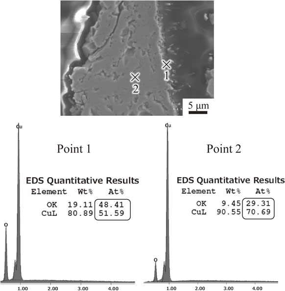
Initially, the effect of annealing temperature on the surface morphology evolution of melted marks on copper wire was examined. Figure 1 shows the surface micrographs of melted marks on copper wire annealed for two hours at temperatures of (a) 1000°C, (b) 800°C, (c) 600°C, (d) 400°C and (e) 220°C. At 1000°C, the middle of the oxide grains displayed a dark depression surrounded by strong ridges at their grain boundaries in the bright region. The elemental analysis by EDS was conducted both in the middle of the oxide grain at point 1 and at the grain boundary at point 2. The presence of copper and oxygen elements of 1:1, equivalent to the amount of copper and oxygen in CuO, is indicated by the EDS spectrum in the bright region at point 1. In the middle of the oxide grain (point 2), meanwhile, the amount of copper and oxygen at their grain boundary is about comparable to the theoretical copper and oxygen percentages in Cu2O. Accordingly, the presence of Cu2O grains enclosed by the CuO at the grain boundary is the typical morphology of melted marks after heat treatment at 1000°C.

At 800°C, oxide grains are smaller than at 1000°C, with the CuO scale uniformly covered on the outer surface. With decreasing the temperature to 600°C, the EDS results of the cross-section of the melted mark in Fig. 2 reveal the existence of Cu2O at the inner surface (point 2) and CuO whiskers (point 1) randomly nucleated on the Cu2O surface. It has been reported that the CuO whiskers nucleated on Cu2O grow predominantly by surface diffusion resulting from the breakup of adsorbed oxygen due to the presence of water vapor.8–12) The surface at 220°C and 400°C is not flat with slight coverage by CuO, and whiskers cannot be observed at these temperatures. It can be seen that depending on the temperature, the morphology of copper oxide develops with distinct characteristics. The larger oxide grain structure is observed at surface of the melted mark annealed at 1000°C because the atoms transported at higher temperatures have enough diffusion activation energy to occupy the crystal lattice and induce the small grains by grain boundary diffusion, resulting in larger grains than when annealed at 800°C.16,17)
CuO whiskers are observed on Cu2O surface of melted marks annealed at 600°C in Fig. 1(c). The growth of whiskers could be supported by surface diffusion through the overgrowth at their tips from screw dislocation emerging on the metal surface due to the breakup of the absorbed oxygen.8,9) Furthermore, the tiny oxides was investigated even at low temperature of 220°C and 400°C as shown in Figs. 1(d) and 1(e). Although the Cu2O and CuO were identified via EDS, which may not be sufficient to conclude their existence, XRD has been used to confirm the presence of Cu2O and CuO in Section 3.2.
3.2 Oxide phase identification and crystallite size calculation
The phase identification of the oxide layer by XRD can be utilized to validate the existence of the copper oxide. The XRD patterns of the copper oxide surface on melted marks of copper wire annealed under 1000°C, 800°C, 600°C, 400°C, and 220°C for 2 hours and cooled down in the furnace are demonstrated in Fig. 3. The oxide surface on the specimen or the oxide peeled off from the specimen was analyzed. The peak positions of 29.42, 36.29, 42.16, 61.27, 73.40, and 77.27 degrees correspond to the (110), (111), (200), (220), (311), and (220) planes of Cu2O. These peaks match Cu2O powder from JCPDS file no. 00-002-1067, indicating that Cu2O is present at the surface of the melted mark for all annealing temperatures from 1000°C to 220°C. The oxidation is described by the reaction of copper atoms with oxygen atoms to generate Cu2O, which is written as the following reaction: 2Cu + 1/2 O2 → Cu2O.16) At 220°C, the copper oxide formed on the surface of the melted mark has an extremely low amount due to the low temperature, and all peaks of oxide layers including a base copper melted mark were very slightly detected. From 600°C to 400°C, the peak positions at 35.44, 38.58, 48.74, 58.21, 66.36, and 68.08 degrees correspond to the (002), (111), (-202), (202), (022), and (113) CuO planes. Each peak position is in good agreement with CuO powder from JCPDS file no. 00-002-1040 confirming the presence of CuO. The reaction between copper and oxygen can be described as follows: 2Cu2O + O2 → 4CuO.16) The growth of CuO on the Cu2O layer is extremely small at high temperatures because of low atomic transport due to the absence of vacancies in CuO for fast atomic transport.8) As a result, a small amount of CuO compared to Cu2O results in unnoticeable CuO in the XRD patterns at 1000°C. A little CuO at 1000°C is also consistent with the appearance of CuO at the only grain boundary of the oxide grains examined by EDS in Fig. 1(a). With decreasing annealing temperature to 800°C, the CuO phase starts to appear and the XRD pattern presents an extra small peak near 2θ = 33° which agrees well with the reflection from the (110) plane of CuO. Based on the XRD patterns at 600°C and 400°C, the oxide surface of the melted marks consists of a mixture between the Cu2O and CuO phases. The phase diagram suggests that CuO is the stable phase at lower temperatures. Therefore, the Cu2O slowly and finally oxidizes into the CuO phase,8,12,16) but may not entirely oxidize due to the low temperature.

The crystallite size of Cu2O was also estimated using the Debye-Scherrer formula:18–20)
| \begin{equation}
D = 0.9\lambda/\beta \cos\theta
\end{equation}
| (1) |
Here, D is crystallite diameter dimension, λ is X-Ray wavelength (0.1541 nm), β is FWHM (Full width at half maximum) and θ is the diffraction angle. The broadened major peak located at 2θ = 36.29 was used to determine the crystallite sizes of all specimens.
Figure 4 plots the Cu
2O crystallite size versus annealing temperature. The Cu
2O crystallite size increases with the annealing temperature from 30 nm to 47 nm at annealing temperatures between 400°C to 1000°C. Besides, the crystallite size at 220°C is differ from the straight line from 400 to 1000°C, which indicated that the driving force and growth rate could be different between temperatures below 400°C and above 400°C. Increasing the temperature can enhance the distance between planes of atoms resulting in Cu
2O crystallite forms becoming larger in size. It can be seen that estimating Cu
2O crystallite size from the XRD peak by using the Debye-Scherrer formula might support fire investigators in evaluating the fire temperature at the fire site. According to previous research, the calculated Cu
2O crystallite sizes at an annealing temperature of 1000°C under furnace, air, and water cooling were 50 nm, 46 nm, and 44 nm, respectively.
4) In comparison, the obtained crystallite size at the same temperature for this work is 47 nm which is similar to the previous work. However, the crystallite size reduces from 47 nm at 1000°C to 30 nm at 400°C. It is obvious that temperature changes have a greater effect on crystallite size than cooling rates.
3.3 Oxide layer thickness
The oxide layers were observed on the surface of the melted marks annealed at various times and temperatures, as depicted in Fig. 5. The specimen was cut perpendicular to the oxide layer passing through the center of the specimen, as much as possible. As discussed in the previous section, CuO is slightly formed on the Cu2O surface, so it cannot be observed with an optical microscope in the cross-section after mounting and polishing. Thus, measuring the CuO layer for each specimen is impossible, whereas the Cu2O layer clearly appears on the copper melted mark. As a result, Cu2O layers were measured for all heat treatment conditions. The variation of Cu2O layer thickness with annealing time at constant temperature is displayed in Fig. 5. In addition, specimens with a holding time of 0 hours are shown as reference microstructures for each temperature. An increase in annealing time mainly increases the thickness of Cu2O due to the longer time promoting more reaction between copper and oxygen to form Cu2O. Along with the increase of annealing temperature, the thickness of the Cu2O is rapidly increasing with temperature. At 220°C and 400°C, the Cu2O layer is very small because the generation of Cu2O is restrained due to the low temperature, then Cu2O slowly grows and gradually oxidizes into CuO. At an intermediate temperature range, the thickness of Cu2O increases, as copper cannot transfer to combine with oxygen at the copper/oxygen interface. Then, Cu2O become unstable and finally, fully oxidizes into CuO as exhibited in the SEM and XRD results. At 1000°C, the Cu2O layer with some porosities grows predominantly because of its thermodynamic stability and hardly oxidizes into CuO.17)

Furthermore, the linear relationships are observed between the average oxide layer thickness and the square root of time in Fig. 6, indicating that the oxidations at 1000°C, 800°C, 600°C, 400°C, and 220°C are controlled by a diffusional process.21) Moreover, Cu2O growth at 220°C to 1000°C obeys the parabolic rate law, which is consistent with reporting by Zhu et al.11) The parabolic rate constant (kp) or the diffusion rate constant can be calculated from the slope of the parabolic plot. The values are 20.4 µm2/s at 1000°C, 5.8 µm2/s at 800°C, 0.13 µm2/s at 600°C, 6.12 × 10⁻⁴ µm2/s at 400°C and 1 × 10⁻⁴ µm2/s at 220°C. These rates are controlled by the ability of the copper and oxygen atoms to migrate through the oxide layer and encounter each other. As the thickness increases, it takes longer for the copper and oxygen atoms to diffuse through, and so the oxidation is limited by the diffusion rate. Additionally, the parabolic rate constant at the low temperature of 220°C is similar to the rate of 1 × 10⁻⁴ um2/s as reported by Lee et al.21)

An increase in oxide layer thickness and faster oxidation rate is caused by increasing the processing temperature, as discussed previously. Therefore, the parabolic rate constant (kp) must be modifiable for temperature effects in order to describe oxidation using the parabolic approach. Accordingly, the Arrhenius expression in eq. (2) well describes the effects of temperature on the parabolic rate constant.22)
| \begin{equation}
k_{p} = A\,\mathit{exp} (-Q/RT)
\end{equation}
| (2) |
Where,
kp is the parabolic rate constant (µm
2/s),
Q is the activation energy (J),
R is the gas constant (8.314 J/mol K),
T is temperature (K) and
A is the pre-exponential constant (µm
2/s). The Arrhenius plot of the parabolic rate constants at 220°C to 1000°C for Cu
2O oxidation under atmosphere is shown in
Fig. 7. The Arrhenius plot is roughly divided into two regions; a high temperature region (400°C to 1000°C), and a low temperature region (220°C to 400°C). By calculation, the activation energy from the slope of log k
p vs. reciprocal-temperature plot of 127 kJ is obtained at the high temperature range. The calculated Q value of 28 kJ is achieved in the low temperature range (220°C to 400°C). Interestingly, the dependence on temperature closely resembles the results reported in the literature.
8–11) Tylecote
23) published Q values of 123 kJ and 39 kJ at temperature ranges of 600°C to 900°C and 300°C to 500°C, respectively. According to the agreement with the oxidation activation energy, it could be assumed that diffusion in the Cu
2O layer at a broader temperature range is the rate-determining step which is inferred to be the outward diffusion of copper atoms in Cu
2O.
8,12,24) In general, the oxidation between copper and oxygen occurs when copper is exposed to the atmosphere at high temperatures. In the melted mark specimens, for further oxidation, the oxidation continues according to whether the copper atoms of the melted mark diffuse outward through the oxide layer to combine with oxygen from the air or oxygen from the air diffuses inward to encounter the copper atoms of the melted mark.
22)
In detail, the rate of lattice, grain boundary, and surface diffusion is characterized by the diffusion coefficients related to activation energy Ql, Qgb, Qs where Ql > Qgb > Qs.25) It was thought that the oxidation in Cu2O over the wider range from 400°C to 1000°C with higher activation energy might have contributions from lattice diffusion. Meanwhile, lower activation energy may result in grain boundary diffusion, which contributes to copper oxidation at low temperatures of 220°C to 400°C.8,12) Additionally, because the activation energy for surface diffusion is lower than that for lattice diffusion, growth associated with screw dislocation steps will result in whisker growth at 600°C by surface diffusion. In contrast, as temperature rises, lateral lattice diffusion becomes more favorable, and oxide growth could result in flatter morphologies such as pyramids.25)
3.5 Microstructure characterization
The microstructural evolutions of melted marks on copper wire under various annealing temperatures and annealing times are demonstrated in Fig. 8. Due to the structure of the electric furnace, the heating rate varied from 0.4 to 0.9 K/s, so the specimen holding 0 hours was prepared as the reference structure for each holding temperature. It can be clearly seen that there is a difference in microstructural evolution from low temperatures to high temperatures. A dendritic structure in columnar grains can be seen at low temperatures (220°C to 600°C), but it gradually disappears at 800°C and 1000°C. The mechanism underlying the microstructural change is discussed as follows. Before heat treatment, the original microstructure of melted mark on copper wire comprises copper dendrites in columnar grains surrounded by the (Cu+Cu2O) eutectic structure.26,27) After heat treatment at 220°C to 400°C for different annealing times, the dendritic structures can be noticed for all annealing times due to low temperature, similar to the microstructure before heat treatment. However, the darker color on the copper dendrites gradually appears after annealing at 400°C for 4 and 8 hours. It was thought that small particles of Cu2O start to precipitate on the copper dendrites during the heat treatment process for a longer time.28) When increasing the temperature to 600°C, the dendritic structure is still observed for all annealing times. Additionally, more precipitated Cu2O particles on copper dendrites can be observed. It is interesting that the dendrites disappear after heat treatment for an annealing time of more than one hour at 800°C and for all annealing times at 1000°C. Dendrites can still be seen in unannealed specimens at 800°C, but they vanish after that. With the above discussion, the microstructure before heat treatment consists of the primary copper dendrites in a bright region inside columnar grains and the (Cu+Cu2O) eutectic phase in a dark region.

After heat treatment at high temperatures, copper dendrites in the bright region disappear completely because copper dendrites in the same crystallographic orientation must minimize their interfacial energy by dissolving and trying to connect to form a large grain over time. Meanwhile, the (Cu+Cu2O) eutectic phase is transformed into Cu2O particles that precipitate all over the copper matrix. Furthermore, the different colors separated by the grain boundary on the microstructure after annealing, for example, at 1000°C for 120 minutes, indicate different crystal orientations for each grain. Therefore, the columnar grain structure with precipitated Cu2O particles is the final microstructure of the melted mark after heat treatment at a high temperature range (800°C to 1000°C).
For that reason, the microstructural evolution under various heat treatment conditions might be used to describe the fire behaviors. In the case of high fire temperatures, the final structure should be the same as the microstructure after high-temperature annealing, with dendrites disappearing and columnar grains with precipitated Cu2O.
In summary, the characteristic feature after heat treatment at low temperatures (220°C to 600°C) is copper dendrites in columnar grains enclosed by the (Cu+Cu2O) eutectic under Cu2O layer and CuO. At high annealing temperatures (800°C to 1000°C), columnar grains with Cu2O precipitates under Cu2O layer become the typical microstructure.
In a real fire accident, oxygen gas or other gases may be released due to the combustion of materials in the fire. These gases may have an impact on the microstructure and copper oxide. Moreover, oxygen pressure in the real fire site may differ from this experiment. Because of various fire behaviors, this work could not comprehensively simulate all fire conditions. As a result, the oxygen effect on the melted mark of copper wire is expected to be studied in the future.


