特集「Society 5.0時代を創出する異種材料集積半導体デバイス」
ダイヤモンド高周波・パワーデバイス応用に向けた金属‐酸化膜‐半導体(MOS)界面の現状と課題
2021 年 64 巻 2 号 p. 80-85
詳細
2021 年 64 巻 2 号 p. 80-85
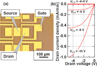
Diamond has various useful material properties such as a wide bandgap, high carrier mobility, high breakdown field, and high thermal conductivity. Therefore, diamond is expected as high-frequency, low-loss and high-power device materials. Our fabricated diamond metal-oxide-semiconductor field-effect transistors (MOSFETs) showed normally off properties, which is important for power devices. However, the MOSFETs suffer from low field-effect mobility, which is mainly attributed to existence of high interface state density near the valence band edge on diamond. In this report, we introduce the lateral growth technique and the OH termination technique. We also discuss electrical properties of diamond MOSFETs and MOS capacitors.