e-Journal of Surface Science and Nanotechnology
Online ISSN : 1348-0391
ISSN-L : 1348-0391
Volume 23, Issue 2
Displaying 1-16 of 16 articles from this issue
Regular Papers
  • Yodai Kobayashi, Kenji Ohoyama, Shoichi Uechi, Koji Kimura, Naohisa Ha ...
    Article type: Regular Paper
    Subject area: Structure
    2025Volume 23Issue 2 Pages 92-96
    Published: April 05, 2025
    Released on J-STAGE: May 31, 2025
    Advance online publication: April 05, 2025
    JOURNAL OPEN ACCESS

    We performed X-ray fluorescence holography experiments in Sm-doped YbB6 with a boron cage structure to determine whether the difference of ionic radii of Sm3+ and Yb2+ affects the Yb lattice. We found that the intensity of the Yb atomic image around the doped Sm is in good agreement with the simulation. These results suggest that Sm doping does not cause fluctuations or distribution in the Yb lattice outside the boron cage because of the strong covalent bonds in the three-dimensional boron cage network. In contrast, the first nearest-neighbor (NN) Yb around Sm is shifted outward by approximately 0.2 Å from Sm, implying that the doped trivalent Sm pushes the first NN Yb out while maintaining a particular distance from Sm without fluctuation or distribution.

    Download PDF (1397K)
  • Shotaro Watanabe, Ryota Yano, Hiroki Amano, Ryota Abe, Yuu Kusumoto, M ...
    Article type: Regular Paper
    Subject area: Nano-Materials
    2025Volume 23Issue 2 Pages 97-107
    Published: April 05, 2025
    Released on J-STAGE: May 31, 2025
    Advance online publication: April 05, 2025
    JOURNAL OPEN ACCESS

    Magnetic relaxation is a critical phenomenon in the application of magnetic nanoparticles (MNPs) in magnetic hyperthermia therapy and imaging. Effective magnetic relaxation time is an essential factor for understanding the relaxation process. Because the hydrodynamic volume is proportional to the Brownian relaxation time, it represents a significant parameter in this context. Because MNPs tend to aggregate, aggregates must be considered when determining hydrodynamic volumes, and several studies have adopted single-core models. However, in this study, we distinguished between the primary particle size (PPS), which refers to the diameter of individual MNPs, and secondary particle size (SPS), which represents the diameter of aggregates. We investigated whether conventional magnetic relaxation models could be applied under these considerations. The magnetic susceptibility calculated from the distributions of PPS and SPS was compared with that estimated from heat generation under an alternating magnetic field, revealing the importance of SPS in the discussion of Brownian relaxation. Furthermore, we conducted experiments on silica coating and ultrasonic treatment as strategies to reduce the average and variance of the SPS of MNPs. The experiments identified the optimal conditions for the ratio of MNPs to tetraethyl orthosilicate in the silica coating and exposure time of the ultrasonic treatment. The findings of this study present effective strategies for designing SPS of MNPs and provide evidence that aggregates are essential for understanding the magnetic properties of MNPs.

    Download PDF (5763K)
  • Mitsuhiro Okada, Takatoshi Yamada, Yuki Okigawa
    Article type: Regular Paper
    Subject area: Nano-Materials
    2025Volume 23Issue 2 Pages 108-112
    Published: April 05, 2025
    Released on J-STAGE: May 31, 2025
    Advance online publication: April 05, 2025
    JOURNAL OPEN ACCESS

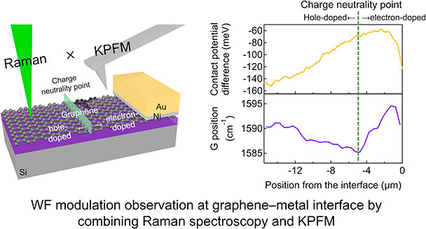
    The semiconductor–metal interface is critical for optimizing the performance of semiconductor devices. For instance, low-resistance Ohmic contacts are essential for high-performance devices like field-effect transistors, while the performance of Schottky junction-based devices, such as diodes and photovoltaics, depends on the formed Schottky barrier height. Generally, the barrier height at the interface does not directly correspond to the work function difference between the semiconductor and metal, showing the difficulty on achieving these devices with ideal performance; this issue persists even for two-dimensional (2D) materials such as graphene and transition metal dichalcogenides. Therefore, developing a reliable method to evaluate the 2D material–three-dimensional metal interface is crucial. In this work, we report an evaluation of the graphene–Ni interface using Kelvin probe force microscopy (KPFM) and Raman spectroscopy. By combining these techniques, we found that the Ni contact exhibited electron doping into graphene, in contrast to the commonly observed hole-doping at graphene–metal contact. We speculate that this discrepancy arises from charge transfer from Ni. Our results emphasize the importance of utilizing KPFM and Raman spectroscopy for a deeper understanding of the graphene–metal interface.

    Download PDF (1783K)
  • Yuta Takaoka, Hiroaki Omori, Hiroyuki Sakaue, Hitoshi Suzuki
    Article type: Regular Paper
    Subject area: Thin Films
    2025Volume 23Issue 2 Pages 113-118
    Published: April 12, 2025
    Released on J-STAGE: May 31, 2025
    Advance online publication: April 12, 2025
    JOURNAL OPEN ACCESS
    Supplementary material

    Self-assembled monolayer membranes formed by amino-alkanethiol molecules have been widely used for modifying Au surfaces because the amino groups are useful for the immobilization of nanomaterials. However, the polarity of the amino group induces irregularity in the membrane; therefore, the structure needed to be analyzed. We analyzed the molecules contained in the membrane formed by amino-alkanethiols on the Au surface using X-ray photoelectron spectroscopy. The molecules that did not combine with the Au surface on the membrane consisted of unbound amino-alkanethiol molecules and the molecules containing sulfur oxide. The ratio depends on the length of the alkyl chain of the amino-alkanethiol molecule. Molecules containing oxidized sulfur were removed by rinsing with a buffer solution (pH 9.1) and ultra-pure water.

    Download PDF (980K)
  • Ryo Imamura, Insung Seo, Hiroyuki Kageshima
    Article type: Regular Paper
    Subject area: Crystal Growth
    2025Volume 23Issue 2 Pages 119-131
    Published: April 12, 2025
    Released on J-STAGE: May 31, 2025
    Advance online publication: April 12, 2025
    JOURNAL OPEN ACCESS
    Supplementary material

    The initial growth mechanisms of intrinsic hexagonal boron nitride (hBN) islands on Cu(111) terraces during chemical vapor deposition (CVD) are investigated using density functional theory calculations. Edge energies are calculated with high accuracy, and critical sizes for previously unexamined island shapes are predicted. The formation energies of small hBN islands are found to be strongly influenced by the curl effect. Through two-dimensional variation of the chemical potential, three of the most stable structures at the critical size—zigzag hexagonal, zigzag boron-edge triangular, and zigzag nitrogen-edge triangular—are identified. Generalization of these shapes enables the drawing of two types of phase diagrams, demonstrating a strong dependence of shape stability on the chemical potential. It is further revealed that maintaining the chemical potential near a specific value is essential for increasing the critical size. These results provide explanations for the experimentally observed hBN island shapes on Cu surfaces during CVD and propose chemical potential conditions for growing hBN films with superior single crystallinity.

    Download PDF (3702K)
  • Wanyu Shi, Daichi Noda, Justian Chandra, Motohiro Tagaya
    Article type: Regular Paper
    Subject area: Nano-Materials
    2025Volume 23Issue 2 Pages 132-137
    Published: May 03, 2025
    Released on J-STAGE: May 31, 2025
    Advance online publication: May 03, 2025
    JOURNAL OPEN ACCESS
    Supplementary material

    We successfully synthesized photoluminescent carbon compounds (CC) hybridized Eu3+ and F ions co-doped hydroxyapatite nanoparticles, and evaluated the photoabsorption and photoluminescence (PL) properties of the nanoparticles with the thermal treatment. Specifically, the intermolecular dehydration occurred between citric acid (Cit) molecules as well as between Cit and L-Cysteine to effectively form the luminescent CC which showed blue-color-emitting by the thermal treatment at 85–140°C. By the thermal treatment at 140°C, the nanoparticles exhibited the wider PL emission color range with the higher internal quantum yield (15.3%) in the combination with Eu3+ ions which showed the red-color-emitting. With the thermal treatment at 140–180°C, the carbonization rate of CC increased and then the luminescent CC was changed into the non-luminescent graphene-like CC, which led the increase in the absorption efficiency, resulting in the purple to pink-color-emitting nanoparticles. From the above, it is possible to control the carbonization rate and the state of CC by the thermal treatment temperature, and realize the nanoparticles with the wider PL emission color range, which is expected to be applied as bioimaging materials.

    Download PDF (1546K)
  • Shigeru Suzuki, Masaki Chiba, Takenori Tanno, Shuichiro Hashi, Kazushi ...
    Article type: Regular Paper
    Subject area: Interdisciplinary
    2025Volume 23Issue 2 Pages 138-142
    Published: May 03, 2025
    Released on J-STAGE: May 31, 2025
    Advance online publication: May 03, 2025
    JOURNAL OPEN ACCESS

    X-ray diffraction (XRD) and scanning electron microscopy (SEM) in combination with electron backscatter diffraction (EBSD) were used to evaluate the residual stresses and microstructure of a functional Fe-Ga single crystal alloy. The single crystal was subjected to electrical discharge machining (EDM) and tensile deformation. A surface layer of polycrystalline grains was formed by EDM, and the residual stress of the single crystal was measured with the surface layer. The residual stresses in the surface layer revealed that the maximum principal stress of the alloy increased along the tensile direction during deformation, the results obtained by SEM-EBSD indicated that band-like microstructures corresponding to the {112}〈111〉 slip system were formed on the fracture surface after deformation. The observed traces of slip surfaces corresponded to deformation twins formed in the alloy. The results evaluated using XRD showed a correlation between the principal residual stresses and the microstructure observed by SEM-EBSD. The large principal stresses were found to be consistent with the direction of the applied tensile stress. Furthermore, the residual stresses were shown to change abruptly from tensile to compressive due to the shrinkage of the alloy at rupture. In addition, the residual stresses were shown to change abruptly from tensile to compressive due to the shrinkage of the alloy at rupture. These results indicate that stress measurements of single crystal alloys can be effectively performed by inducing polycrystals formed on the surface layer by EDM, and provide valuable insight into the stress distribution characteristics of such single crystal alloys due to deformation.

    Download PDF (2366K)
  • H. Tanaka, H. Shinotsuka, H. Yoshikawa, S. Tanuma
    Article type: Regular Paper
    Subject area: Electronic Properties
    2025Volume 23Issue 2 Pages 143-159
    Published: May 03, 2025
    Released on J-STAGE: May 31, 2025
    Advance online publication: May 03, 2025
    JOURNAL OPEN ACCESS

    We measured a series of energy loss spectra (ELS) for GaN, GaP, and GaSb using a 4500 eV primary electron beam over an energy loss range of 1 to 50 eV with angle-resolved reflection electron energy loss spectroscopy. From these ELS data and atomic scattering factors in the range of 50 eV to 30 keV, the energy loss function (ELF) within the range of 1 eV to 30 keV was determined by applying factor analysis and the Kramers-Kronig sum rule. Key results include the identification of various energy loss structures, such as plasmon peaks and band gaps, the derivation of the real and imaginary components of the dielectric function, refractive index, and extinction coefficient. These results were compared with existing experimental and theoretical data, showing consistent trends and providing new insights. The motivation for this study stems from the lack of detailed optical constants for III-V semiconductors in this energy range, which are critical for the analysis of electronic structure and chemical states by X-ray photoelectron and Auger electron spectroscopy. We also calculated and reported two electron transport parameters: inelastic mean free paths (IMFPs) and collision stopping powers (SPs) for GaN, GaP, and GaSb in the energy range of 50 eV to 30 keV. These values were derived from the resulting ELFs using the full Penn algorithm with band gap correction. The IMFP values calculated from the obtained ELF were well-fitted to the energy range of 50 eV to 30 keV using the modified Bethe equation, with a root mean square (RMS) deviation of less than 1%. Moreover, the RMS deviation between the IMFP values calculated in this study and those predicted by the general Jablonski-Tanuma-Powell equation [A. Jablonski et al., Surf. Interface Anal. 55, 609 (2023)] was less than 4% for the three compounds analyzed within the same energy range. Using the mean excitation energy (MEE) values derived from the obtained ELF, the SP was calculated based on the relativistic Bethe SP equation. A comparison showed that the difference between the two values was approximately 5% in the energy range of 2 to 30 keV. Based on these findings, we have proposed a new fitting function derived by extending the relativistic Bethe SP equation to describe the energy dependence of SP over a wide range from 50 eV to 30 keV. By applying this fitting function, the SP values for the three compounds examined in this study could be reproduced with an RMS deviation of less than 3% across the energy range of 50 eV to 30 keV using four parameters.

    Download PDF (2044K)
  • Valeri Lozovski, Nataliia Rybalchenko, Iryna Petrik, Kostiantyn Kryvok ...
    Article type: Regular Paper
    Subject area: Interdisciplinary
    2025Volume 23Issue 2 Pages 160-167
    Published: May 15, 2025
    Released on J-STAGE: May 31, 2025
    Advance online publication: May 15, 2025
    JOURNAL OPEN ACCESS

    The present paper deals with experimental and theoretical studies of the antibacterial action of the nanostructured gold surface against Staphylococcus aureus ATCC 6538 (S. aureus). The primary purpose here is to answer whether the enhancement of the antibacterial effect of a nanostructured gold surface under the conditions of plasmon resonance takes place. For the reliability of our investigations, we use four identical samples of bacteria suspensions. They are the control sample which is reserved at room temperature in the darkness, the pumped sample, and the samples for the experiments when the suspension contacts the gold surface under and without surface plasmon (SP) resonance conditions. We use two experimental approaches. The bacterial suspension circulated along the metal surface is studied. Also, the case of bacteria slowly settling onto the gold surface under gravity is considered. Experiments in the case of suspension circulation discover the near-double enhancement of the antibacterial action of the gold surface against S. aureus under SP resonance conditions. The enhancement results from the increased interaction between the bacteria and the gold surface under these conditions. The adsorption potential is increased up to ten times when the SP is excited along the surface. As a result, the local-field enhancement effect is increased, which leads to an increase in the area of strong gradients of a local field and, thus, an increase in the act of ponderomotive forces. These forces are the reason for bacterial membrane damage.

    Download PDF (1670K)
  • Ryo Ozaki, Masahiro Ohara, Manato Tateno, Hisao Ishii
    Article type: Regular Paper
    Subject area: Instrumentations and Techniques
    2025Volume 23Issue 2 Pages 168-173
    Published: May 17, 2025
    Released on J-STAGE: May 31, 2025
    Advance online publication: May 17, 2025
    JOURNAL OPEN ACCESS

    Understanding the electronic structures of materials under environmental conditions, such as in the atmosphere, has gained significant attention for applications in catalytic chemistry and improving air stability in organic electronics. Recently, near-ambient pressure photoelectron spectroscopy (NAP-PES) has been developed, enabling measurements even at atmospheric pressure using differential pumping and powerful light sources. Although NAP-PES is a well-established and powerful method, it faces practical challenges. First, the environment around the sample surface is dynamic, influenced by gas flow due to differential pumping. Second, the apparatus is expensive, and machine time is limited, particularly in synchrotron radiation experiments. In contrast, photoelectron yield spectroscopy (PYS) for measuring ionization energy and work function, which is simpler and more affordable than NAP-PES, has been used in both vacuum and atmospheric environments in semiconductor device research. However, PYS cannot determine the density of states (DOS). This study focuses on ultraviolet photoelectron spectroscopy (UPS) using a classic retarding field analyzer (RFA) in current-detection mode. By measuring UPS spectra of highly oriented pyrolytic graphite under varying vacuum pressures, ranging from ultrahigh vacuum to over 100 Pa, we found that photoelectron kinetic energy distribution could be obtained even at pressures where the electron flight length in the RFA is seven times the photoelectron’s mean free path. The feasibility of UPS, PYS, and constant-final-state yield spectroscopy was further demonstrated by measuring the spectra of a C60 film under different vacuum conditions. Changes in the DOS of the C60 film due to oxygen and/or water molecules under medium vacuum conditions were clearly observed. Thus, photoelectron spectroscopy using an RFA in low to medium vacuum conditions is feasible. The apparatus is inexpensive and robust, offering potential for future use by researchers in device development to survey various materials for electronics under practical conditions.

    Download PDF (2890K)
  • Hikaru Iwatani, Fumihiko Maeda
    Article type: Regular Paper
    Subject area: Nano-Materials
    2025Volume 23Issue 2 Pages 174-181
    Published: May 17, 2025
    Released on J-STAGE: May 31, 2025
    Advance online publication: May 17, 2025
    JOURNAL OPEN ACCESS
    Supplementary material

    We investigated the growth of graphene on silver surfaces by chemical vapor deposition (CVD) with ethanol as the gas material under various growth conditions. The investigation was based on Raman spectroscopy analysis. We determined that over 900°C is required to decompose the ethanol. Additionally, we proposed a graphene growth mechanism on the silver surfaces. Herein, the formation of the graphene nuclei and silver evaporation are competing processes, which limits the crystallinity of the graphene. Furthermore, we demonstrated that the addition of hydrogen during the CVD growth and the modifications of the conditions of the sample cooling process after the growth are valid for expanding the growth conditions and improving the crystallinity of graphene. The modifications included a low cooling rate of the substrates, maintenance of the environmental pressure equal to that of the growth, and a continuous supply of ethanol after the growth. The results indicate that the suppression of silver atom evaporation is the key to obtaining high-crystallinity graphene.

    Download PDF (2093K)
  • Reiji Takeda, Fumihiko Maeda
    Article type: Regular Paper
    Subject area: Nano-Materials
    2025Volume 23Issue 2 Pages 182-187
    Published: May 17, 2025
    Released on J-STAGE: May 31, 2025
    Advance online publication: May 17, 2025
    JOURNAL OPEN ACCESS

    We investigated the growth of graphene on a Ge(110) substrate using photoresist as the source of the solid material. First, we elucidated that a substrate temperature of 900°C was suitable for graphene growth. Subsequently, graphene was grown on the Ge surfaces under various conditions: we found that the optimal heating time was 3 min, and that the addition of hydrogen to the ambient gas flow improved the crystallinity of the graphene. Furthermore, we found that methoxybutyl acetate was a more suitable solvent for diluting the photoresist than acetone, as the resulting resist thin film exhibited less roughness before heating, which improved graphene crystallinity. Finally, from examining the effect of the flow rate of the mixture gas of Ar and H2, a drastic change in the graphene surface morphology was observed, which resulted from the mass transport of an extremely large amount of the substrate material. This phenomenon might have limited the crystallinity of the graphene and, therefore, should be suppressed in order to grow high-quality graphene using this method.

    Download PDF (1787K)
  • Kentaro Miyamoto, Koji Shimizu, Anh Khoa Augustin Lu, Satoshi Watanabe
    Article type: Regular Paper
    Subject area: Interdisciplinary
    2025Volume 23Issue 2 Pages 188-192
    Published: May 17, 2025
    Released on J-STAGE: May 31, 2025
    Advance online publication: May 17, 2025
    JOURNAL OPEN ACCESS
    Supplementary material

    High entropy alloys (HEAs) are expected to show excellent performance in various fields, such as catalysts and high-temperature structural materials, but the huge number of configurations makes it difficult to find the optimal compositions for HEAs. In this study, machine learning potentials were developed to accurately predict the total and H/CO adsorption energies of multi-element slab models and cluster models of various sizes and shapes, based on density functional theory calculations.

    Download PDF (1967K)
  • Muneaki Yamamoto, Shinya Mizoguchi, Tetsuo Tanabe, Tomoko Yoshida
    Article type: Regular Paper
    Subject area: Catalysis
    2025Volume 23Issue 2 Pages 193-198
    Published: May 17, 2025
    Released on J-STAGE: May 31, 2025
    Advance online publication: May 17, 2025
    JOURNAL OPEN ACCESS

    Cu-In catalysts with different mole ratios were prepared and conducted to the electrochemical CO2 reduction on gas diffusion electrodes. All the Cu-In catalysts showed higher activity for CO production than In and Cu single catalysts. The activity changed remarkably with Cu-In mole ratio, and the catalyst with Cu-In mole ratio of 20:1 showed good performance in electrocatalytic CO2 reduction giving the CO production rate of 32 µmol h−1 with a Faraday efficiency of 81.0% and a current density of 2.3 mA cm−2 at maximum under the cell voltage of 2.2 V. X-ray diffraction, X-ray photoelectron spectroscopy, and X-ray absorption fine structure analyses revealed the dynamic change in the chemical state and structure/morphology of Cu-In catalysts before and after the reaction, i.e., CuO and In(OH)3 or In2O3 were mainly formed before the reaction whereas CuO changed to CuCO3 and Cu(OH)2 after the reaction. In addition, Scanning electron microscope-energy dispersive X-ray spectroscopy observations clearly indicated the difference in morphology of high and low active Cu-In catalysts after the reaction; In species was segregated on the Cu surface in the former catalyst while it completely covered the surface of the latter catalyst. These results suggested that the interface of In(OH)3 or In2O3 and Cu species should play a key role in the electrocatalytic CO2 reduction.

    Download PDF (4326K)
Conference-ISSS-10-
  • Masamichi Yamada, Yudai Sato, Masahiro Haze, Yukio Hasegawa
    Article type: Proceeding Paper
    Subject area: Structure
    2025Volume 23Issue 2 Pages 199-206
    Published: April 12, 2025
    Released on J-STAGE: May 31, 2025
    Advance online publication: April 12, 2025
    JOURNAL OPEN ACCESS

    Striped-incommensurate (SIC) phase is formed on Si(111) around lead (Pb) coverage of 1.30. The structure of the SIC phase is difficult to analyze, since it is incommensurate. Even an approximate model requires a large unit cell. In this paper, we propose a simple model based on a ball model, and show that the driving force which leads to SIC phase is compressive stress inherent to a hypothetical perfect (√3×√3)R30° Pb arrangement on Si(111). The stress is relieved by uniaxial [-110] expansion of the Pb layer and subsequent slight twin-like deformation. The modification enables Pb atoms to occupy stable H3 sites or T4 sites as many as possible, and makes stable the resultant arrangement. We show that these models well account for various features observed with scanning tunnelling microscopy. We also apply our model to devil’s staircase reported around similar Pb coverages, and show that higher-coverage phases in devil’s staircase family should be understood with our model.

    Download PDF (5194K)
  • Hinako Telengut, Boxuan Li, Kenya Haga, Tadashi Abukawa
    Article type: Proceeding Paper
    Subject area: Structure
    2025Volume 23Issue 2 Pages 207-212
    Published: May 03, 2025
    Released on J-STAGE: May 31, 2025
    Advance online publication: May 03, 2025
    JOURNAL OPEN ACCESS

    It is known that when Si(551) substrates are heated in an ultrahigh vacuum, Si(551) substrate is faceted to form a ridge-and-valley nanotexture. In this study, the facet plane was determined to be (17 15 3) by means of the precise analysis of the reflection high energy electron diffraction (RHEED) and the scanning tunneling microscopy (STM). RHEED results concluded that 3 × 1 super structure was formed on the Si(17 15 3) as a stable structure. STM images showed that parallel grooves were running parallel to [015] direction. The spacing between the grooves was random after flashing at 1250°C, but converged into the 3 × 1 periodicity after annealing at 700°C. The (17 15 3) surface must be crystallographically homo chiral. In the STM image of the 3 × 1 structure, three protrusions were arranged between the grooves. The present results inferred that the ridge-and valley structure of Si(551) consists of the chiral (17 15 3)3 × 1 and its enantiomorph (15 17 3)3 × 1. Such alternative chiral nano-texture is a promising substrate for the formation of novel chiral materials.

    Download PDF (1922K)
feedback
Top