Review Papers
Assembly of Nanoparticles: Towards Multiscale Three-Dimensional Architecturing
2013 Volume 30 Pages 31-46
Details
2013 Volume 30 Pages 31-46
Fundamental building block in nanotechnology is the nanoparticle and currently many excellent techniques are available to control its size, morphology and crystalline phase at mass quantity. However, the practical realization of novel nanodevices employing nanoparticles requires the construction of multiscale three-dimensional buildings consisting of the basic building block, nanoparticles, particularly as an ordered array, which remains challenging. In this review, we address various methodology developed for the assembly of nanoparticles by classifying them depending on manipulating force. Methods utilizing electric, capillary, and magnetic forces are discussed. Ion assisted aerosol lithography(IAAL) that utilizes ion induced focusing concept will be described in more detail since it provides an opportunity for multiscale multidimensional assembly of nanoparticles in a parallel fashion at atmosphere.
Significant advances have been made in synthesizing nanomaterials including organic molecules, nanoparticles and biological molecules. Especially, for nanoparticles, there has been great progress in developing methodologies for controlling their size, shape and crystalline phase in the past decade1–16). Along with these advances, deposition of nanoparticles or molecules on desired position of a substrate with nanoscale resolution has received great attention in recent years, due to its promising potential to realize nanodevices for various applications in the fields of electronics, optics, chemistry, and biomedics17–28). The realization of emerging convergence technology requires us to have control capability on multiscale phenomena including nano, micro, and macro scales. Bridging among different scales is a prerequisite for manufacturing practically various novel nanodevices exhibiting unprecedented performance, which include nano-bio sensors, nano-electric/optical/magnetic devices and nano-energy devices. Such ultimate integration among different scales in three dimensions can be called as multiscale three-dimensional architecturing which is challenging and demanding, but worthwhile to explore since it can become an important platform for convergence technology. A variety of techniques have been introduced to carry nanomaterials onto a surface in a serial or a parallel manner, consequently, to form patterns or arrays of the materials. We first review various methods of patterning nanomaterials (generally nanoparticles) according to the governing force employed to manipulate nanoparticles. In this review, we limit our discussion to the forces of electrostatic, capillary and magnetic forces, which are the three most frequently used forces in manipulating nanoparticles. Recently, methods for improving pattern resolution by producing a nanoparticle pattern with width smaller than the original pattern utilizing the focusing capability caused by electrostatic interactions have been reported such as electrodynamic focusing of charged aerosols, electrostatic funneling using surface treatment and p-n junction based electrostatic method. Among the electrodynamic focusing methods of charged aerosols, Ion Assisted Aerosol Lithography (IAAL) is a parallel atmospheric process for assembling nanoparticles in multiscale three dimensions with nanometer resolution thanks to the ion induced focusing capability. We will focus on this IAAL technique in the second part of this review. Finally, device applications based on nanoparticle assembly demonstrated by IAAL will be discussed.
The use of electric fields is the most common approach to transport and assemble a large number of small particles in a parallel fashion because electrostatic interaction is long-range and non-material-specific29). Micro- or nanosized particles can be trapped within the charged areas formed on the substrate surface leading to produce a particle pattern. Due to its effectiveness, there has been great interest in developing techniques to manipulate nanoparticles with high precision by means of electrostatic force on a large area. In this section, we will address on charge-writing method, nanoxerography, electric field induced aerosol method, biased p-n junction method, and electrostatic funneling method.
Charge-writing methodLocalized charge patterns have been widely utilized to make patterns of nanoparticles because, just by exposing the substrate to a suspension of nanoparticles, the particles experience long-range Coulomb interactions and are selectively deposited on the charged area of the substrate30–32). A stainless-steel needle was used to create lines of negative charges by contact charging on the surface of a oxidized silicon substrate33). Charges maintained in the insulator for hours after the metal was removed34). Then, charged aerosol particles were directly positioned along the patterns of surface charges on the insulating substrate. A conductive tip of an atomic force microscope (AFM) could be also used to deposit localized charge patterns on an electret followed by immersion of the substrate into a suspension of nanoparticles to form a pattern of the nanoparticles35). Similar processes were conducted but the use of a focused ion beam (FIB), as shown in Fig. 1(a), in forming patterns of surface charges and two-dimensional arrays were obtained as a result36, 37). Although this method can provide fine structures of nanoparticles, the process to create surface charges with a conductive needle is a serial and time-consuming process and this method cannot be applied to conducting substrates.
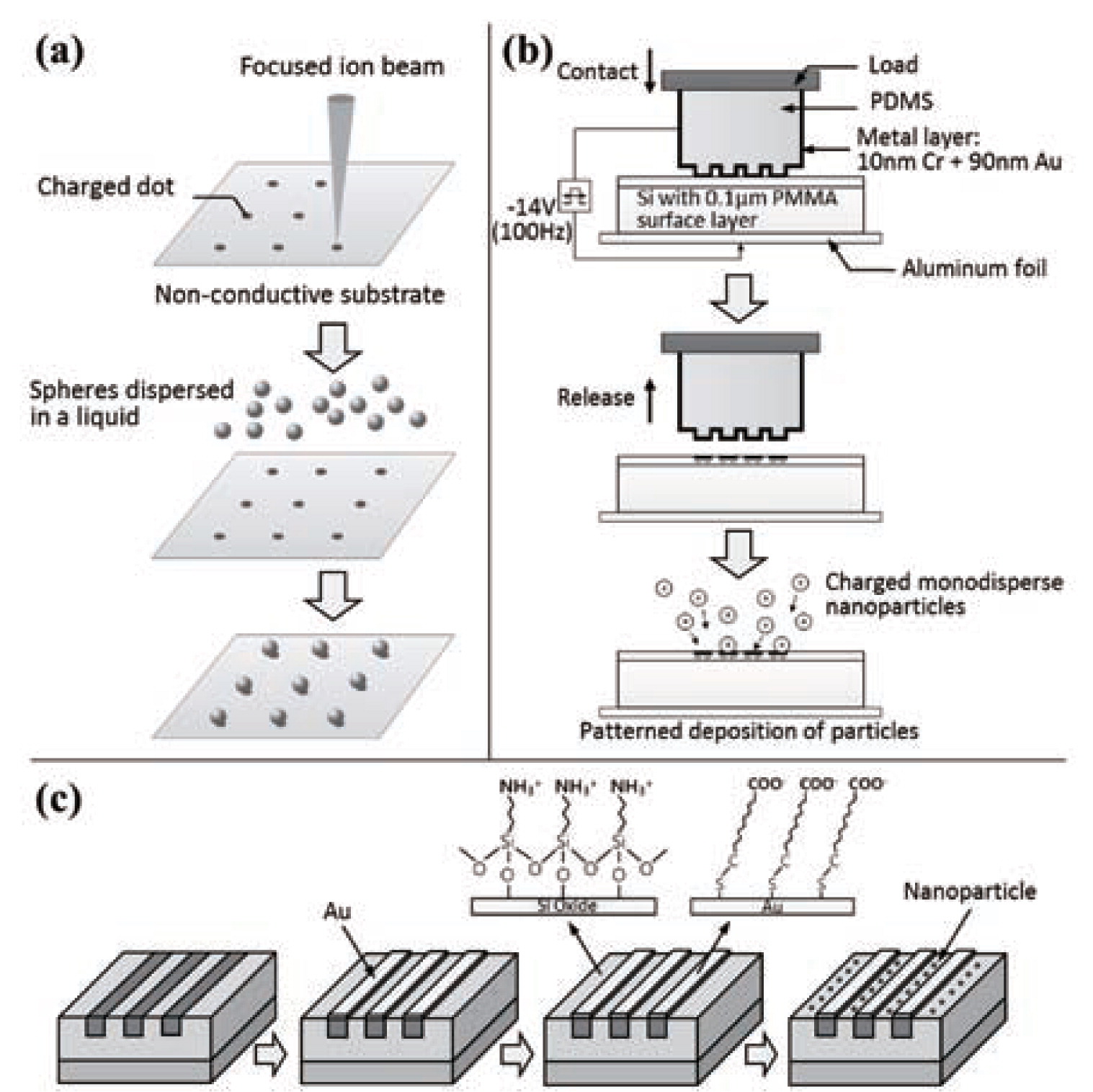
(a) A schematic illustration of the steps to fabricate two-dimensional particle arrays using a charged pattern. A charged pattern is formed on an insulating substrate by scanning a charged beam in vacuum. Reprinted with permission from ref 36. Copyright 2002 Wiley-VCH. (b) A schematic illustration of the process of parallel charge patterning and nanoparticle deposition. A pulse voltage of −14V (100Hz) was applied between the PDMS stamp and the substrate for about 10s to generate charge patterns onto the substrate. Reprinted from ref 38, Copyright 2004, with permission from Elsevier. (c) A schematic illustration of the experimental process to place nanoparticles onto silicon oxide lines using electrostatic funneling scheme. Lines of nanoparticles appear as a result. Reprinted with permission from ref 48. Copyright 2007 American Chemical Society.
Nanoxerography is a parallel method to fabricate nanoparticle arrays by utilizing a conductive flexible stamp with patterns that can transfer charge patterns on non-conducting surface in a single step38–40). Fig. 1(b) shows a process of transferring charges on a poly(methylmethancrylate) (PMMA) thin film in parallel and depositing nanoparticles on the area of charge patterns. A poly(dimethylsiloxane) (PDMS), patterned in bas-relief, was made electrically conducting by forming 80-nm thick gold film with thermal evaporation on it. For the generation of charge patterns, a metal-coated PDMS stamp was placed on top of the 80-nm thick PMMA film supported on an n-doped silicon wafer and a voltage of 10 to 20-V was applied between the gold on the PDMS and the back side of the silicon. With this method, Jacobs and Whitesides29) showed that transfer of charge patterns ranging from 120-nm to 100-μm in size onto the PMMA was possible in less than 20s, and produced particle patterns by dipping the substrate into dry powders. During the process of coating the PDMS stamp with metal through thermal evaporation, buckling of the metal coating can appear due to thermal expansion and contraction of the PDMS stamp41). To prevent the buckling, a sputtering method38) has been suggested. In addition, uniform contact between a stamp and a substrate in large area and fabrication of reliable stamps with nanoscale resolution are issues. It is also noted that nanoxerography cannot be utilized for conducting surface.
Electric field induced aerosol deposition methodUnder a given electric field, Prost et al.42) and Otten et al.43) deposited singly charged lead sulfide (PbS) nanoparticles generated by aerosol techniques onto a GaAs substrate which is patterned with different resist structures having a minimum feature size of 600-nm. A lift-off process after particle deposition removed the resist while the patterns of deposited nanoparticles remained. It was observed that the size of deposited structures was smaller than the open area of the photoresist. This result was attributed that the resist was selectively charged by the deposition of charged particles and further deposition of the incoming particles on the resist are repelled by the predeposited particles with the same charge polarity. Similar approach utilizing the effect of electrostatic focusing caused by charged particle deposition was also reported by Jun et al.44). It is noted that charged particles should deposit everywhere randomly including on the photoresist surface and the exposed GaAs surface until sufficient amount of charged particles deposit on the photoresist surface to begin to show focusing phenomenon. Similar focusing phenomenon due to the deposition of charged particles was also observed when a Teflon mask was used during electrospraying45). On the other hand, the method utilizing ion induced focusing that our group developed enables electrodynamic focusing of charged aerosols46) from the start without generating noise particle deposition. We call this method as “Ion Assisted Aerosol Lithography (IAAL)” since the ion injection is a crucial step to enable focused deposition of charged aerosols producing multiscale and three-dimensional architectures consisting of nanoparticles as basic building blocks for structures with nanoscale resolution. We will discuss this in full detail later.
Biased p-n junction methodTsai et al.47) developed a method of positioning metal nanoparticles delivered from a gas phase onto surfaces using electrostatic force generated by biased p-n junction patterned substrates. They prepared a p-n junction patterned substrate by fabricating 1-μm wide p-type lines on an n-type GaAs substrate using photolithography and charged nickel nanoparticles by aerosol technique. The negatively charged particles were repelled from the p-type regions and attracted to the n-type regions, particularly at the interface of p-n junctions, where the local field was the highest. If the polarity of the particle was changed to positive, the particles were attracted to the depletion zone of the p-type regions and were repelled from the n-type regions. As the reverse bias on the substrate increased, almost all the negatively charged nickel nanoparticles were deposited on the n-type regions. Although many noise particles existed on the resulting substrates, it is advantageous that this assembly method can be applied to commonly used substrate architectures and provide nanoparticle patterns quite easily on a large area.
Electrostatic funneling methodElectrostatic funneling was proposed by Ma et al48) as a way to place nanoparticles onto predefined locations on a substrate in large area. As described in the Fig. 1(c), the substrate was prepared to have alternating lines functionalized with positively and negatively charged molecules. When the substrate was dipped into a suspension of negatively charged gold nanoparticles, the particles were electrostatically guided onto the centers of the positively charged lines and deposited along the lines. Here, it was experimentally shown that the nanoparticles were funneled away from the boundary toward the center of the positively charged area when the electrostatic interaction energy gradient was strong while they were not when the gradient was weak. This method is simple and compatible with CMOS fabrication and packaging technology, but some treatments are needed to change the electrostatic interaction energy gradient as well as surface treatment.
1.2 Capillary force directed assemblyThe phenomenon of capillarity has been given attention as another possible means to assemble particles49–54). It can be commonly observed that floating particles become clustered when liquid evaporates. This is because, when two such particles are close to each other, the deformed interface around them is not symmetric as the interface height between them is lowered due to the interfacial tension, and the particles come to experience attractive capillary force between them51, 53). Based on this capillary phenomenon, deposition from a suspension of colloids has provided two- and three-dimensional arrays of crystal-like structures of particles55–58), the mechanism of which usually involves aggregation initiated by capillary force, growth driven by a laminar flow, and evaporation of the solvent59). In this section, we will discuss some representative and interesting researches which have been carried out to manipulate particles by utilizing capillary force according to the following subjects: micromolding in capillaries, template-assisted assembly, and dip-pen nanolithography.
Micromolding in capillariesKim et al.60) fabricated crystalline two- or three-dimensional arrays of microspheres using micromolding in capillaries61). Fig. 2(a) outlines the experimental process of micromolding in capillaries. An elastomeric mold with a relief pattern was made from PDMS and both ends of the channels in the mold were cut to allow the fluid to enter and escape. A network of channels was formed by placing the mold on a support. When a drop of a latex solution containing polystyrene microspheres was placed at one end, the fluid filled the channels by capillary action. As the liquid evaporates, the microspheres crystalized on the support within the confinement of the channels and, finally, lines of crystallized microspheres were obtained after the removal of the PDMS. They also fabricated more complex patterns of crystallized microspheres using this technique.
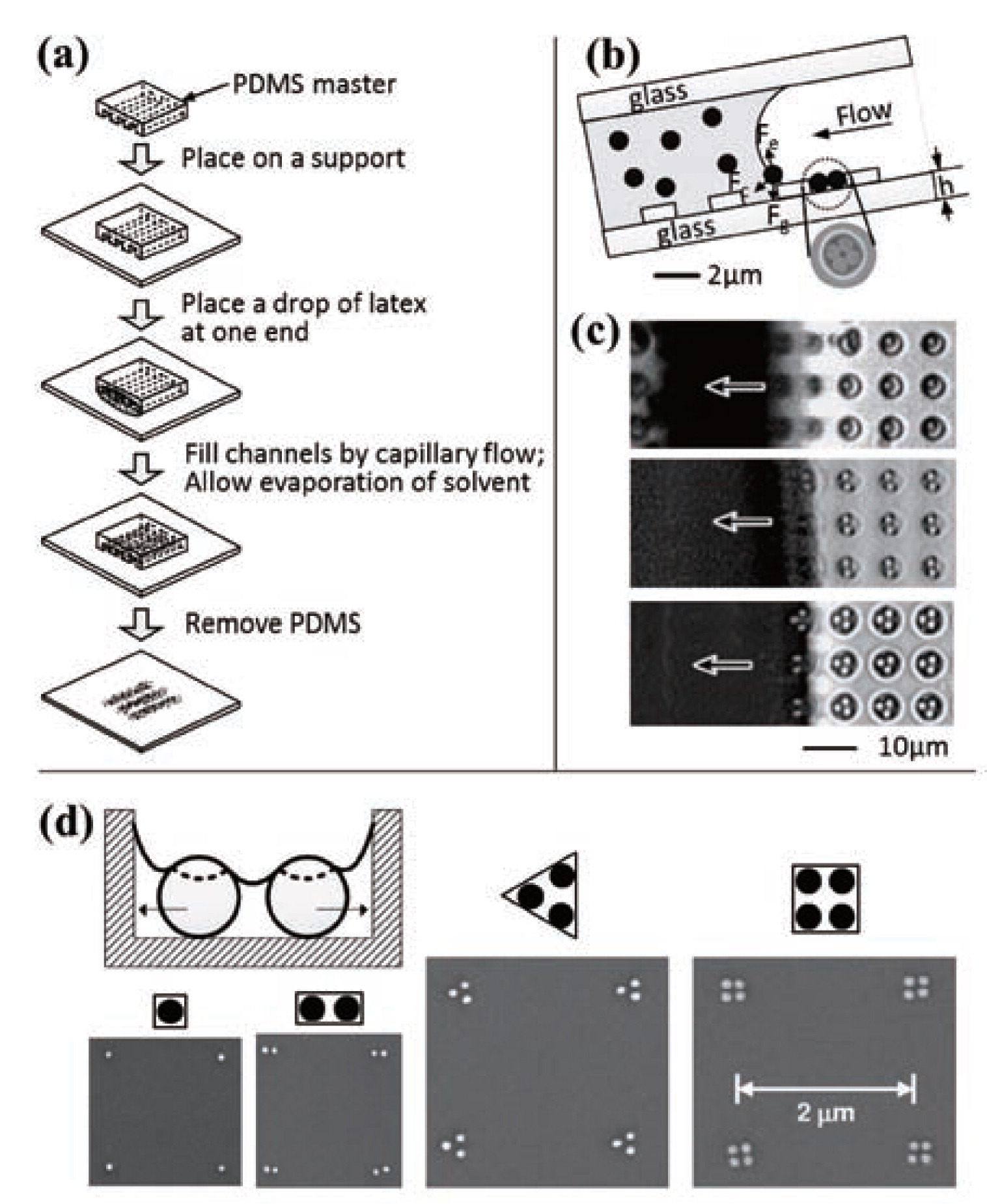
(a) A schematic illustration for the process of micromolding in capillaries. Reprinted with permission from ref 60. Copyright 1996 VCH. (b) A schematic illustration of the process to generate aggregates of spherical colloids under the physical confinement of templates. A colloidal particle next to the rear edge of the liquid slug experiences three possible forces there: the capillary force (Fc), the gravitational force (Fg), and the electrostatic force (Fe). (c) Optical micrographs showing the assembly of polystyrene beads with different sizes into cylindrical holes with different sizes. (b) and (c) are reprinted with permission from ref 65. Copyright 2003 Willey-VCH. (d) A schematic illustration of the particle separation due to the probable free surface of the liquid in a pattern and the experimental results of the assembly of particles which are preferably positioned at the corner of each pattern. Reprinted with permission from ref 63. Copyright 2006 American Institute of Physics.
Similar but template-assisted fabrication methods using colloids have been demonstrated62–67). Xia et al. fabricated colloidal aggregates by dewetting aqueous dispersions of monodispersed spherical colloids across surfaces patterned with two-dimensional arrays of relief structures as shown in Fig. 2(b) and (c). As the liquid was slowly de-wetted from the confined space, the spherical colloids were pushed into the templates which was influenced by the capillary force originated from the liquid meniscus, and consequently formed a densely packed structure. With this approach, they demonstrated not only homo-aggregates of silica beads, including circular rings, polygonal and polyhedral clusters, linear zigzag and spiral chains, but also hetero-aggregates containing spherical colloids of different sizes, compositions, densities, functions, or a combination of these features. However, the size of colloids they could successfully make use of was limited down to 50-nm due to the limitation of their ability to fabricate templates on such a small scale. Cui et al.62) successfully assembled macromolecule-sized gold nanoparticles with diameters of less than 10-nm. Flat substrates patterned with hole and trench template were inserted vertically into a solution containing nanoparticles of interest. During the evaporation of the solvent, three-phase contact line moved slowly across the substrate, and the resulting capillary force pushed the particles into the denser parts of the solution when the evaporation zone passed over them. They also demonstrated to assemble anisotropic nanostructures such as tetrahedrally-shaped CdTe nano-tetrapods with 4-nm side and ∼100-nm long arms. Gordon and Peyrade63) presented arrays of one to four closely spaced nanoparticles, as shown in Fig. 2(d), by controlling template shape and wettability. These arrays could be utilized as an etching mask for pattern transfer via reactive ion etching. Kraus et al.64) developed a technique of printing nanoparticles with single-particle resolution. Here, sub-100-nm nanoparticles were individually placed by capillary force at the positions that were defined by the geometry of a template, and subsequently transferred to a second substrate having a higher level of particle adhesion than the printing plate.
Dip-pen nanolithographyDip-pen nanolithography (DPN), a method for directly depositing molecules via capillary transport of molecules by an atomic force microscope (AFM) tip to the solid substrate, was originally designed to work on gold surfaces68). However, metal surfaces are not desirable for many of applications in electronics, photonics and sensing69–74). Therefore, there have been studies to deposit metal nanoparticles as dots or lines of clusters on various substrates using DPN or other AFM-based methods74–80). Ben Ali et al.77) directly positioned gold nanoclusters on a silica surface by first depositing a small volume of solution of the clusters using DPN, then letting the solvent evaporate. Here, the size of deposited islands was strongly dependent on the contact force between the tip and the surface. In contrast, Tomas et al.79) presented that pattern dimensions were independent on the applied contact force. The DPN experiments were carried out on mica substrates employing hydrosols containing chemically prepared lead nanocrystals and gold nanocrystals, and, notably, no lateral diffusion of the ink was observed. Garno et al.78) also suggested a method to limit lateral diffusion of delivered patterns from a tip to a substrate by utilizing a covalent linkage between the gold nanoparticles and the substrate surface modified with a self-assembled monolayer (SAM). Further studies have been carried out to overcome low throughput of the DPN technique which is presumably caused by depletion of the ink. A microfluidic nanofountain probe has been developed for continuous feeding of the ink. With this approach, Wu et al.80) fabricated arrays of 200-nm-diameter dots with gold nanoparticles and Taha et al.74) did arrays of 100-nm-wide lines. However, unlike other small molecule-based inks, it is still relatively difficult to make AFM tips coated uniformly with metal nanoparticles because of their large size81), and, consequently, it is difficult to obtain a uniform nanoparticle array with a controlled number of particles using DPN82). It is also noted that DPN is inherently a serial method.
1.3 Magnetic force directed assemblyAlthough there has not been much research on the manipulation of particles utilizing magnetic force in comparison to the cases of utilizing electrostatic and capillary force, there have been some efforts on assembling particles employing magnetic force83–87). Wolf and Birringer85) demonstrated a two-dimensional carpetlike array of magnetic rods by depositing aerosol-grown magnetic iron nanoparticles onto a substrate in the presence of homogeneous magnetic field. The formation of regular patterns in the two-dimensional array of elastically deformable magnetic rods was attributed to the magnetic dipolar interaction between the bundles. Ennen et al.83) presented a method to manipulate the assembly of magnetic nanoparticles by applying stray fields of magnetically patterned ferromagnetic layers which were pinned by the exchange bias interaction (EB)84) to a neighboring antiferromagnetic layer. The magnetic patterning was generated by bombarding 10-keV He ions onto the areas to be patterned by nanoparticles in the presence of a magnetic field. On the other hand, Yellen et al.87) introduced a method for assembling non-magnetic colloidal particles with sizes ranging from several micrometers down to less than 100-nm into highly regular patterns by exploiting magnetic force. Here, magnetic force on nonmagnetic particles was transmitted through a fluid dispersion of magnetic nanoparticles, such as ferrofluid. The magnetization patterns as a template for producing reprogrammable magnetic field map were created by ferromagnetic thin film with discrete patches fabricated by lithographical patterning. With this technique, assembly of micrometer- and submicrometer-sized beads onto the magnetic traps of various shapes could be obtained.
In the IAAL process, both charged aerosols and ions having the same polarity are injected together into an electrostatic precipitator (ESP) chamber in which a conducting pre-patterned substrate with a dielectric material, generally a photoresist, is located46). Although charged aerosols and ions are fed into the ESP chamber together, ions, whose mobility is two orders of magnitude greater than charged aerosols, can reach the substrate first. The ions landing on the exposed surface of the conducting substrate are immediately neutralized while those on the photoresist surface become accumulated. These accumulated ions on the photoresist surface distort the initially flat equipotential planes into convex equipotential planes, which act as nanoscopic electrostatic lenses around the photoresist patterns as shown in Fig. 3(a). Consequently, the charged aerosols following behind the ions are convergently guided into the center of the openings in the photoresist since charged particles should move in the direction perpendicular to the convex shaped equipotential planes. In addition, the ions accumulated on the photoresist surface form repelling fields, which serves to avoid generating deposition of noise particles on the photoresist surface and improve particle collection efficiency. As the deposition of nanoparticles proceeds, the focused deposits can develop to three-dimensional structures of multiple nanoparticles as shown in Fig. 3(b)–(c). More details of the three-dimensional assembly will be discussed later. Following the removal of the photoresist, a micro- or nanoarray composed of nanoparticles is finally obtained. Fig. 4 shows some examples of focused patterns fabricated using IAAL46, 88). Fig. 4(a) and (b) shows the arrays of deposited patterns consisting of multiple 10-nm silver nanoparticles on the silicon substrate with the prepatterned photoresist having 230-nm wide dots with 230-nm thickness on it. Here, the invisible electrostatic lenses formed by the accumulated ions on the photoresist surface lead the incoming silver nanoparticles onto the center regions of the exposed Si surface while hindering them from depositing on the photoresist surface. It is clearly shown that silver nanoparticles are assembled in 75-nm dots in Fig. 4(a), which means that the focusing effect of IAAL reduced the width of the particle patterns to about one-third of that of the original 230-nm photoresist prepatterns. An appropriate photoresist stripping process utilizing acetone and deionized water can remove the photoresist layer, which finally generates the focused patterns of silver nanoparticles as shown in Fig. 4(b). It is noted that IAAL enables to fabricate a micro- or nanoarray of nanoparticle assembly whose feature size is much smaller than that of the original photoresist patterns by the ion-induced focusing effect in IAAL. It is also noted that any nanoparticles can be used to the IAAL mediated deposition once they are prepared in the form of charged aerosols. Kim et al.46) electrosprayed a suspension of monodisperse 20-nm gold nanoparticles which were commercially available to lead them to the IAAL system in the form of charged aerosols and fabricated focused assembly of the gold nanoparticles. Focused assembly of proteins were also demonstrated by Woo et al.88) by delivering electrosprayed protein nanoparticles to the IAAL system. Fig. 4(c) shows that human IgG was convergently deposited onto the center regions within 2-μm line patterns of SiO2, which indicates the possibility of the selective immobilization of proteins onto the desired locus88, 89). The fluorescence image of Alexa 488 through confocal laser scanning microscope (CLSM) in Fig. 4(d) confirms the reaction of the Alexa Fluor 488-tagged anti-human IgG and the deposited human IgG, which verifies the protein activity after the deposition. Protein nanoarrays up to 50 nm scales were also produced via the same method in a parallel fashion.

A schematic illustration of the process to develop nanoparticle structures to three-dimensional structures using IAAL. The blue solid lines indicate the electric field and the red solid lines indicate the equipotential lines.

(a) A SEM image of 75-nm dot arrays of 10-nm Ag particles formed within 230-nm PR square patterns. (b) A SEM image of 70-nm dot arrays of 10-nm Ag particles after the removal of the photoresist layer. (a) and (b) are reprinted with permission from ref 46. Copyright 2006 Nature Publishing Group. (c) A SEM image of patterned human IgG. (d) A fluorescence image of Alexa 488-tagged monoclonal goat anti-human IgG (absorption 495-nm, emission 519-nm) with CLSM. (c) and (d) are reprinted with permission from ref 89. Copyright 2010 Willey-VCH.
The deposition configuration of the charged aerosols can be predicted by computing Lagrangian particle trajectories39). In IAAL, the motion of the nanosized charged aerosols in a gas flow under external electric field can be described by the following Langevin equation considering the fluid drag force(FD), Brownian diffusion force(FB), Coulomb force(FC) and van der Waals force(FvdW):
As mentioned earlier, IAAL provides focused deposition of nanoparticles of interest with smaller size than the prepatterned openings on a substrate. The representative process parameters include surface charge density, applied voltage, the aspect ratio of photoresist patterns and the charges of particles. Details of each process parameters will be discussed below.
The magnitude of surface charge density can be easily controlled by changing the ion flow rates. Fig. 5 shows the comparison of the configurations of particle depositions investigated with both experimental and computational methods according to different surface charge densities90). The particle depositions were carried out within 230×230-nm2 square photoresist patterns (thickness ∼135-nm) using IAAL. Fig. 5[(a),(d)], [(b),(e)], and [(c),(f)] are the cases of surface charge density of 3.6×10⁻⁵ C/m2, 2.66×10⁻⁴ C/m2, and 7.57×10⁻⁴ C/m2, respectively. The cases of no ion injection, Fig. 5[(a),(d)], of which surface charge density is arisen from the charged particles deposited on the photoresist, show that 10-nm silver particles are randomly deposited all over the surfaces including the photoresist surface and the exposed silicon surface. A little focusing of the particles near the exposed silicon surface even without ion injections is attributed to the charges of the deposited particles on the photoresist surface, which was previously observed42, 45). It is clearly shown that the deposited pattern under higher surface charge density forms a more focused feature. It also can be seen that the flat equipotential lines, indicated by the pink solid lines in the particle trajectory simulation, for the case of no ion injections are strongly modified into convex as the surface charge density increases, and, accordingly, a large number of particles are effectively guided into the center region of the opened Si surface. When the surface charge density increases to 7.57×10⁻⁴ C/m2, about a 35-nm dot pattern consisting of multiple 10-nm Ag particles was formed within the 230-nm wide photoresist pattern, which indicates that the ion-induced focusing effect reduced the feature size of the particle assembly to about one-seventh of the original photoresist pattern. The higher surface charge density enables not only the greater focusing effect but also the stronger screening effect. As shown in the computational results in Fig. 5, particles are remarkably suppressed to land on the photoresist surface as the surface charge density increases, which reflects that Brownian motion of the particles approaching the substrate is suppressed near the electrostatic lens region, where their kinetic energy is much larger than the thermal energy (∼kBT).

The focusing effect dependent on the surface charge density of the substrate prepatterned with a 135-nm thick photoresist having 230-nm square openings. (a)–(c) Experimental results. Reprinted with permission from ref 46. Copyright 2006 Nature Publishing Group. (d)–(f) Simulation results of the trajectories of nanoparticles and the equipotential lines in three dimensions. Reprinted from ref 90. Copyright 2007, with permission from Elsevier. Surface charge densities are increased from 3.6×10⁻⁵C/m2[(a),(d)] to 2.66×10⁻⁴C/m2[(b),(e)] and 7.57×10⁻⁴C/m2[(c),(f)].
The extent of focusing can be also controlled by modifying the curvature of the electric field lines by adjusting the applied potential on the substrate. Lee et al.91) showed that IAAL mediated circle patterns of charged polystyrene nanoparticles became narrower as the applied potential on the substrate decreased from −4 to −0.3 kV. In the simulation results, the curvature of the convex equipotential lines near the photoresist patterns gets increased as the applied potential on the substrate decreases from −4 to −0.3kV, and, accordingly, the electric field lines become more converged. Charged particles can follow the electric field lines with less deviation and form more focused deposition at lower applied potential since the electric field gradient near the substrate and the inertial effect on the particles are smaller at the lower applied potential.
The shape of photoresist patterns also influence on the shape of the electric field around the photoresist patterns, which consequently affect the focusing effect of IAAL. You and Choi90) computationally demonstrated the effect of the aspect ratio of a photoresist pattern on the trajectories of charged particles during the IAAL deposition process. In the simulation, photoresist patterns with different thickness of 105-nm, 135-nm and 165-nm but the same width of 230-nm were tested. The result indicated that more focused depositions could be formed when the aspect ratio of a photoresist pattern was smaller since the inertial effect that particles experienced was smaller, and, consequently, deviation of particle trajectories from the convergent electric fields was more suppressed.
Finally, control of the particle inertia is critical for highly focused and noise-free depositions of nanoparticles in IAAL, and, in this respect, it is important to avoid using highly charged nanoparticles to control the particle inertia. Lee et al.91) showed the influence of charges that nanoparticles possessed on the resolution of their deposited structures both experimentally and computationally. They electrosprayed 30-nm polystyrene nanoparticles on a silicon substrate on which 3-μm wide lines and 2-μm wide circles were prepatterned with a photoresist with thickness of 1.3-μm. Unexpectedly the particles were not focused at all but deposited everywhere even though the electrostatic lenses were established by injecting positive ions first. This non-focusing problem occurred because electrosprayed nanoparticles could get high charges which resulted in high velocity under the given electric field. Particles with high velocity tend to deviate from the converging electric field and move straight finally to deposit on the substrate surface without focusing. This inertial effect caused by high particle charge could be controlled by making the highly charged nanoparticles pass through a neutralizer and eventually neutralizing the particle charges. For example, depositions of polystyrene nanoparticles having passed a neutralizer, polonium-210, did not involve noise particles on the surface of the photoresist. The effect of nanoparticle charges on the extent of focusing in IAAL was also analyzed using numerical simulations by You and Choi90). The numerical results indicated that the larger charges the particle had, the larger velocity the particle gained, and, consequently, the greater inertial effect it experienced and the more it deviated from the converging electric field leading to the broadening.
2.3 Nanoparticle focusing maskIAAL can utilize a patterned dielectric mask instead of a prepatterned photoresist layer, which enables to simplify the fabrication process and increase the array density. You et al.89) introduced a way of using a patterned dielectric mask in the IAAL process that does not need any surface modifications to make prepatterns for a deposition. They replaced the patterned photoresist layer with a patterned dielectric mask such as silicon nitride or epoxy masks, which enabled to eliminate multiple steps of fabricating photoresist patterns and its removal process. The reason for using dielectric materials for the focusing mask is to form the electrostatic lenses around the patterns. To make use of a patterned mask in IAAL, one of the surfaces of the mask should be dielectric so that ions can be accumulated on it. Furthermore, the use of a patterned mask makes it possible to increase the array density with repeated depositions following sequential translation of the mask. Fig. 6(a) shows the sequential operation of a patterned dielectric mask. Here, 20-nm silver nanoparticles were deposited each time the mask was deliberately placed, and Fig. 6(b) clearly shows that the array density can be increased by the sequential translation of the mask and subsequent deposition. In addition, the use of the patterned mask enables to alternately deposit different materials on the same flat substrate without contamination from depositing different materials by translating the mask horizontally. Moreover, it also enables to deposit multilayer structures composed of different materials by translating the mask vertically and delivering different nanomaterials each time.

Sequential operation of the ion-induced focusing mask. (a) A schematic illustration of the sequential patterning by translating the focusing mask. (b) A SEM image of line arrays of 20-nm silver nanoparticles after two sequential deposition. (a) and (b) are reprinted with permission from ref 89. Copyright 2010 Willey-VCH.
The use of the nanoparticle focusing mask also makes it possible for IAAL to be applicable to non-conducting substrates. Actually, Kim et al.45) and You et al.89) demonstrated that IAAL was effectively applicable to a substrate with a nonconducting surface as well as a conducting substrate. However, the focusing capability disappeared when the thickness of a SiO2 layer on a silicon substrate became larger than a few micrometers according to the simulation results89). In order to produce focused patterns of nanoparticles on a thick nanoconducting substrate using IAAL, a thin conducting liquid film was introduced to the surface of the nonconducting substrate which was to be covered with a patterned dielectric mask only during the deposition. The conducting liquid film kept the surface of the nonconducting substrate conductive during the IAAL deposition process and could be removed by evaporation after the deposition process had completed. With this technique, You et al.89) demonstrated focused depositions with IAAL on a thick glass as well as a thick flexible polymer film. They produced 420-nm wide line patterns of 30-nm polystyrene latex (PSL) particles using a silicon nitride mask with 2-μm-wide openings on a 0.7-mm-thick glass substrate. They also demonstrated 10-μm-wide line and 12-μm×12-μmsquare patterns of 100-nm PSL particles using an epoxy mask with 50-μm-wide line and 50-μm×50-μm square openings on a 0.1-mm-thick flexible poly(ethylene terephthalate) (PET) film.
2.4 Three-dimensional assemblyRecently, Lee et al.91) have extended IAAL up to the three-dimensional assembly by fabricating an array of multiscale and multidimensional micro-nanostructures consisting of nanoparticles. Fig. 3 shows a schematic of the process to produce three-dimensional assembly of nanoparticles. As stated earlier, charged nanoparticles are guided into the center regions of the opened silicon substrate along the focusing electric field lines generated by the accumulated ions (Fig. 3(a)). Due to the antenna effect which refers to the enhanced field around the growing nanoparticle structure, the following nanoparticles are guided onto the being patterned structure and, consequently, the structure grows upward within the photoresist patterns (Fig. 3(b)). As the deposition of the nanoparticles continues, the structure grows beyond the photoresist height and then grows both in upward and lateral directions following the electric field lines. The strong repelling fields on the photo-resist surface forms three-dimensional electrostatic fields in which charged particles could not penetrate. Therefore, deposits of charged particles could form specific three-dimensional shape depending on these three-dimensional electrostatic repelling fields which we call electrostatic scaffold that can be varied by changing photoresist patterns and ion accumulations (Fig. 3(c)). Fig. 7 shows the arrays of the three-dimensional structures composed of 3-nm copper nanoparticles with various shapes formed on silicon substrates. The arrays of three-dimensional nanoparticle structures in Fig. 7(a) and (b) are formed within cross photoresist patterns with one side of 500-nm by depositing copper nanoparticles for (a) 90 minutes and (b) 120 minutes. Here, the structures of nanoparticles are quite distinguishable according to the deposition time and the fully-grown structures in Fig. 7(b) present flower-like shape. The arrays of three-dimensional structures in Fig. 7(c) are formed within square photoresist patterns with one side of 500-nm by depositing 3-nm copper nanoparticles for 90 minutes and the fully-grown shape is also flowerlike but quite different from the shape of the nanostructures in Fig. 7(b). It is noted that the shapes of the grown three-dimensional nanoparticle structures become quite different from their root shapes and, again, it is attributed to the repelling electric field from the photoresist surface as well as the electrostatic lenses formed by the accumulated ions on the photoresist surface. In this respect, the arrangement of openings in a prepatterned layer plays a very important role in determining the resulting shapes of three-dimensional nanoparticle structures. They also develop mushroom-like three-dimensional nanostructures within 200-nm wide square photoresist patterns by depositing for 40 minutes as shown in Fig. 7(d). It is noted that arrays of nanoparticle structures with a variety of shapes can be obtained by designing photoresist or mask patterns on the substrates and controlling the deposition time in the IAAL process.
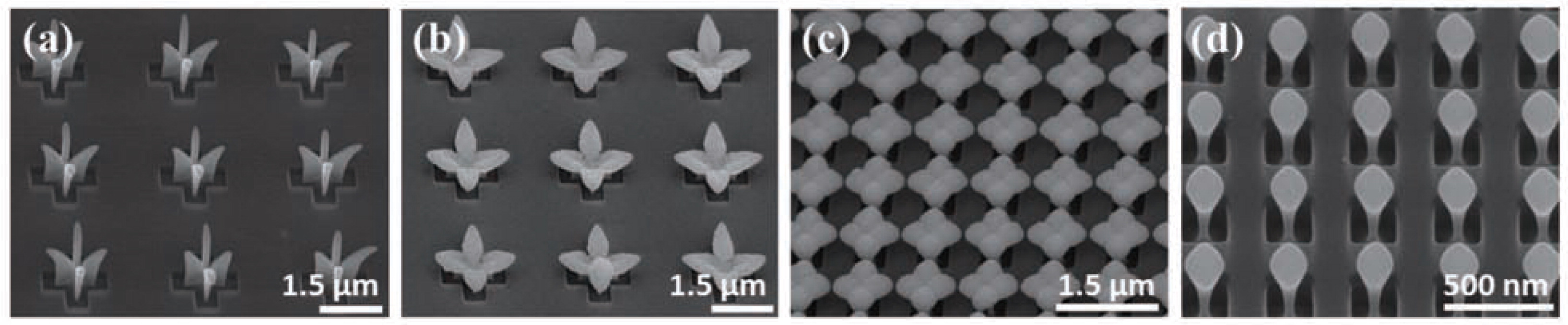
(a)–(d) A variety of shapes of three-dimensional structures consisting of multiple 3-nm Copper nanoparticles. The combination of the ion-induced focusing and the three-dimensional electrostatic scaffold effects realizes selective formation of three-dimensional structures of nanoparticles on the photoresist patterns. (a)–(c) are reprinted with permission from ref 93. Copyright 2011 American Chemical Society.
IAAL possesses potential to be widely applied to a variety of nanodevices, judging from its advantages that it can be applied to any kinds of particles if they are prepared in the form of charged aerosols, and to both conducting and nonconducting substrates without surface modification. In addition, IAAL can produce arrays of multidimensional, multiscale, and multimaterial structures with a simple parallel atmospheric process.
Using IAAL, You et al.89) fabricated a gas sensing device which took advantage of the characteristics of ZnO nanoparticles that their electrical conductivity varied according to the concentration of surrounding gases. Fig. 8(a) shows a SEM image of the lines of 20-nm ZnO nanoparticles deposited on a 200-nm-thick SiO2 film supported on a p-type silicon substrate by using an epoxy mask having 50-μm-wide line openings in the IAAL process. The gas-sensing sensitivity of this sensor was evaluated by examining its response to CO and H2 and, as shown in Fig. 8(b), it exhibits high sensitivity even to the low CO concentration of 1-ppm. Kim et al.92) also demonstrated a gas sensing device by patterning lines of shell-shaped carbon nanoparticles (SCNP) with IAAL.
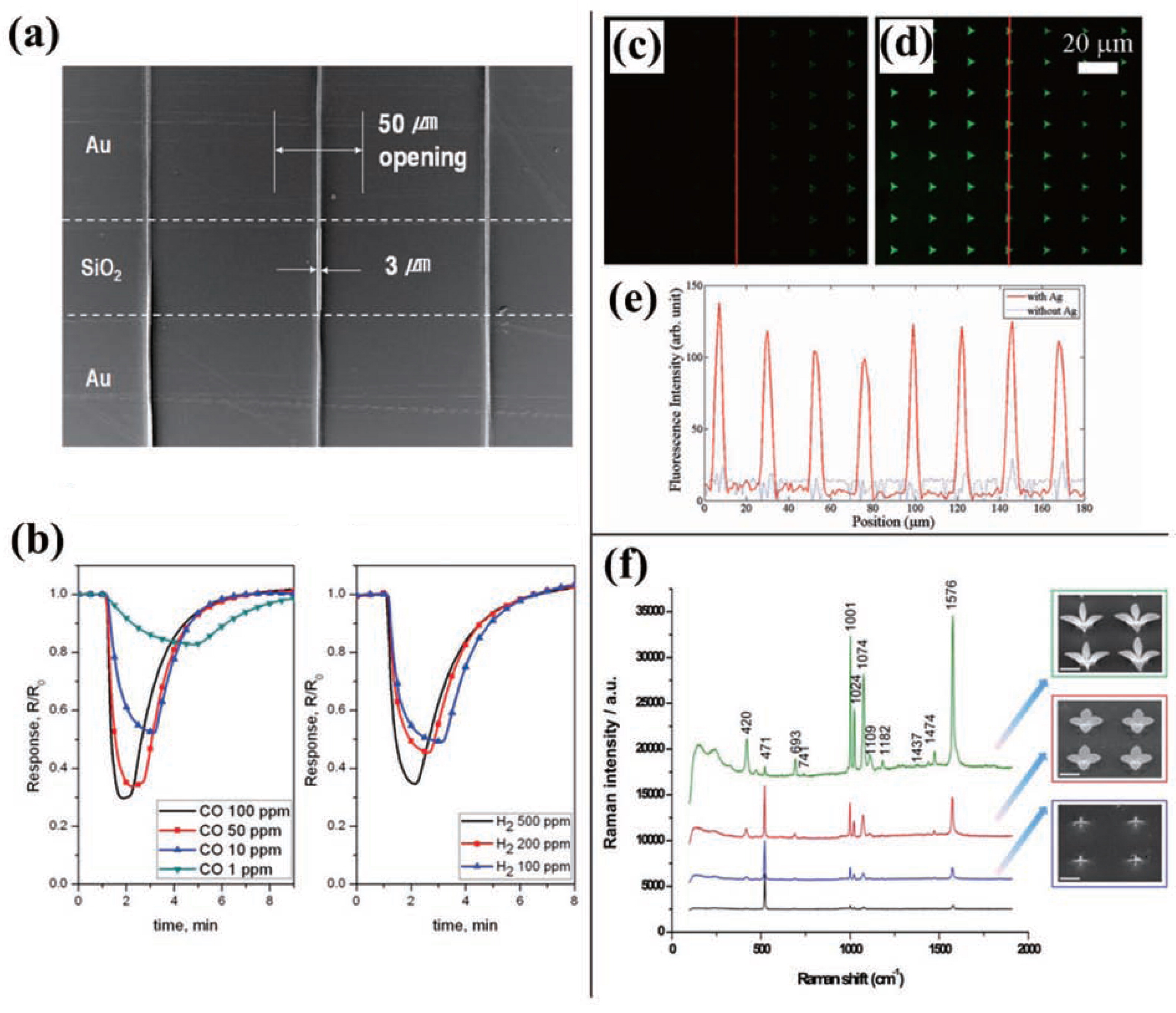
(a)–(b) A gas sensor demonstrated by depositing patterns of ZnO nanoparticles on a silicon substrate coated by 200-nm-thick SiO2 layer. (a) A SEM image of patterns of 3-μm-wide lines composed of 20-nm ZnO particles between two gold electrodes. (b) Sensor responses to CO and H2 gases, respectively. (a) and (b) are reprinted with permission from ref 89. Copyright 2010 Willey-VCH. (c)–(d) Fluorescence images of IgG-FITC (c) without silver particles and (d) with silver particles. (e) A profile of signal intensity observed following the red lines in (c) and (d). (c)–(e) are reprinted with permission from ref 89. Copyright 2010 Willey-VCH. (f) Raman spectra of thiophenol on three-dimensional structures of composite nanoparticles at different growth stages. Samples are composed of copper nanoparticles for the inner part and silver nanoparticles for the outer part. Reprinted with permission from ref 93. Copyright 2011 American Chemical Society.
In addition, Metal enhanced fluorescence (MEF) was effectively observed by depositing silver nanoparticles into the triangular openings of SiO2 followed by the selective deposition of fluorescence-tagged protein nanoparticles with IAAL on top of the silver nanoparticle patterns. From this process, one could avoid wasting proteins on the unwanted nonspecific adsorption88). Fig. 8(c)–(e) show the fluorescence images of IgG-FITC(fluorescein isothiocyanate) (c) without silver particles and (d) with silver particles. Here, the present design of human IgG-FITCs on top of sliver nanoparticles exhibits much strong fluorescent signals compared to the non-silver case.
Surface enhanced Raman scattering (SERS) device provided by IAAL was also demonstrated93). SERS substrates fabricated based on three-dimensional nanoparticle structures by utilizing IAAL showed much increased signals compared to two-dimensional cases. Three SERS substrates were prepared by depositing three-dimensional structures of copper nanoparticles for different deposition times, followed by deposition of silver nanoparticles on them since thiophenol did not chemically bind to copper nanoparticles but to silver. Fig. 8(f) shows the SEM images of the three SERS substrates and the corresponding Raman spectra of thiophenol on those samples. The Raman spectra clearly indicate that the Raman intensity of the full grown three-dimensional structures was noticeably stronger than the case of non-nanoparticles and the intensity increased as the two-dimensional structures grew to three-dimensional structures.
Development of technologies for highly precise assembling or patterning of nanoparticles over large areas is a prerequisite to realize nanodevices which are presently developed to take advantage of the unique properties of nanoparticles. In response to the demand, many research groups have demonstrated novel methods to manipulate nanoparticles. These methods can be classified according to the governing force which is exploited in manipulating nanoparticles. The three most employed forces are electrostatic, capillary and magnetic forces because they can simultaneously occur in a large area and make it possible to design a parallel process. Among them, electrostatic force, the mostly adopted force to manipulate nanoparticles, has brought out a variety of novel methods such as nanoxerography, electrodynamic focusing, biased p-n junction method, and so on. The methods utilizing capillary phenomenon such as micromolding in capillary, template-assisted assembly and dip-pen nanolithography have also presented well-defined arrays of nanoparticles. In addition, there have been some efforts to manipulate nonmagnetic nanoparticles utilizing magnetic force as well as magnetic nanoparticles. Among those patterning methods, IAAL is one of the effective electrodynamic focusing methods, which employs the ion induced focusing concept and, consequently, produces arrays of highly focused assembly made of nanoparticles in three dimensions. The resolution of the deposited assembly using IAAL is controllable with the following parameters: the surface charge density on the patterned mask, the applied voltage on the substrate, the aspect ratio of the photoresist patterns, and the particle charges. IAAL can be applicable to any kinds of nanoparticles prepared in the form of charged aerosols and does not need any surface modifications of a substrate by means of a nanoparticle patterning mask. It is also applicable to nonconducting substrates as well as conducting substrates. Moreover, three-dimensional assembly of nanoparticles can be easily fabricated with IAAL.
This work was supported by the Global Frontier Center for Multiscale Energy Systems funded by National Research Foundation under the Ministry of Education, Science and Technology (2011-0031561). Financial support from BK21 program and WCU (World Class University) multiscale mechanical design program (R31-2008-000-10083-0) through the Korea Research Foundation is gratefully acknowledged. Authors are also affiliated with the Institute of Advanced Machinery and Design, Seoul National University, Seoul 151-742, Republic of Korea.
Hyangki Sung
;%0A%09%09%09newWindow.document.open();%0A%09%09%09newWindow.document.write('<img src=%22./Graphics/30_2013008_9.jpg%22>');%0A%09%09%09newWindow.document.close();%0A%09%09)
Hyangki Sung received her B.S. degree in Mechanical Engineering from Pohang University of Science and Technology (POSTECH), Korea, in 2010. She is currently working toward her Ph.D. degree in Mechanical and Aerospace Engineering at Seoul National University. Her research interests include assembly of nanoparticles, organic light emitting diodes and organic photovoltaics.
Mansoo Choi
;%0A%09%09%09newWindow.document.open();%0A%09%09%09newWindow.document.write('<img src=%22./Graphics/30_2013008_10.jpg%22>');%0A%09%09%09newWindow.document.close();%0A%09%09)
Mansoo Choi received his B.S. (1980) and M.S. (1982) from Seoul National University and Ph.D. (1987) from University of California, Berkeley. After Ph.D., he moved to Chicago to work as an assistant mechanical engineer at Argonne National Laboratory from 1988 to 1991. In 1991, he returned home country, Korea to join in ME department of Seoul National University as an assistant professor and he is now a Professor of School of Mechanical and Aerospace Engineering. He was a Director of National CRI Center for Nano Particle Control from 1997 to 2011. Last year, he became a Director of Global Frontier Center for Multiscale Energy Systems that the Ministry of Education, Science and Technology is going to support up to 2020. As a societal service, he has been working as Co-Editor-in-Chief of the Journal of Aerosol Science from 2004. He served as a Chair for Thermal Engineering Division of KSME in 2009. His current research interests include aerosol synthesis and assembly of nanoparticles and nanodevices.