Special Issue : Frontier in Nanoscale Three-Dimensional Analysis
Three-Dimensional Analysis using Focused Ion Beam and Electron Microscope
2018 Volume 61 Issue 12 Pages 772-777
Details
2018 Volume 61 Issue 12 Pages 772-777
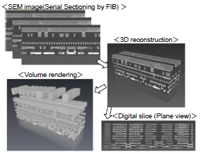
Recently, latest semiconductor devices have three-dimensional (3D) structure and nanostructured materials have 3D distribution of its components. Therefore, 3D analysis methods are required. In this report, some cases that were analyzed using serial sectioning method and TEM tomography method are introduced.