Vacuum and Surface Science
Online ISSN : 2433-5843
Print ISSN : 2433-5835
Volume 61, Issue 12
Special Issue : Frontier in Nanoscale Three-Dimensional Analysis
Displaying 1-15 of 15 articles from this issue
Preface
Special Issue : Frontier in Nanoscale Three-Dimensional Analysis
  • Hiroki TANAKA
    Article type: Overview
    2018 Volume 61 Issue 12 Pages 760-765
    Published: December 10, 2018
    Released on J-STAGE: December 10, 2018
    JOURNAL FREE ACCESS

    Semiconductor devices with complicated structures have been developed, and it is becoming increasingly important to understand three-dimensional (3D) structures of devices with nanometer resolution. The key to successful nanometer-scale 3D analysis is sample preparation technology and it has been highly developed. By combining or correlating multiple physical analyses, limitations of single analysis method are well covered and new information of 3D devices is obtained. Simultaneously acquired multi-signal STEM images are effective for internal structure analysis of 3D devices.

    Editor's pick

    Download PDF (3791K)
  • ―Operation and Device Microstructure―
    Masashi ARITA, Atsushi TSURUMAKI-FUKUCHI, Yasuo TAKAHASHI
    Article type: Current Topics
    2018 Volume 61 Issue 12 Pages 766-771
    Published: December 10, 2018
    Released on J-STAGE: December 10, 2018
    JOURNAL FREE ACCESS

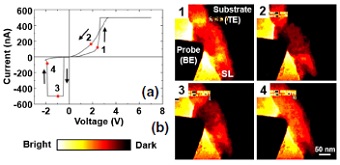
    In-situ transmission electron microscopy (in-situ TEM) has been applied to understand the operation mechanism of resistive random access memories (ReRAMs) and their device degradation and failure. Formation and erasure of the conductive filament (CF) was experimentally confirmed to contribute the ReRAM operation. Very tiny CF was formed at the resistance change, and it grew much with subsequent current flow. Realistic device structure was also investigated.

    Download PDF (3077K)
  • Jun KATO
    Article type: Current Topics
    2018 Volume 61 Issue 12 Pages 772-777
    Published: December 10, 2018
    Released on J-STAGE: December 10, 2018
    JOURNAL FREE ACCESS

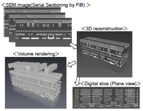
    Recently, latest semiconductor devices have three-dimensional (3D) structure and nanostructured materials have 3D distribution of its components. Therefore, 3D analysis methods are required. In this report, some cases that were analyzed using serial sectioning method and TEM tomography method are introduced.

    Download PDF (4300K)
  • Tadakatsu OHKUBO
    Article type: Current Topics
    2018 Volume 61 Issue 12 Pages 778-783
    Published: December 10, 2018
    Released on J-STAGE: December 10, 2018
    JOURNAL FREE ACCESS

    Microstructures of materials and devices greatly influence the mechanical, electrical, magnetic, and other properties. In order to improve such properties, it is very important to understand the relationship between the microstructure and the properties. Atom probe tomography is a technique which can identify the position of individual atoms and can display the results as 3D tomography. Also, the atomic species are identified based on the time-of-flight measurement. Therefore, all the elements from hydrogen can be analyzed. Although there are several theoretical limitations of this method, the application area is spreading by complementing with other methods such as SEM, TEM and so on. In this paper, the principle and the limitations of the laser assisted atom probe tomography, efforts to improve performance, influence of measuring conditions such as laser wavelength and intensity, and examples of typical application are shown.

    Download PDF (3119K)
  • Shinya HOSOKAWA, Kouichi HAYASHI, Koji KIMURA, Naohisa HAPPO, Tomohiro ...
    Article type: Current Topics
    2018 Volume 61 Issue 12 Pages 784-789
    Published: December 10, 2018
    Released on J-STAGE: December 10, 2018
    JOURNAL FREE ACCESS

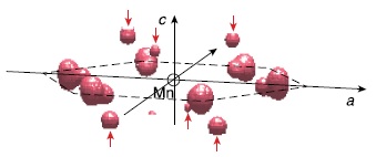
    In recent years, X-ray fluorescence holography (XFH) investigations are remarkably developed to draw three-dimensional (3D) atomic images and to clarify local structures of functional materials, which can compensate for disadvantages of other methods for structural characterizations such as diffraction and X-ray absorption fine structure (XAFS). One of the important topics on the XFH experiments is to find an impurity site in a crystal. The second is to utilize a two-dimensional detector for saving data acquisition time and for conducting valence-selective XFH experiments. In this article, recent progresses of the XFH technique and their applications to functional materials are introduced.

    Download PDF (2784K)
  • Kosuke SUZUKI, Hiroshi SAKURAI
    Article type: Current Topics
    2018 Volume 61 Issue 12 Pages 790-796
    Published: December 10, 2018
    Released on J-STAGE: December 10, 2018
    JOURNAL FREE ACCESS

    Compton scattering is one of the most promising probes which allow us for non-destructive measurement to the practical devices because it uses high-energy X-rays with a high penetration power. By using high-energy X-rays, the Compton scattering enables us to directly measure the light-elements like Li atom. Moreover, a Compton profile, so-called Compton scattered X-ray energy spectrum, directly links to wavefunction of the electrons. In this paper, we demonstrate unique quantitation method of Li ion distribution in a Li ion battery, and temperature distribution in a combustion flame. Our technique opens a novel analyzing pathway for developing the advanced practical devices.

    Download PDF (2304K)
Regular article
  • Ryo ISHIKAWA, Akio NAKANO, Ryunosuke SHIMA, Maki SHIMIZU, Yoshikazu HO ...
    Article type: Regular article
    2018 Volume 61 Issue 12 Pages 797-801
    Published: December 10, 2018
    Released on J-STAGE: December 10, 2018
    JOURNAL FREE ACCESS

    Single-walled carbon nanotubes (CNTs) are light and highly tensile, which makes them a candidate material for space elevator. However, CNTs are not resistant to oxidant. We studied the damage of CNTs caused by exposure to ozone using several kinds of single-walled CNTs with varying crystallinity and morphology. We found a correlation between the initial crystallinity and resistance to ozone : high-crystallinity CNTs with a small number of defects were lightly damaged by ozone exposure, while highly-defective CNTs were further damaged. The thickness of bundling also affected the resistance to ozone. High-crystallinity CNTs forming a thick bundle were most resistant to ozone.

    Download PDF (1576K)
Planning Series
Surface Science and Vacuum Technology
Report
Conference Reports
Science Café
Research Abroad
News & Trends
feedback
Top