e-Journal of Surface Science and Nanotechnology
Online ISSN : 1348-0391
ISSN-L : 1348-0391
Volume 16
Displaying 51-87 of 87 articles from this issue
Conference -ISSS-8-
  • Yasushi Maeda, Kohei Tada, Shin-ichi Yamazaki
    Article type: Conference -ISSS-8-
    Subject area: Environmental and Energy Technology
    2018 Volume 16 Pages 253-256
    Published: June 09, 2018
    Released on J-STAGE: June 09, 2018
    JOURNAL FREE ACCESS
    Supplementary material

    Rhodium porphyrin complexes deposited on carbon support exhibit high activity for electrochemical CO oxidation. As such, they are good candidates for CO-tolerant catalysts in polymer electrolyte fuel cells. For the practical use of rhodium porphyrin complexes, however, their stability in water is of paramount importance. In this study, rhodium (III) octaethylporphyrin chloride was deposited on a highly oriented pyrolytic graphite substrate and observed by atomic force microscopy before and after water treatment. Although treatment with water changed the surface structure of RhOEP/HOPG, the face-on RhOEP layer remained intact. [DOI: 10.1380/ejssnt.2018.253]

    Download PDF (645K)
  • Masaharu Oshima, Daisuke Mori, Aki Takigawa, Akihiko Otsuki, Naoka Nag ...
    Article type: Conference -ISSS-8-
    Subject area: Micro- and Nano-Fabrication
    2018 Volume 16 Pages 257-261
    Published: June 09, 2018
    Released on J-STAGE: June 09, 2018
    JOURNAL FREE ACCESS

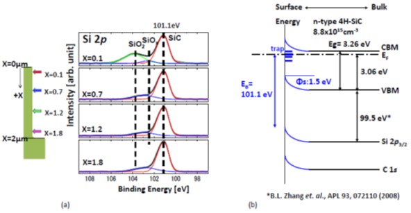
    SiC trench structures having a width of 0.6 μm and a depth of 2.0 μm are fabricated by reactive ion etching (RIE) using a gas mixture of SF6, Ar, and O2. Further, SiC trench structures are cleaved to expose the sidewall for the channel region of a trench MOSFET. These structures were analyzed by pin-point photoelectron spectroscopy using a 100 nm soft-X-ray beam. It is observed that around 2 nm-thick homogeneous carbon-rich layer containing 1—2% F forms on the SiC sidewalls. This may be caused due to the re-deposition of RIE reaction products, CF4 and SiF4, under appropriate conditions to fabricate the trench walls that are approximately vertical using RIE. Further, a carbon-rich layer having a thickness of about 2.4 nm is also formed on the bottom of the SiC trench, suggesting the possibility of selective etching of Si from the SiC substrates. The position of the dominant peak that is associated with the SiC component remains constant regardless of the trench depth, suggesting homogeneous band bending due to the RIE defects, which may explain the reason for no variation being observed in the gate oxide/SiC interface trap density values. Further, the band bending of 1.50 eV that is observed on the sidewall can be attributed to a positively charged carbon vacancy (VC+). [DOI: 10.1380/ejssnt.2018.257]

    Download PDF (1338K)
  • Kohei Tada, Hiroaki Koga, Mitsutaka Okumura, Akihide Hayashi, Yoshinor ...
    Article type: Conference -ISSS-8-
    Subject area: Catalysis
    2018 Volume 16 Pages 267-273
    Published: June 14, 2018
    Released on J-STAGE: June 14, 2018
    JOURNAL FREE ACCESS
    Supplementary material

    In this study, the effect of Cl-adsorption on the reduced rutile TiO2(110) surface during Au atom diffusion on the surface is investigated using density-functional theory-based calculations. This is done in order to investigate the reason for which the co-existence of Cl during Au/TiO2 catalyst preparation enhances the Au cluster aggregation. The calculation results show that the diffusion barrier along the [110] direction is decreased by the Cl adsorption. Hence, the diffusion rate increases when the surface adsorbs Cl. The enhancement of the Au atom diffusion by Cl is one reason for which Cl-elimination is necessary for preparing Au/TiO2 catalysts with high catalytic activity. [DOI: 10.1380/ejssnt.2018.267]

    Download PDF (718K)
  • Naoyuki Matsumoto, Sachiko Ishizawa, Kenji Hata, Don N. Futaba
    Article type: Conference -ISSS-8-
    Subject area: Nano-Materials
    2018 Volume 16 Pages 279-282
    Published: June 16, 2018
    Released on J-STAGE: June 16, 2018
    JOURNAL FREE ACCESS

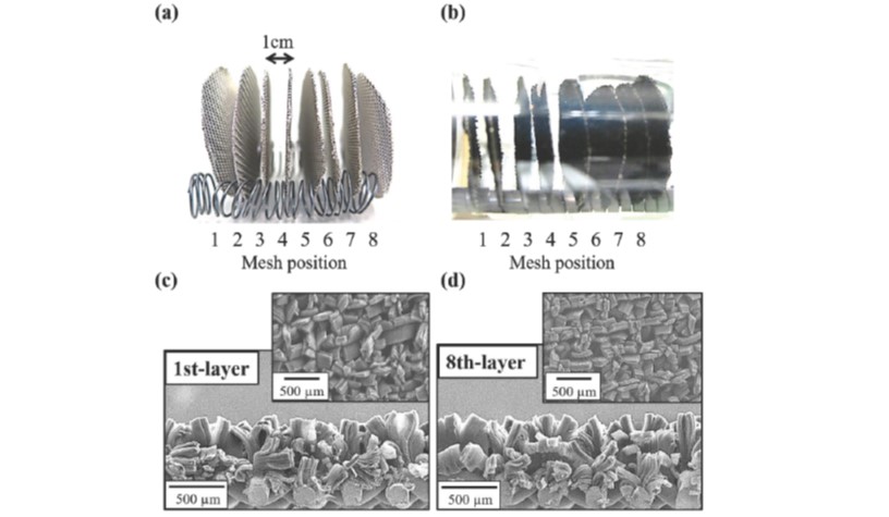
    We demonstrate the high yield synthesis of single-walled carbon nanotubes (SWCNTs) using a multi-layer, three-dimensional (3-D) metal mesh porous substrate consisting of eight parallel and evenly spaced mesh substrates. SWCNT yield in this synthesis improved 78-times compared to that of a single flat nonporous substrate. In addition, the total SWCNT yield was greater than eight-fold (mesh layered number). This yield improvement caused from the two reasons. First, mesh substrate could play a role as higher surface substrates than that of a flat nonporous substrate. Second, it also could achieve gas heating elements to allow the uniform delivery of heated source gases. In addition, CNTs grown were sustained the single-walled structure from the first layer to the final (8th) layer. This architecture leads to achieve the total carbon conversion efficiency of above 80% with single-walled structure (average: 1.2 number of walls). We can demonstrate this process as an interesting alternative approach for the efficient synthesis of high yield SWCNT synthesis for mass production through simply a change to the layered porous substrates (metal meshes). [DOI: 10.1380/ejssnt.2018.279]

    Download PDF (410K)
  • Saule Zholdayakova, Ryota Gemma, Haru-Hisa Uchida, Masashi Sato, Yoshi ...
    Article type: Conference -ISSS-8-
    Subject area: Environmental and Energy Technology
    2018 Volume 16 Pages 298-301
    Published: June 21, 2018
    Released on J-STAGE: June 21, 2018
    JOURNAL FREE ACCESS

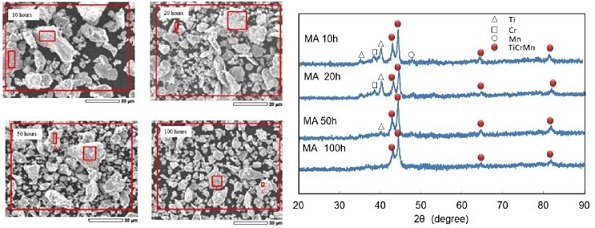
    Hydrogen absorbing alloys have attracted great attention because they are a safe and efficient media for transporting hydrogen energy. AB, AB2, AB5, and A2B-type hydrogen storage compounds and related substituted multi-component alloys have been proposed. In general, titanium-based alloys are among the most promising materials for hydrogen storage. Among the various available types of metal hydrides, AB2 type Ti-Cr-based alloys are the most promising candidates. In particular, there have been many methods for improving the hydrogen sorption properties. One of them is to prepare hydrogen absorbing alloys by mechanical alloying (MA). MA also enables synthesizing various non-equilibrium alloys and has been widely applied to modify properties of hydrogen storage alloys. Thus, MA is possibly the best way for mechanical composition control and mass production of various hydrogen storage alloys. [DOI: 10.1380/ejssnt.2018.298]

    Download PDF (250K)
  • Yongil Kim, Eiichi Nishikawa, Yasuyuki Watanabe
    Article type: Conference -ISSS-8-
    Subject area: Thin Films
    2018 Volume 16 Pages 302-305
    Published: June 21, 2018
    Released on J-STAGE: June 21, 2018
    JOURNAL FREE ACCESS

    Electrospray deposition (ESD) is a method of producing a variety of thin films, and is widely employed for industrial-use electrostatic coatings, such as automotive paint. In ESD, the electrospray phenomenon is utilized to produce nanothin films using a simple device configuration. In this study, we fabricated carbon nanotube (CNT) thin films via ESD, using a multi-walled nanotube solution. We found that irregularities formed on the thin film surface because the surfactant crystallized. However, the CNT thin film, for which sodium dodecyl sulfate (SDS) was not used, exhibited a uniform thickness. [DOI: 10.1380/ejssnt.2018.302]

    Download PDF (908K)
  • Ken Wada, Tetsuroh Shirasawa, Izumi Mochizuki, Masanori Fujinami, Masa ...
    Article type: Conference -ISSS-8-
    Subject area: Instrumentations and Techniques
    2018 Volume 16 Pages 313-319
    Published: June 30, 2018
    Released on J-STAGE: June 30, 2018
    JOURNAL FREE ACCESS

    An experimental system has been developed for the study of low-energy positron diffraction (LEPD) with a slow-positron beam generated by a linear-electron-accelerator (linac). Diffraction patterns of a Ge(001)-2 × 1 surface structure have been observed with a normal positron incidence. This is the first LEPD observation with a linac-based high-intensity pulsed slow-positron beam. [DOI: 10.1380/ejssnt.2018.313]

    Download PDF (600K)
  • Kota Takaoka, Kei Mitsuhara, Masaru Takizawa, Shiro Entani, Seiji Saka ...
    Article type: Conference -ISSS-8-
    Subject area: Thin Films
    2018 Volume 16 Pages 320-323
    Published: July 05, 2018
    Released on J-STAGE: July 05, 2018
    JOURNAL FREE ACCESS

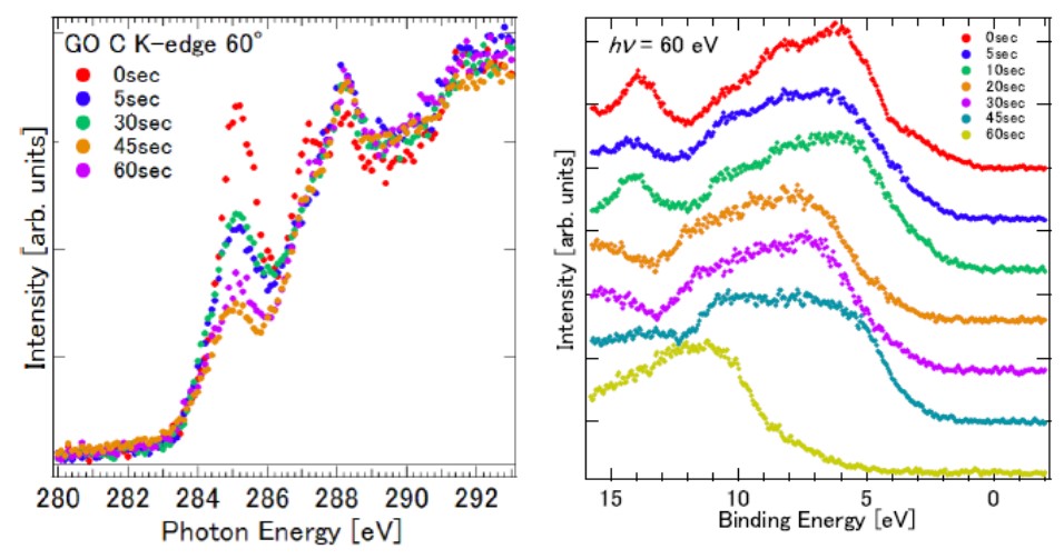
    In order to investigate the process of oxidizing graphene, the chemical and electronic states have been studied by X-ray absorption fine structure (XAFS) and photoelectron spectroscopy (PES) measurements. Single layer graphene oxide was formed on α-Al2O3(0001). After oxidation until 30 s, XAFS results showed a decrease of C π* intensity and an appearance of O π* intensity and PES results showed a similar electronic state. However, 45 s oxidation leaded to a different electronic state, and the O π* intensity decreased for 60 s oxidation. The oxidation is thought to firstly introduce the oxygen functional groups, then to modify the graphene. [DOI: 10.1380/ejssnt.2018.320]

    Download PDF (1099K)
  • Akinori Honda, Hiroshi Itoh
    Article type: Conference -ISSS-8-
    Subject area: Instrumentations and Techniques
    2018 Volume 16 Pages 339-342
    Published: July 21, 2018
    Released on J-STAGE: July 21, 2018
    JOURNAL FREE ACCESS

    Frequency separation between topography and potential scans in Kelvin probe force microscopy (KPFM) was investigated. Topographic images were scanned via the first resonance frequency of the cantilever excited mechanically. Potential images were scanned via the first, second, or third resonance frequency of the cantilever excited electrostatically. Good separation of the mechanical modulation to the cantilever in AC mode and the potential modulation to the probe tip was obtained when the second or third modulation frequency was used. Higher resonance modes led to a decreased capacitive effect between the cantilever and sample, which resulted in better lateral resolution of potential measurements, mainly owing to the tip—sample capacitive effect. The shorter time scale of amplitude change in the cantilever oscillation for the higher resonance frequencies led to well-converged potential measurements. The second and third resonance frequencies are useful for separating signals in KPFM, resulting in better lateral resolution and potential difference measurements of the sample surface. [DOI: 10.1380/ejssnt.2018.339]

    Download PDF (563K)
  • Yongil Kim, Eiichi Nishikawa, Yasuyuki Watanabe
    Article type: Conference -ISSS-8-
    Subject area: Nano-Materials
    2018 Volume 16 Pages 343-346
    Published: July 28, 2018
    Released on J-STAGE: July 28, 2018
    JOURNAL FREE ACCESS

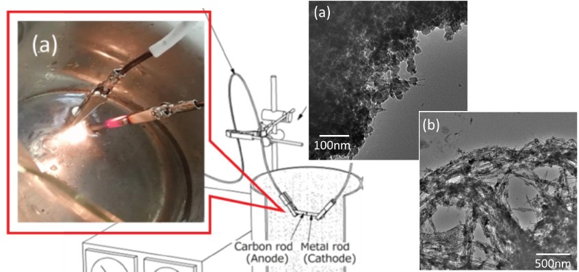
    Carbon nanotubes (CNTs) are produced by an arc discharge method, using carbon for both electrodes along with a metal catalyst for the cathode. In this study, we conducted experiments using four kinds of metals (iron, copper, manganin, and nickel) for the cathode and investigated the difference in product and production yield due to the differences in the metals. The greatest quantity of high quality CNTs was produced with nickel as the metal catalyst, with some CNTs as large as 10 microns. Iron produced almost no CNTs, copper produced linear CNTs, and manganin produced a small quantity of very short CNTs. [DOI: 10.1380/ejssnt.2018.343]

    Download PDF (1185K)
  • Masaki Maekawa, Seiji Sakai, Atsumi Miyashita, Atsuo Kawasuso
    Article type: Conference -ISSS-8-
    Subject area: Instrumentations and Techniques
    2018 Volume 16 Pages 347-350
    Published: July 28, 2018
    Released on J-STAGE: July 28, 2018
    JOURNAL FREE ACCESS

    Nitrogen-implanted p-type GaN films have been investigated through the Doppler broadening of annihilation radiation (DBAR) measurements with spin-polarized positrons and magnetization (MH) measurements. The DBAR spectra showed asymmetry upon magnetic-field reversal at 300 K, while no asymmetry appeared at 30 K. This result indicates that excess electron spins at Ga vacancies are aligned under the application of magnetic field at 300 K, but such spin ordering vanishes at low temperatures. No hysteresis was found in MH curves both at 10 K and 300 K. This means that no macroscopic magnetism appears even though excess electron spins at Ga vacancies are introduced. [DOI: 10.1380/ejssnt.2018.347]

    Download PDF (253K)
  • Naofumi Nishida, Koji Betsumiya, Makoto Sakurai, Takahiro Sakurai, Tos ...
    Article type: Conference -ISSS-8-
    Subject area: Vacuum
    2018 Volume 16 Pages 356-359
    Published: August 02, 2018
    Released on J-STAGE: August 02, 2018
    JOURNAL FREE ACCESS

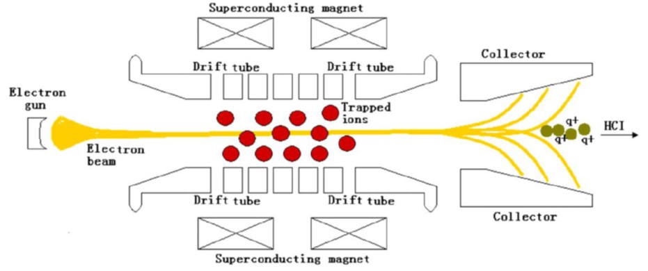
    Electron spin resonance (ESR) measurements were performed on highly oriented pyrolytic graphite (HOPG) samples irradiated with highly charged ions (HCIs). The interaction between a HCI and surfaces results in emission of photons in the range of visible to X-ray, hundreds of secondary electrons, sputtering of secondary ions and modification of surface structure in nanometer scale. In the present experiments, HCIs were produced by electron beam ion source (EBIS) and Ar8+ and Ar14+ were used for the irradiation. ESR measurement provides information on unpaired electrons of the sample. We investigated the dependence of defect formation on charge state and fluence of incident HCIs using ESR. The L1 line appeared in HOPG samples irradiated with HCIs at the low temperature region, and the intensity became larger at higher charge state and higher fluence. [DOI: 10.1380/ejssnt.2018.356]

    Download PDF (355K)
  • Naoya Yamaguchi, Fumiyuki Ishii
    Article type: Conference -ISSS-8-
    Subject area: Electronic Properties
    2018 Volume 16 Pages 360-363
    Published: August 04, 2018
    Released on J-STAGE: August 04, 2018
    JOURNAL FREE ACCESS

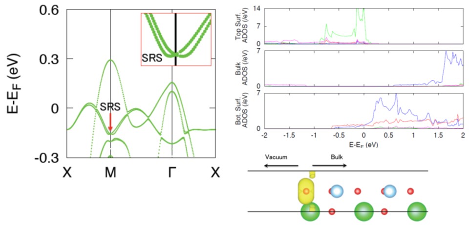
    We investigated the Rashba spin splittings in a compressive-strained SrTiO3(001) ultra thin-film using first-principles calculations. The effect of the polarization due to the compressive strain leads to the 2DEG with large Rashba spin splittings, where the sheet carrier density is of the same order of magnitude as that of the heterostructure LaAlO3/SrTiO3 (∼1014 cm−2). Some localized surface states (SSs) show the giant Rashba coefficient αR larger than 100 meVÅ. [DOI: 10.1380/ejssnt.2018.360]

    Download PDF (361K)
  • Haiya Yang, Takayuki Miyamae, Masato Miyashita
    Article type: Conference -ISSS-8-
    Subject area: Devices and Sensors
    2018 Volume 16 Pages 364-369
    Published: August 09, 2018
    Released on J-STAGE: August 09, 2018
    JOURNAL FREE ACCESS

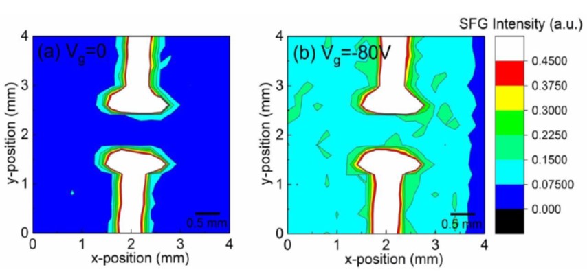
    Charges accumulated at the semiconductor/insulator interface of a top-contact bottom-gate organic field-effect transistors (OFET) with a channel length/width of 1000 μm/1000 μm while applying a negative gate voltage are visualized in a probe region of 4 mm × 4 mm by electric-field induced sum-frequency generation spectroscopy. It is found the charges are accumulated not only inside but also outside the channel of the OFET. The accumulated charges are also found to be uniformly distributed on the semiconductor/insulator interface. The resolution of this mapping technique is explored to be 0.34 mm in the horizontal direction and 0.32 mm in the vertical. [DOI: 10.1380/ejssnt.2018.364]

    Download PDF (488K)
  • Masahiro Yano, Yuki Uozumi, Satoshi Yasuda, Hidehito Asaoka, Chie Tsuk ...
    Article type: Conference -ISSS-8-
    Subject area: Reaction and Dynamics
    2018 Volume 16 Pages 370-374
    Published: August 11, 2018
    Released on J-STAGE: August 11, 2018
    JOURNAL FREE ACCESS

    Real-time scanning tunneling microscope (STM) measurements are performed during the thermal decomposition of an oxide layer on Si(110). Voids in which only oxide is removed are formed during the real-time measurements, unlike the thermal decomposition in which bulk Si is desorbed with oxide. Analysis of the STM images reveals that the measurement induces the decomposition of the oxide layer resulting from electron injection into the defect sites. The activation energy of thermal decomposition decreases by 0.4 eV in the range of 700—780°C. [DOI: 10.1380/ejssnt.2018.370]

    Download PDF (1032K)
  • Ryosuke Umezawa, Makoto Katsura, Satoru Nakashima
    Article type: Conference -ISSS-8-
    Subject area: Nano-Materials
    2018 Volume 16 Pages 376-381
    Published: August 30, 2018
    Released on J-STAGE: August 30, 2018
    JOURNAL FREE ACCESS

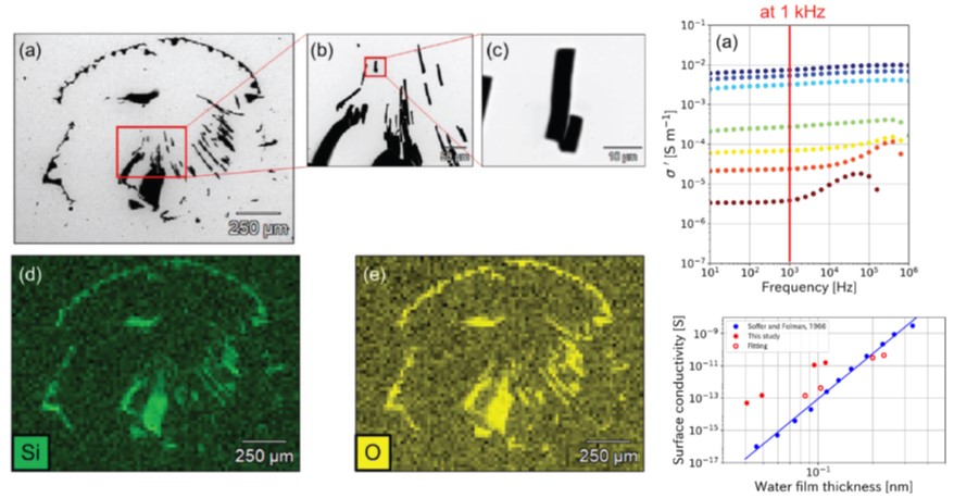
    Electrical conductivity of silica nanoparticles deposited on electrodes from colloidal suspension were measured under controlled relative humidity (RH). The electrical conductivity values at 1 kHz increased with increasing RH. Amounts of water adsorbed on silica nanoparticles were measured by quartz crystal microbalance (QCM) and they also increased with increasing RH. An empirical power law relation was observed between the reported surface conductivity and RH data for a silica glass. By applying this relation to the silica nanoparticles, the water film thicknesses are estimated to be from 0.08 nm to 0.23 nm. The corresponding specific surface area (SSA) becomes smaller (102 m2g1) than the reported value (215 m2g−1), indicating aggregation of the nanoparticles. In fact, aggregated rod-like structures were observed under electron and laser scanning microscopy. The electrical conduction of deposited silica nanoparticles under various RH can be understood by surface conduction in thin water films adsorbed on the nanoparticles. [DOI: 10.1380/ejssnt.2018.376]

    Download PDF (627K)
  • Yongil Kim, Eiichi Nishikawa, Yasuyuki Watanabe
    Article type: Conference -ISSS-8-
    Subject area: Nano-Materials
    2018 Volume 16 Pages 382-386
    Published: September 01, 2018
    Released on J-STAGE: September 01, 2018
    JOURNAL FREE ACCESS

    For the production of carbon nanotubes (CNTs), the underwater arc-discharge method, in comparison to the vacuum arc-discharge method, has some drawbacks, including weak discharge intensity, low discharge sustainability, and low production volumes of CNTs. Likewise, despite its advantages, there are also some disadvantages to the use of arc discharges in foams, as these require additional distillation processes to eliminate foam after CNT production. This study, therefore, investigates an alternative method, replacing conventional foams used as discharge environments with foam made from the surfactant sodium dodecyl sulfate (SDS). Our results indicate that by using an arc discharge in a 0.03% SDS solution, we succeeded in producing aggregated CNTs, and the synthesized CNTs had high linearity and crystallinity. Furthermore, dispersion of the CNTs produced by arc discharge in the surfactant foam was facilitated by ultrasonic processing. [DOI: 10.1380/ejssnt.2018.382]

    Download PDF (483K)
  • Yoshimu Iwanami, Teruo Suzuki, Kazuo Tagawa, Satoshi Yasuno
    Article type: Conference -ISSS-8-
    Subject area: Thin Films
    2018 Volume 16 Pages 396-399
    Published: October 04, 2018
    Released on J-STAGE: October 04, 2018
    JOURNAL FREE ACCESS

    The fuel-saving performance of automotive lubricants greatly depends on the composition and structure of the reaction films that form on metal surfaces through chemical reactions between the additives in the lubricant and the metals. In this study, we prepared reaction films on metal surfaces using two lubricants formulated with different base oils of different degrees of polarity and an anti-wear additive commonly used in automotive engine oils, and examined the chemical state of the films using HAXPES. It was observed that polyphosphates found in the reaction film formed with the lubricant formulated with the polar base oil had shorter chains than those in the reaction film formed with the lubricant formulated with the non-polar base oil. In the latter reaction film, polyphosphates with longer chains may concentrate near the film surface. By contrast, in the former reaction film the polyphosphates may have chains of mostly the same length. [DOI: 10.1380/ejssnt.2018.396]

    Download PDF (731K)
  • Yuki Nakaya, Katsuya Okada, Yudai Ikuno, Satoru Nakashima
    Article type: Conference -ISSS-8-
    Subject area: Reaction and Dynamics
    2018 Volume 16 Pages 411-418
    Published: October 06, 2018
    Released on J-STAGE: October 06, 2018
    JOURNAL FREE ACCESS

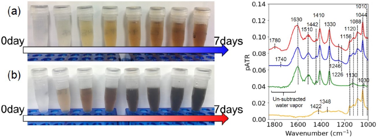
    Progress of the simulated Maillard reaction for 0.1 mol L−1glycine and ribose mixture solution at 80°C for 0—7 days forming humic-like substances in the presence/absence of goethite was examined by ultraviolet-visible (UV-VIS) spectroscopy. 254 nm and 420 nm absorption intensities for the product solutions with goethite increased faster than for those without goethite, indicating enhancement of the reaction progress in the presence of goethite in several days at 80°C. Adsorption onto goethite of reactants of the reaction were directly monitored by attenuated total reflection infrared (ATR-IR) spectroscopy with thin layers of goethite on the ATR crystal (ZnSe). IR spectral changes with time for the reactant solution (0.1 mol L−1 glycine and ribose mixture solution) on the goethite layer suggested fast adsorption within a few hours at room temperature of oxygenated components of glycine onto positively charged goethite surface. In situ heating ATR-IR kinetic measurements of humic-goethite interfaces will be useful for examining mechanisms of surface processes leading to reaction enhancement. [DOI: 10.1380/ejssnt.2018.411]

    Download PDF (1093K)
  • Hikaru Sawahata, Naoya Yamaguchi, Hiroki Kotaka, Fumiyuki Ishii
    Article type: Conference -ISSS-8-
    Subject area: Thin Films
    2018 Volume 16 Pages 427-430
    Published: November 24, 2018
    Released on J-STAGE: November 24, 2018
    JOURNAL FREE ACCESS

    We investigate the effect of the electric field on the edge states in one-bilayer Bi(111) by first-principles calculations. We calculate the band structures of armchair and zigzag Bi nanoribbons. With increasing strength of the electric field E > 2.1 V/Å, the armchair nanoribbon shows a topological phase transition from non-trivial metallic edge states to insulating edge states. However, under the same conditions, the zigzag nanoribbon shows a topological phase transition from non-trivial metallic edge states to trivial metallic edge states. We expect that these findings will contribute to the development of, e.g., spin current switches for use in next-generation devices. [DOI: 10.1380/ejssnt.2018.427]

    Download PDF (3452K)
  • Naonari Sakamoto, Tsunenobu Onodera, Hidetoshi Oikawa, Takuma Dezawa, ...
    Article type: Conference -ISSS-8-
    Subject area: Nano-Materials
    2018 Volume 16 Pages 436-439
    Published: December 22, 2018
    Released on J-STAGE: December 22, 2018
    JOURNAL FREE ACCESS
    Supplementary material

    We have successfully fabricated well-defined Au-core and polydiacetylene-shell hybridized nanoparticles (NPs) having the suitable thickness of dielectric SiO2 layer between Au-core and polydiacetylene-shell by coprecipitation/microwave irradiation method, and subsequent solid-state polymerization process. The resulting hybridized NPs exhibited the significant enhancement of fluorescence intensity, increase in fluorescence quantum yield, and decrease in fluorescence lifetime, compared with polydiacetylene nanocrystals, due to the “emission enhancement” by localized surface plasmon resonance effect, and then would be one of the promising plasmonic nanomaterials toward optical device applications such as intense and stable point light sources. [DOI: 10.1380/ejssnt.2018.436]

    Download PDF (264K)
Conference -ALC '17-
  • Yahachi Saito, Tsuneo Yasue
    Article type: Conference -ALC '17-
    Subject area: Preface
    2018 Volume 16 Pages A1-A2
    Published: October 27, 2018
    Released on J-STAGE: October 27, 2018
    JOURNAL FREE ACCESS

    The 11th International Symposium “Atomic Level Characterization for New Materials and Devices (ALC '17)” under the auspices of the 141st Committee on Microbeam Analysis of the Japan Society for the Promotion of Science (JSPS) was held in Aqua Kauai Beach Resort, Kauai, Hawaii, gathering 251 participants from 19 countries. In this symposium, 209 papers in total, including one Tutorial and three Plenaries, have been presented. Fourteen papers out of them are collected in this special issue. [DOI: 10.1380/ejssnt.2018.A1]

    Download PDF (47K)
  • Masaru Irita, Hitoshi Nakahara, Yahachi Saito
    Article type: Conference -ALC '17-
    Subject area: Nano-Science and -Technology
    2018 Volume 16 Pages 84-87
    Published: April 14, 2018
    Released on J-STAGE: April 14, 2018
    JOURNAL FREE ACCESS

    Generally, nano-resolution X-ray imaging has been achieved using synchrotron radiation facility. The spatial resolution (below 100 nm) achieved with a Fresnel zone plate for focusing the X-ray in SPring-8 lately. We have developed a compact composite of field emission-scanning electron microscope (FE-SEM) with a single isolated multi-walled carbon nanotube (CNT) electron source in our previous study. The spatial resolution of SEM image was estimated as ≃ 10 nm. This result indicates that the electron source we developed is suitable for a point-like X-ray source. We developed two kinds of X-ray microscope; projection-type X-ray microscope (PXM) and transmission-type X-ray microscope (TXM) in this study. The X-ray microscope based on the CNT-FE-SEM was constructed with a metal target for the X-ray source. Developing our X-ray microscope has been miniaturized to a compact size so that it can be placed on a desk. Moreover, the spatial resolution of 400 nm achieved the theoretical resolution limit. Because there is resolution limit by the acceleration voltage of 17 kV for the focused electron beam spot, the spatial resolution is an order of the electron penetration depth. The present study shows a potential that the CNT-based X-ray microscope would be applied to various field studies including the scene of an archaeological site excavation and future planet search. [DOI: 10.1380/ejssnt.2018.84]

    Download PDF (664K)
  • Minfang Zhang, Mei Yang, Toshiya Okazaki, Masako Yudasaka
    Article type: Conference -ALC '17-
    Subject area: Nano-Science and -Technology
    2018 Volume 16 Pages 93-96
    Published: April 20, 2018
    Released on J-STAGE: April 20, 2018
    JOURNAL FREE ACCESS

    Quantification of the cellular uptake of nanomaterials is crucial for studies of their toxicity and medical applications. However, our knowledge of the behaviors of carbon nanotubes (CNTs) in cells or tissues remains incomplete due to the lack of appropriate methods for quantitative analysis. Here, we present a unique methodology for quantitatively assessing the cellular uptake of CNTs, taking advantage of their absorption of light in the near-infrared region. Measurement of CNT concentration in cell lysates by monitoring absorbance at 750 nm enabled highly accurate quantification of CNTs accumulated within cells. In a comparative study of eight commercially available CNTs with size ranging from 30 nm to 400 nm, we obtained the first quantitative evidence that cellular uptake of CNTs by RAW264.7 macrophages depends on the sizes, specifically on the widths of their bundles in dispersion, regardless of type or manufacturer. [DOI: 10.1380/ejssnt.2018.93]

    Download PDF (646K)
  • Rie Shishido, Masuo Itoh, Masahito Uchikoshi, Shigeru Suzuki
    Article type: Conference -ALC '17-
    Subject area: Interdisciplinary
    2018 Volume 16 Pages 150-155
    Published: May 16, 2018
    Released on J-STAGE: May 16, 2018
    JOURNAL FREE ACCESS

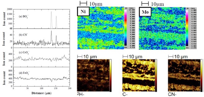
    This paper overviews analytical results of the microscopic distribution of minor elements in iron-based alloys, obtained by secondary ion mass spectrometry (SIMS). Since trace amounts of some elements play crucial roles in the properties of steels, it is very important to analyze their distribution in the microstructure of iron-based alloys. Time of flight SIMS (TOF-SIMS) and conventional dynamic SIMS are powerful methods for detecting minor elements in iron-based alloys and analyzing their distribution in the microstructure of these materials. In this paper, we report several examples of the microscopic distribution of minor elements in iron-based alloys, which provide significant information on complicated phenomena related to the alloy microstructure. The depth profiles obtained by dynamic SIMS showed how a specific trace element penetrates the alloy matrix, indicating that the diffusion of the element is strictly related to the microstructure. On the other hand, high-sensitivity and high-spatial-resolution TOF-SIMS was used to characterize the microscopic distribution of trace elements, such as boron and nitrogen, in iron-based alloys, which is also related to the alloy microstructure. [DOI: 10.1380/ejssnt.2018.150]

    Download PDF (408K)
  • Takashi Hattori, Masatomo Hattori, Masakuni Ozawa
    Article type: Conference -ALC '17-
    Subject area: Nano-Materials
    2018 Volume 16 Pages 172-176
    Published: May 19, 2018
    Released on J-STAGE: May 19, 2018
    JOURNAL FREE ACCESS

    The CeO2 NP layer on Al2O3(0001) prepared by dipping method using CeO2 NPs colloid solution showed less contacted state among the primary particles even after heat treatment at 1000°C in air. The surface reduction behavior of CeO2 NP layer on Al2O3(0001) was investigated by XPS under the Ar+ sputtering in vacuum. The result indicates that Ar+ sputtering induced a considerable reduction of CeO2 NP layer on Al2O3(0001) and its final ratio of Ce3+ was 79%. In comparison with CeO2 powder, the difference between their final ratio of Ce3+ (79% and 68%) was small. Therefore, it was indicated that the Ar+ sputtering induced the reduction of Ce4+ to Ce3+ in CeO2 by mainly physical effect, however the chemical effect in low oxygen pressure could be attributed to the local thermal energy transfer induced by kinetic energy of Ar+ ions. The substrate-stabilized and dispersed CeO2 NPs showed slightly accelerated capacity in reducing behavior of CeO2. [DOI: 10.1380/ejssnt.2018.172]

    Download PDF (364K)
  • Claus M. Schneider
    Article type: Conference -ALC '17-
    Subject area: Electronic Properties
    2018 Volume 16 Pages 177-185
    Published: May 25, 2018
    Released on J-STAGE: May 25, 2018
    JOURNAL FREE ACCESS

    The electron spin governs many phenomena in modern condensed matter physics, such as magnetism, superconductivity, etc. Often, minute details in the electronic structure determine the physical behavior of a material. Photoelectron emission—being the most established approach to explore electronic structures—is currently entering a new era thanks to a breathtaking development in light sources, spectrometer concepts, and spin detectors. In particular, the evolution in novel highly efficient electron spin polarimeters opens up new experimental opportunities and permits unequaled insights into the electronic structure. This contribution will discuss several examples in this field of spin-dependent interactions and spin-based phenomena. A prominent one refers to the class of topological insulators, where strong spin-orbit coupling (SOC) causes a unique spin-momentum locking around the Dirac cone. Transition metal dichalcogenides consist of quasi-2D layers coupled by v. d. Waals interactions. Here, strong SOC leads to pronounced hybridization effects. We also address fundamental issues in ferromagnetism, e.g., the complex interplay of SOC and exchange interaction, causing characteristic k-, spin- and symmetry-dependent band mixing. Using spin- and time-resolved photoemission we explore ultrafast spin dynamics in ferromagnets driven by strong ultrashort laser pulses. We find the changes in both majority and minority spin states to take place on a 100 fs time scale and to be compatible with band mirroring.
    In this contribution, we will discuss several new aspects of spin-dependent and spin-resolved photoemission covering both static and dynamic issues of electronic states. [DOI: 10.1380/ejssnt.2018.177]

    Editor's pick

    Download PDF (5053K)
  • Takumi Hamaoka, Ayako Hashimoto, Kazutaka Mitsuishi, Masaki Takeguchi
    Article type: Conference -ALC '17-
    Subject area: Instrumentations and Techniques
    2018 Volume 16 Pages 247-252
    Published: June 09, 2018
    Released on J-STAGE: June 09, 2018
    JOURNAL FREE ACCESS

    We propose an experimental depth-sectioned imaging method based on annular dark-field scanning confocal electron microscopy (ADF-SCEM). Four-dimensional (4D) datasets, consisting of 2D probe images taken at every probe position during 2D raster scanning, were acquired with an aberration-corrected scanning transmission electron microscope. A series of depth-sectioned images were constructed by processing a single 4D dataset. A pinhole and a stage-scan system used in earlier studies were not required in the present data acquisition. Optimal observation conditions for the 4D data acquisition in the ADF-SCEM mode are outlined from multislice simulations. [DOI: 10.1380/ejssnt.2018.247]

    Download PDF (2425K)
  • Yuma Kato, Muneaki Yamamoto, Akiyo Ozawa, Yu Kawaguchi, Akinobu Miyosh ...
    Article type: Conference -ALC '17-
    Subject area: Structure
    2018 Volume 16 Pages 262-266
    Published: June 14, 2018
    Released on J-STAGE: June 14, 2018
    JOURNAL FREE ACCESS

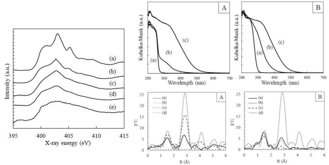
    To promote photocatalytic activity of gallium oxides (Ga2O3) on CO2 reduction with water under visible light irradiation, we have tried nitrogen doping into Ga2O3 with different crystalline structures. In diffuse reflectance UV-vis spectra, absorption bands appeared in the visible light region after the nitrogen doping and the absorption edge shifted to a longer wavelength region with increasing nitrogen doping temperature. N K-edge XANES analysis clearly showed two kinds of nitrogen species doped in the samples; gallium nitride (GaN) species and molecular like nitrogen. In XRD patterns, nitrogen doping at temperatures above 823 K, gallium nitride phases appeared while the original crystal structures of gallium oxide samples maintained when nitrogen doping temperature was less than 823 K. However, photocatalytic CO2 reduction under visible light irradiation was insignificant for all the nitrogen doped samples, because nitrogen doped in Ga2O3 samples was unstable in water under the visible light irradiation. [DOI: 10.1380/ejssnt.2018.262]

    Download PDF (584K)
  • Yuki Ikezoe, Takahide Oya
    Article type: Conference -ALC '17-
    Subject area: Nano-Materials
    2018 Volume 16 Pages 274-278
    Published: June 14, 2018
    Released on J-STAGE: June 14, 2018
    JOURNAL FREE ACCESS

    We propose antennas that use carbon-nanotube-composite papers, i.e., “paper antennas.” We use metal molds to punch press antenna-shaped carbon-nanotube-composite papers in concrete. Carbon-nanotube-composite paper is a composite material that is made by mixing carbon nanotubes with pulp from ordinary paper, and it can be easily fabricated by using a technique that is similar to the techniques for making Japanese washi paper. We prepare 8 × 6 cm2 of rectangle-shaped carbon-nanotube-composite paper containing 200 mg of multi-wall carbon nanotubes and 1000 mg of raw pulp. Then, we obtain our “loop antenna paper” from the composite paper by punch pressing. Our antennas have a four-turned coil with 2-mm wide wire and a 1-mm wide gap between the wires. The measurements of our paper antenna showed 370 mH of inductance and 6.6 μF of capacitance at 100 Hz. In addition, we measured the electromagnetic induction in our paper antennas. We believe that our antennas can be utilized in contactless paper IC cards that will be used in an IoT-based future. [DOI: 10.1380/ejssnt.2018.274]

    Download PDF (478K)
  • Masaru Takizawa, Akihiro Hata, Kei Mitsuhara, Takeshi Tanaka
    Article type: Conference -ALC '17-
    Subject area: Electronic Properties
    2018 Volume 16 Pages 283-285
    Published: June 16, 2018
    Released on J-STAGE: June 16, 2018
    JOURNAL FREE ACCESS

    An ultraviolet-ray aided machining (U-RAM), which attempts to add a chemical reaction through ultraviolet-ray irradiation to a mechanical polishing, is a promising procedure to obtain a flat surface of SiC in a short time. In order to investigate how chemical states change in the U-RAM process, we have performed X-ray absorption fine structure measurements. As a result, it was found that a mixed compound other than SiO2 was produced on the SiC surface by the U-RAM. We think that polishing efficiency of U-RAM is better than ordinary mechanical polishing because of generating the mixed compound of Si—C—O. [DOI: 10.1380/ejssnt.2018.283]

    Download PDF (314K)
  • Ichiro Ohnishi, Toshihiro Suzuki, Kouji Miyatake, Yu Jimbo, Yorinobu I ...
    Article type: Conference -ALC '17-
    Subject area: Nano-Science and -Technology
    2018 Volume 16 Pages 286-288
    Published: June 16, 2018
    Released on J-STAGE: June 16, 2018
    JOURNAL FREE ACCESS

    Sensitivity of energy dispersive X-ray spectroscopy (EDS) in scanning transmission electron microscopy (STEM) has been significantly improved with a recent detection system with large-sized silicon drift detectors (SDDs). The detection solid angle for the latest system, composed of two windowless SDDs, is better than 2 steradians. In combination with a spherical aberration corrector for STEM, the system allows us to observe an atomic resolution elemental map. On the other hand, in situ experiments under various conditions such as heating, cooling, and gas environments have been conducted by using chip-based specimen holders, which are developed owing to fabrication technology of micro electro mechanical systems (MEMS). The aberration corrected microscopy with such a special holder allows us to observe morphological and chemical changes of samples under various conditions at atomic resolution. In this paper, the observation and analysis results of in situ applications is reported by using the aberration corrected microscope with the EDS system and the in situ sample holders. [DOI: 10.1380/ejssnt.2018.286]

    Download PDF (891K)
  • Chuhei Oshima, Masahiko Tomitori, Tatsuya Shimoda, Anto Yasaka, Hirota ...
    Article type: Conference -ALC '17-
    Subject area: Instrumentations and Techniques
    2018 Volume 16 Pages 294-297
    Published: June 21, 2018
    Released on J-STAGE: June 21, 2018
    JOURNAL FREE ACCESS

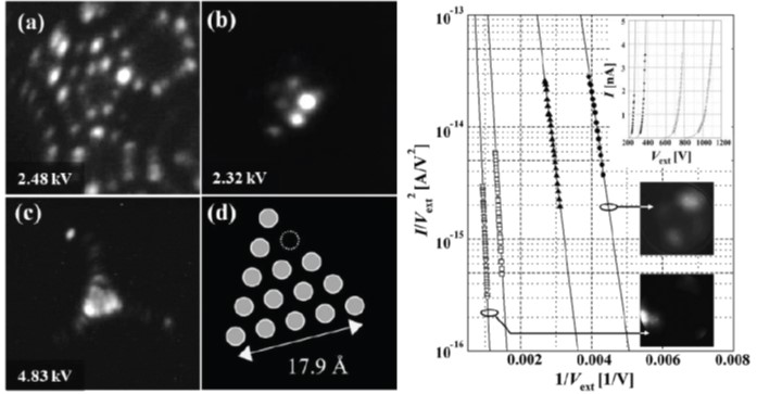
    A single-atom termination (SAT) tip of Ir-W is one of the most promising candidates among various gas-field-ionization ion sources (GFIS) and field emission (FE) tips. In this work, we investigated thermal stability of the SAT tip with increasing the tip temperature. Above 1300 K, the SAT tip was destroyed, which was consistent with the surface phase transition of the monolayer Ir covered W(111) surface [J. J. Kolodziej, T. E. Madey, J. W. Keister, and J. E. Rowe, Phys. Rev. B 65, 075413 (2002)]. The SAT tip is thermodynamically stable only under negative electric bias in the temperature rang below 1300 K. If the SAT tip was broken accidentally, it was repaired for many times only by heating at the negative bias. The demountable character of the SAT tip was also confirmed. [DOI: 10.1380/ejssnt.2018.294]

    Download PDF (161K)
  • Hirotaka Asai, Ryota Kawai, Fumiya Matsubara, Hidekazu Murata, Eiji Ro ...
    Article type: Conference -ALC '17-
    Subject area: Nano-Science and -Technology
    2018 Volume 16 Pages 306-309
    Published: June 21, 2018
    Released on J-STAGE: June 21, 2018
    JOURNAL FREE ACCESS

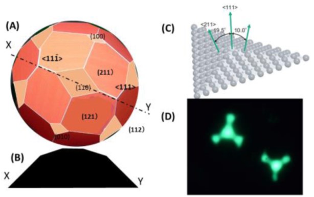
    Tungsten (W) nanopyramids coated with noble metal films can function as highly coherent electron sources. This study aims to grow nanopyramids by employing long-distance surface diffusion of palladium (Pd) atoms. Collodion (also known as nitrocellulose) containing PdO powder was coated on the regions far from the W tip and was used as a source of Pd atoms. Annealing the W tip in UHV resulted in a change in the field ion microscopy (FIM) pattern. The resultant FIM images showed three equivalent {211} planes adjacent to the {111} planes of the W tips. However, with the proposed method, the apex of the W tip was not a single atom, but a wide triangle corresponding to the subsurface of an ideal nanopyramid. [DOI: 10.1380/ejssnt.2018.306]

    Download PDF (221K)
  • Yuto Takagi, So-Hee Kang, Kohei Matsumura, Takeki Azuma, Bunbunoshin T ...
    Article type: Conference -ALC '17-
    Subject area: Nano-Science and -Technology
    2018 Volume 16 Pages 324-328
    Published: July 14, 2018
    Released on J-STAGE: July 14, 2018
    JOURNAL FREE ACCESS

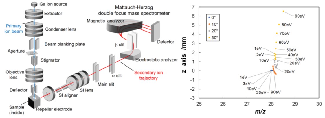
    Secondary ion mass spectrometry can analyze all elements and has high versatility. In our laboratory, we have established a method of sputtering the whole sample from the side by using partial primary beam called Shave-off method, which increases spatial resolution and eliminates an effect originated by surface roughness. Furthermore, designing the ion optics that can enlarge and converge the emitted secondary ions from the cross section of the micro sample on the detector, high-precision three-dimensional distribution data with surface resolution of several nanometer level and depth direction resolution of several tens of nanometer level can be obtained at high speed. However, the secondary ions trajectory and the ion aberration caused by the lens in the Shave-off condition have not been verified. In this study, we have constructed a simulation of calculating the trajectory of emitted ions from the Shave-off cross section. It is expected that the simulation will be of great help and powerful tool for future development. [DOI: 10.1380/ejssnt.2018.324]

    Download PDF (741K)
  • Taisei Ide, Koki Fujiwara, Tatsuya Hashimoto, Kouhei Kanda, Daiki Aiha ...
    Article type: Conference -ALC '17-
    Subject area: Nano-Materials
    2018 Volume 16 Pages 406-410
    Published: October 04, 2018
    Released on J-STAGE: October 04, 2018
    JOURNAL FREE ACCESS

    In this work, Al-doped ZnO nanoparticles encapsulated with amorphous SiO2 were prepared by the wet chemical method. The obtained precursor was annealed and the nanoparticle sizes were controlled by adjusting the annealing temperature. These nanomaterials showed ferromagnetic behavior, even though the ZnO bulk crystal was diamagnetic. The results of electrical conductivity and XANES suggested that ferromagnetism of the Al-doped nanoparticles was results of carrier transport and oxygen vacancies. The Al-doped ZnO nanoparticles are extremely interesting from the perspective of solid state physics. [DOI: 10.1380/ejssnt.2018.406]

    Download PDF (466K)
Errata
feedback
Top